

Page 1
现货库存、技术资料、百科信息、热点资讯,精彩尽在鼎好!
e
Product Description
Sirenza Microdevices’ SPA-2318 is a high efficiency GaAs
Heterojunction Bipolar Transistor (HBT) amplifier housed in a
low-cost surface-mountable plastic package. These HBT
amplifiers are fabricated using molecular beam epitaxial growth
technology which produces reliable and consistent performance
from wafer to wafer and lot to lot.
This product is specifically designed for use as a driver amplifier
for infrastructure equipment in the 1960 and 2140 MHz bands. Its
high linearity makes it an ideal choice for multi-carrier and digital
applications.
The matte tin finish on Sirenza’s lead-free package utilizes a post
annealing process to mitigate tin whisker formation and is RoHS
compliant per EU Directive 2002/95. This package is also manufactured with green molding compounds that contain no antimony
trioxide nor halogenated fire retardants.
VC1
VBIAS
RFIN
VPC2
Active
Bias
RFOUT/
VC2
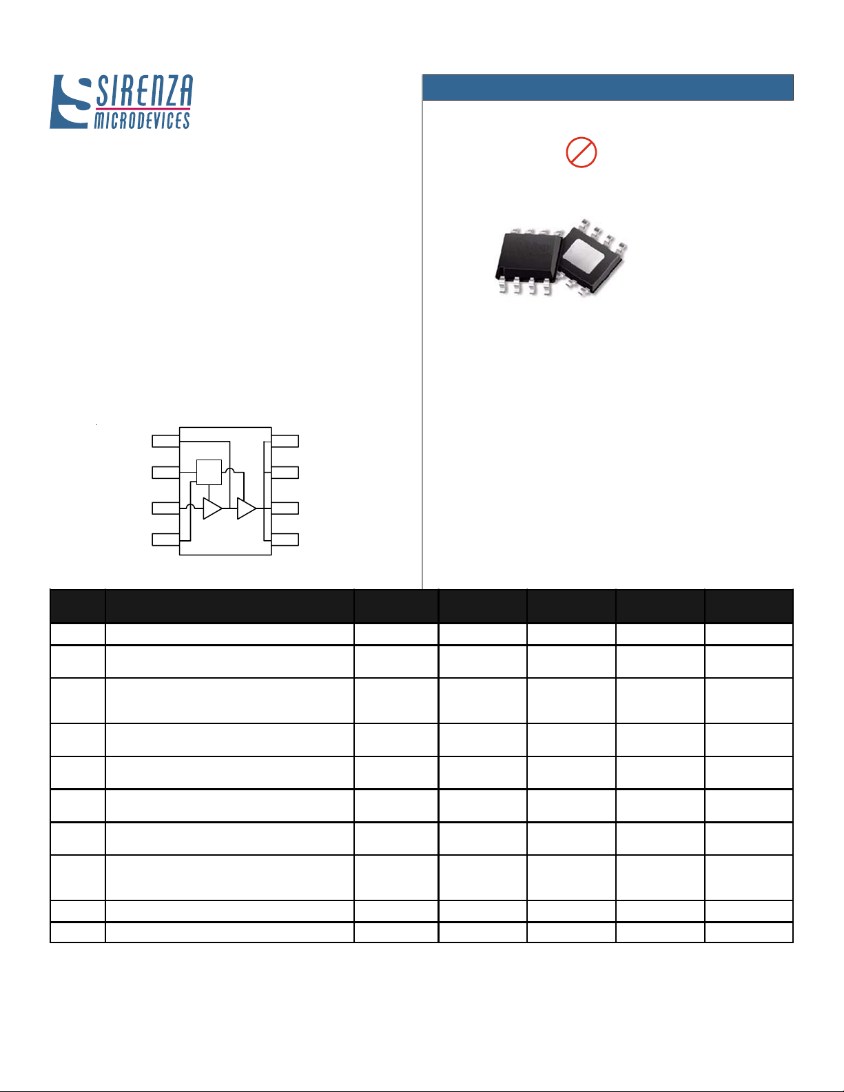
SPA-2318
RoHS Compliant
Pb
Green
SPA-2318Z
1700-2200 MHz 1 Watt Power Amp
with Active Bias
Product Features
• Now available in Lead Free, RoHS
Compliant, & Green Packaging
• High Linearity Performance:
+21 dBm IS-95 Channel Pwr at -55 dBc ACP
+20.7 dBm W-CDMA Channel Pwr at -50dBc ACP
+47 dBm Typ. OIP3
• On-chip Active Bias Control
• High Gain: 24 dB T yp. at 1960 MHz
• Patented High Reliability GaAsHBT T echnology
• Surface-Mountable Plastic Package
Applications
• W-CDMA Systems
• PCS Systems
• Multi-Carrier Applications
& Packag
Preliminary
Symbol
ACP
VSWR Input VSWR
OIP
Para m e ters : Tes t Co n d itions :
= 50 Ohms Temp = 25ºC, Vcc = 5.0V
Z
0
f
Frequency of Operation MHz 1700 2200
0
P
Output Power at 1dB Compression
1dB
A d ja c e nt C hanne l Pow e r
IS- 95 @ P
W-CDMA @ P
S
S m all Sig nal G ai n
21
Outp ut Thi rd O rde r Interc ep t Poi nt
3
Power out per tone = +14dBm
NF Noise Fi g ure
Devic e Current
I
CC
Device Voltage
V
CC
R
Therma l Resistance (junction - lead), TL = 85ºC ºC/W 31
th j-l
= 21.0 dB m
OUT
OUT
[1,2]
[1,2]
[1,2]
[1,2]
[1]
= 20.7 dBm
[1,2]
[1]
[2]
f = 1960 MHz
f = 2140 MHz
f = 1960 MHz
f = 2140 MHz
f = 1960 MHz
f = 2140 MHz
f = 1960 MHz
f = 2140 MHz
f = 1960 MHz
f = 2140 MHz
f = 1960 MHz
f = 2140 MHz
Ib ia s = 10 mA
Ic1 = 70 mA
Ic2 = 320 mA
Units Min. Typ. Max.
dBm
dBc -55.0
dB
-
-
dBm
dB
mA 360 400 425
V
22.5
4.75 5.0 5.25
29.5
29.5
-50.0 -47.0
24.0
23.5 25.0
1.6:1
1.6:1
46.5
47.0
5.5
5.5
[1] Optimal ACP tune [2] Optimal IP3 tune
The information provided herein is believed to be reliable at press time. Sirenza Microdevices assumes no responsibility for inaccuracies or omissions. Sirenza Microdevices assumes no responsibility for the use of this
information, and all such information shall be entirely at the user’s own risk. Prices and specifications are subject to change without notice. No patent rights or licenses to any of the circuits described herein are implied or
granted to any third party. Sirenza Microdevices does not authorize or warrant any Sirenza Microdevices product for use in life-support devices and/or systems. Copyright 2002 Sirenza Microdevices, Inc. All worldwide rights
reserved.
Phone: (800) SMI-MMIC http://www.sirenza.com303 S. Technology Court, Broomfield, CO 80021
1
EDS-101432 Rev H
Page 2
SP A-2318 1700-2200 MHz 1 Watt Power Amp.
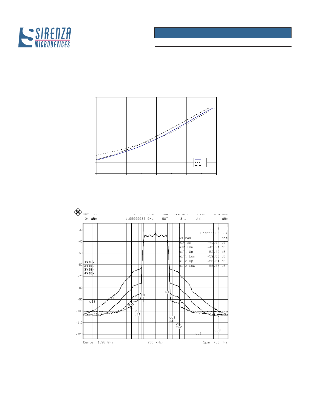
ACP Optimized 1960 MHz Application Circuit Dat a, Icc=400mA, Vcc=5V
IS-95, 9 Channels Forward
1960 MHz Adjacent Channel Power
-40
-45
-50
-55
dBc
-60
-65
-70
-75
16 18 20 22 24
vs. Channel Output Power
dBm
25C
-40C
85C
IS-95 CDMA at 1960 MHz
24 dBm
21 dBm
17 dBm
13 dBm
T=25oC
23.75
Phone: (800) SMI-MMIC http://www.sirenza.com303 S. Technology Court, Broomfield, CO 80021
2
EDS-101432 Rev H
Page 3
SP A-2318 1700-2200 MHz 1 W att Power Amp.
ACP Optimized 1960 MHz Application Circuit Dat a, Icc=400mA, Vcc=5V
31
30
29
28
dBm
27
26
25
1.93 1.94 1.95 1.96 1.97 1.98 1.99
GHz
Input/Output Return Loss,
P1dB vs Frequency
Isolation vs Frequency, T=25
0
-5
-10
-15
-20
dB
-25
-30
-35
-40
1.93 1.94 1.95 1.96 1.97 1.98 1.99
GHz
°°
°C
°°
25C
85C
-40C
S11
S12
S22
30
27
24
dB
21
18
15
1.93 1.94 1.95 1.96 1.97 1.98 1.99
GHz
Device Current vs. Source Voltage
Gain vs. Frequency
600
500
400
300
200
Device Current (mA)
100
0
0123456
25C
-40 C
85C
V
(V)
cc
25C
85C
-40C
Phone: (800) SMI-MMIC http://www.sirenza.com303 S. Technology Court, Broomfield, CO 80021
3
EDS-101432 Rev H
Page 4

1930 - 1990 MHz Schematic
External Connection
SP A-2318 1700-2200 MHz 1 Watt Power Amp.
Vcc
10uF Tantalum
68pF
Ic1
1
2
3
4
1.0pF
1.5pF(IP3)
1.2nH
6.8K
Ibias
°
, 7.3
Ω
Z=63
18nH
2.2pF(ACP)
300 Ohm
1200pF
Vpc
1930 - 1990 MHz Evaluation Board Layout
Vcc
C5
C4
Short
L2
L1
C3
C1
R1
C2
R2
Vpc
C6
C7
L3
C8
Tune for optimal ACP performance
Sirenza Microdevices
ECB-101161 Rev. C
SOIC-8 PA
Eval Board
1000pF
Ic2
8.2pF
8
7
6
5
Z=50 Ω, 13.2°
20 nH
2.2pF
Tune for optimal ACP performance
Ref. D es. Value Part Numbe r
C1
C2 1200pF, 5% Rohm MCH18 series
C3 1.0pF, ±0.25pF Rohm MCH18 series
C4 68pF, 5% Rohm MCH18 series
C5 10uF, 10% AVX TAJB106K020R
C6 1000pF, 5% Rohm MCH18 series
C7 8.2pF, ±0.5pF Rohm MCH18 series
C8 2.2pF, ±0.25pF Rohm MCH18 series
C9
C9 20pF, 5% Rohm MCH18 series
L1 1.2nH, ±0.3nH Toko LL1608-FS series
L2 18nH, 5% Toko LL1 60 8-FS se rie s
L3 20nH, 5% Coilcraft HQ 0805 series
R1 6.8K Ohm, 5% Rohm MCR03 series
R2 300 Ohm, 5% Rohm MCR03 series
20pF
1.5pF, ±0.25pF (IP3)
2.2pF, ±0.25pF (ACP)
Rohm MCH18 s eries
Phone: (800) SMI-MMIC http://www.sirenza.com303 S. Technology Court, Broomfield, CO 80021
4
EDS-101432 Rev H
Page 5

SP A-2318 1700-2200 MHz 1 W att Power Amp.
ACP Optimized 2140 MHz Application Circuit Dat a, Icc=400mA, Vcc=5V
W-CDMA setup is PCCPCH+PSCH+SSCH+CPICH+PICH+64 DPCH,
10.5 dB peak to average @ 0.001% probability
W-CDMA at 2.14 GHz Adjacent Channel Power
vs. Channel Output Power
dBc
-40
-45
-50
-55
-60
-65
-70
16 17 18 19 20 21 22
dBm
W-CDMA at 2.14 GHz
T=25oC
25C
-40C
85C
21.6
Phone: (800) SMI-MMIC http://www.sirenza.com303 S. Technology Court, Broomfield, CO 80021
5
EDS-101432 Rev H
Page 6

SP A-2318 1700-2200 MHz 1 Watt Power Amp.
ACP Optimized 2140 MHz Application Circuit Data, Icc=400mA, Vcc=5V
31
30
29
28
dBm
27
26
25
2.11 2.12 2.13 2.14 2.15 2.16 2.17
25C
85C
-40C
GHz
Input/Output Return Loss,
P1dB vs Frequency
0
Isolation vs Frequency, T=25
-5
-10
-15
-20
dB
-25
-30
-35
-40
2.11 2.12 2.13 2.14 2.15 2.16 2.17
GHz
°°
°C
°°
S11
S12
S22
30
27
24
dB
21
18
15
2.11 2.12 2.13 2.14 2.15 2.16 2.17
GHz
Device Current vs. Source Voltage
Gain vs. Frequency
600
500
400
300
200
Device Current (mA)
100
0
0123456
25C
-40 C
85C
V
(V)
cc
25C
85C
-40C
Phone: (800) SMI-MMIC http://www.sirenza.com303 S. Technology Court, Broomfield, CO 80021
6
EDS-101432 Rev H
Page 7

2110 - 2170 MHz Schematic
SP A-2318 1700-2200 MHz 1 W att Power Amp.
Vcc
10uF Tantalum
External Connection
2.7nH
6.8K Ω
1.5pF (IP3)
2.2pF (ACP)
2110 - 2170 MHz Evaluation Board Layout
C2
Short
L2
L1
C1
Note: All induct ors are
Toko LL1608-FS unless
not ed otherw ise
R1
C7
R2
Z=63 Ω , 21.7°
Ic1
5.6nH
1
2
3
Ibias
4
1800pF
300 Ω
Vpc
C6
Tune for optimal ACP performance
Sirenza Microdevices
ECB-101161 Rev. C
C8
Vpc
SOIC-8 PA
Eval Bo ard
Vcc
C3
C4
C5
L3
56pF
1000pF
5.6pF
8
7
6
5
Z=50 Ω, 11.6°
Tune for optimal ACP performance
0.1uF Tantalum
C9
Ic2
18 nH
39pF
1.8pF
Ref. D es. Value Part N umber
1.5pF, ±0.25pF (IP 3)
C1
2.2pF, ±0.25pF (ACP)
C2 56pF, 5% Rohm MCH18 series
C3 10uF, 10% AVX TAJB106K020R
C4 1000pF, 5% Rohm MCH18 series
C5 5.6pF, ±0.5pF Rohm MCH18 series
C6 1.8pF, ±0.25pF Rohm MCH18 series
C7 1800pF, 5% Rohm MCH18 series
C8 0.1uF, 10% Matsuo 267M3502104K
C9 39pF, 5% Rohm MCH18 series
L1 2.7nH, ±0.3nH Toko LL1608-FS series
L2 5.6nH, ±0.3nH Toko LL1608-FS series
L3 18nH, 5% Toko LL1608-FS serie s
R1 6.8 K Ohm, 5% Ro hm MCR03 series
R2 300 Ohm, 5% Rohm MC R0 3 s erie s
Rohm MCH18 s eries
Phone: (800) SMI-MMIC http://www.sirenza.com303 S. Technology Court, Broomfield, CO 80021
7
EDS-101432 Rev H
Page 8

SP A-2318 1700-2200 MHz 1 Watt Power Amp.
Pin # Function Description
1 VC1 VC 1 is the supply voltage for the first sta ge transistor. The configuration as
shown on application schematic is required for optimum RF performance.
2 Vbias Vbias is the bias control pin for the active bias network. Recommended
configuration is shown in the Application Schematic.
3 RF In RF input pin. This pin requires the use of an external DC blocking capacitor as
shown in the Application Schematic.
4 VPC2 VPC2 is the bias control pin for the active bias network for the second stage.
The recommended co nfiguration is shown in the Appli cati o n Schemati c.
5, 6, 7, 8 RF Out/VC2 RF output and bias pins. Bias should be supplied to this pin through an external
RF choke. Because DC biasing is present on this pi n, a DC blocking capacitor
should be used in most applications (see application schematic). The supply
side of the bias network should be well bypassed. An output matching network is
necessary for optimum performance.
EPAD Gnd Exposed area on the bottom side of the package needs to be soldered to the
ground plane of the board fo r thermal and RF performance. Several vias should
be located under the EPAD as shown in the recommended land pattern (page 9).
Simplified Device Schematic
4
2
ACTIVE BIAS
NETWORK
3
1
2
ACTIVE BIAS
NETWORK
Caution: ESD sensitive
Appropriate precautions in handling, packaging and testing devices must be observed.
The Moisture Sensitivity Level rating for this device is level 1
(MSL-1) based on the JEDEC 22-A113 standard classification.
No special moisture packaging/handling is required during
storage, shipment, or installation of the devices.
5-8
Absolute Maximum Ratings
Parameter (Ta = 25ºC) Absolute
Max. Supply Current (I
Max. Supply Current (I
Max. Device Voltage (V
Max. RF Input Power 16 dBm
Ma x. Junct io n Temp. (T
Max. Storage Temp. +150 ºC
Operation of this device beyond any one of these limits
may cause permanent damage. For reliable continuous
operation, the de vice voltage and current must not exce ed
the maximum operating values specified in the table on
page one.
Bias Conditions should also satisfy the following
expression:
) at V
C1
) at V
C2
) at Icc typ. 6.0 V
CC
) +160 ºC
J
I
(max) < (TJ - TL)/Rth,j-l
CCVCC
typ. 150 mA
CC
typ. 750 mA
CC
Limit
Phone: (800) SMI-MMIC http://www.sirenza.com303 S. Technology Court, Broomfield, CO 80021
8
EDS-101432 Rev H
Page 9

SP A-2318 1700-2200 MHz 1 W att Power Amp.
Package Outline Drawing
(See SMDI MPO-101644 for tolerances, available on our website)
.236 [5.994]
.155 [3.937]
TOP VIEW
.194 [4.928]
SIDE VIEW
876 5
1324
Beveled Edge
.045 [1.143]
.035 [.889]
.016 [.406].050 [1.27]
.061 [1.549]
.008 [.203]
.003 [.076]
SEATING PLANE
BOTTOM VIEW
.058 [1.473]
SEE DETAIL A
.194 [4.93]
.013 [.33] x 45°
.155 [3.937]
END VIEW
EXPOSED PAD
.
0
0
8
PARTING LINE
.025
5°
DETAIL A
Note: DIMENSIONS ARE IN INCHES [MM]
Part Identification Marking
Lot ID
SP A-2318
Lot ID
SP A-2318Z
Part Number Ordering Information
Part Number Reel Size Devices/Reel
SPA-2318 7" 500
SPA-2318Z 7" 500
Recommended Land Pattern
0.150 [3.81]
Plated-Thru Holes
(0.015" Dia, 0.030" Pitch)
Machine
Screws
0.080 [2.03]
0.050 [1. 2 7]
0.140 [3. 5 6]
0.300 [7.62]
0.020 [0.51]
Phone: (800) SMI-MMIC http://www.sirenza.com303 S. Technology Court, Broomfield, CO 80021
9
EDS-101432 Rev H
 Loading...