

Datasheet SP9500AN, SP9500AS, SP9500BN, SP9500BS, SP9500JN Datasheet (Sipex Corporation)
...Page 1

®
SP9500
12–Bit, Voltage Output D/A Converter
■ Low Power – 1.1mW
■ Voltage Output, 0.5V to 4.5V Range
■ Single +5 Volt Supply
■ 1.4 MHz Multiplying Bandwidth
(2-Quadrant)
■ Standard 3-Wire Serial Interface
■ 8–pin (0.15") SOIC and Plastic DIP
Packages
DESCRIPTION…
The SP9500 is a low power 12-Bit Digital-to-Analog Converter. It features 0.5 to 4.5V output
swing when using +5volt supply. The converter uses a standard 3–wire serial interface
compatible with SPI™, QSPI™ and Microwire™. The output settling-time is specified at 7.5µs. The
SP9500 is available in 8–pin 0.15" SOIC and DIP packages, specified over commercial and
industrial temperature ranges.
V
REF
DAC
REGISTER
LATCH
DAC
+
–
V
OUT
AGND
SHIFT
REGISTER
D
SCLKCS
IN
SP9500DS/04 SP9500 12-Bit, Voltage Output D/A Converter © Copyright 2000 Sipex Corporation
1
Page 2
ABSOLUTE MAXIMUM RATINGS
These are stress ratings only and functional operation of the device
at these or any other above those indicated in the operation
sections of the specifications below is not implied. Exposure to
absolute maximum rating conditions for extended periods of time
may affect reliability.
VDD - DGND ..................................................................-0.3V,+6.0V
V
................................................................................DGND, V
REF
AGND .......................................................................... DGND, V
DIN..................................................................................DGND, V
Power Dissipation
Plastic DIP .......................................................................... 375mW
(derate 7mW/°C above +70°C)
Small Outline ...................................................................... 375mW
(derate 7mW/˚C above +70˚C)
DD
REF
DD
SPECIFICATIONS
(Typical at 25˚C; T
PARAMETER MIN. TYP. MAX. UNITS CONDITIONS
DIGITAL INPUTS
Logic Levels
V
IH
V
IL
2 Quad, Input Coding Binary
REFERENCE INPUTS Note 5
V
REF
AGND Voltage Range 0.5 4.5 Volts
Input Resistance 11 13.9 kΩ DIN = 1365; code dependent
ANALOG OUTPUT
Gain
–B, –K ±0.5 ±2.0 LSB Note 3
–A, –J ±1.0 ±4.0 LSB Note 3
Initial Offset Bipolar ±0.25 ±3.0 LSB DIN = 0
Voltage Range 0.5 4.5 Volts
Output Current ±1.0 mA
≤ TA ≤ T
MIN
; VDD = +5V, DGND = 0V, V
MAX
= +3.5V; AGND = +1.5V; CMOS logic level digital inputs; specifications apply to all grades unless otherwise noted.)
REF
2.4 Volts
0.8 Volts
Voltage Range 0.5 4.5 Volts
±1.0 ±5.0 LSB V
= 4.5V; AGND = 0.5V
REF
STATIC PERFORMANCE
Resolution 12 Bits
Integral Linearity
–B, –K ±0.25 ±0.5 LSB Note 3
–A, –J ±0.5 ±1.0 LSB Note 3
Differential Linearity
±0.5 LSB V
= 4.5V; AGND = 0.5V
REF
–B, –K ±0.25 ±0.75 LSB
–A, –J ±0.25 ±1.0 LSB
Monotonicity Guaranteed
DYNAMIC PERFORMANCE
Settling Time
Small Signal 1 µs to 0.012%
Full Scale 7.5 µs to 0.012%, V
Slew Rate 0.6 V/µs
= 0.5 to 4.5V
OUT
Multiplying Bandwidth 1.4 MHz
STABILITY
Gain 15 ppm/˚C t
Scale Zero 15 ppm/˚C t
SP9500DS/04 SP9500 12-Bit, Voltage Output D/A Converter © Copyright 2000 Sipex Corporation
MIN
MIN
to t
to t
MAX
MAX
2
Page 3
SPECIFICATIONS (continued)
(Typical at 25˚C; T
PARAMETER MIN. TYP. MAX. UNITS CONDITIONS
POWER REQUIREMENTS Note 5
V
–J, –K 0.22 0.34 mA
–A, –B 0.22 0.50 mA
Power Dissipation 1.1 mW
SWITCHING
CHARACTERISTICS
CS Setup Time
(t
SCLK Fall to CS Fall
Hold Time
(t
SCLK Fall to CS Rise
Hold Time
(t
SCLK High Width
(tCH)40 ns
SCLK Low Width
(tCL)40 ns
DIN Setup Time
(tDS)50 ns
≤ TA ≤ T
; VDD = +5V, DGND = 0V, V
MIN
MAX
DD
)25 ns
CSS
)20 ns
CSH0
)0 ns
CSH1
= +3.5V; AGND = +1.5V; CMOS logic level digital inputs; specifications apply to all grades unless otherwise noted.)
REF
+5V, ±3%; Note 4, 5
DIN Hold Time
(tDH)0 ns
CS High Pulse Width
(t
)30 ns
CSW
ENVIRONMENTAL AND
MECHANICAL
Operating Temperature
–J, –K 0 +70 °C
–A, –B –40 +85 °C
Storage –60 +150 °C
Package
–_N 8-pin Plastic DIP
–_S 8-pin 0.15" SOIC
Notes:
1. Integral Linearity, for the SP9500, is measured as the arithmetic mean value of the magnitudes of the
greatest positive deviation and the greatest negative deviation from the theoretical value for any given
input condition.
2. Differential Linearity is the deviation of an output step from the theoretical value of 1 LSB for any two
adjacent digital input codes.
3. 1 LSB = (V
4. V
= AGND = 2.5V.
REF
-AGND)/4,096.
REF
5. The following Power up sequence is recommended: VDD (+5V), VREF.
SP9500DS/04 SP9500 12-Bit, Voltage Output D/A Converter © Copyright 2000 Sipex Corporation
3
Page 4
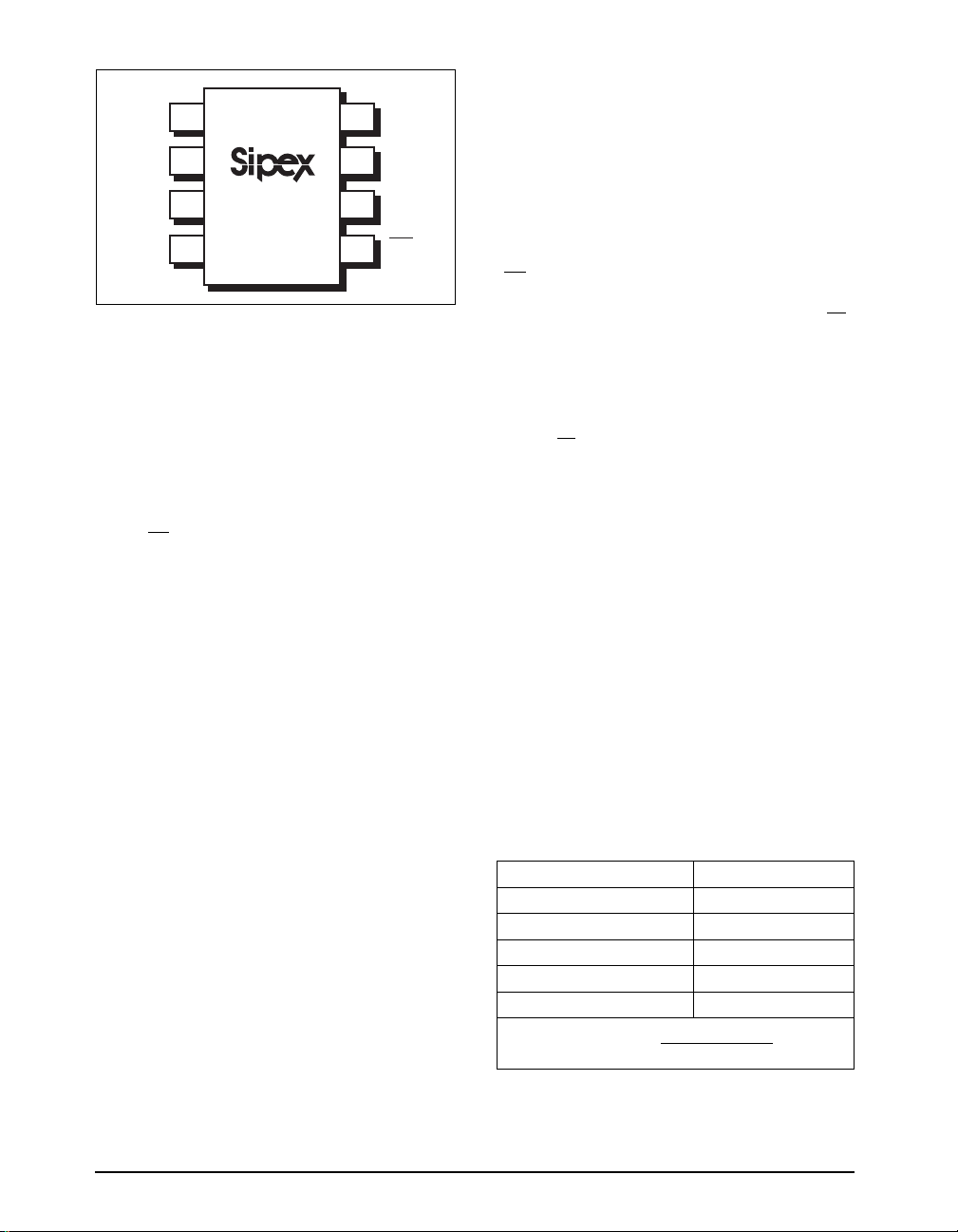
PINOUT – 8-PIN PLASTIC DIP & SOIC
V
OUT
V
DD
1
2
8
7
V
REF
AGND
THEORY OF OPERATION
The SP9500 consists of four main functional
blocks – the input shift register, DAC register,
12-Bit D/A converter and a output buffer
amplifier, Figure 1.
SCLK
D
IN
3
4
SP9500
6
5
DGND
CS
PIN ASSIGNMENTS
Pin 1- V
- Voltage Output.
OUT
Pin 2- VDD - +5V Power Supply Input.
Pin 3- SCLK - Serial Clock Input.
Pin 4- DIN - Serial Data Input.
Pin 5- CS - Chip Select Input.
Pin 6 - DGND - Digital Ground
Pin 7- AGND - Analog Ground.
Pin 8- V
- Reference Input.
REF
FEATURES...
The SP9500 is a low power 12–Bit Digital-toAnalog Converter. The converter features 0.5 to
4.5 volt output swings with a single +5V supply.
The input coding format used is standard binary,
Table 1.
The input shift register is used to convert the
serial input data stream to a parallel 12–Bit
digital word. The input data is shifted on positive clock (SCLK) edges when the Chip Select
(CS) signal is in the “low” state. The MSB is
loaded first and LSB last. No shifting of the
input data occurs when the Chip Select (CS)
signal is in the “high” state.
The DAC register is used to store the digital
word which is sent to the R–2R DAC. Its value
is updated on the positive transition of the Chip
Select (CS) signal.
The 12–Bit D/A converter is an “inverted” R-2R
ladder network. The DAC itself is implemented
with precision thin-film resistors and CMOS
transmission gate switches. The resistor network is laser-trimmed to achieve better than 12–
Bit accuracy. The D/A converter is used to
convert the 12-bit input word to a precision
voltage.
The operational amplifier is a rail-to-rail input,
rail-to-rail output CMOS amplifier. It is capable
of supplying 1mA of load current in the 1.5 to
3.5 output voltage range. The initial offset voltage is laser-trimmed to improve accuracy. Settling time is 7.5 µs for a full scale output transition to 0.012% accuracy.
This Digital-to Analog Converter uses a standard 3–wire interface compatible with SPI™,
QSPI™ and Microwire™. The output settling
time is specified at 7.5 µs to full 12-bit accuracy
when driving a 10KΩ, 10pF load combination.
The SP9500 Digital-to-Analog Converter is
ideally suited for applications such as ATE,
process controllers, robotics and instrumentation. The SP9500 is available in an 8-pin 0.15"
SOIC and 0.3" PDIP packages, specified over
MSB LSB
1111 1111 1111 V
1111 1111 1110 V
0000 0000 0001 AGND + 1 LSB
0000 0000 0000 AGND
Table 1. Binary Coding
INPUT OUTPUT
- 1 LSB
REF
- 2 LSB
REF
(V
-AGND)
1 LSB =
REF
12
2
commercial and industrial temperature ranges.
SP9500DS/04 SP9500 12-Bit, Voltage Output D/A Converter © Copyright 2000 Sipex Corporation
4
Page 5

0 CODE 4095
DNLE, INLE Plots
USING THE SP9500
+0.5 lsb
DNLE
-0.5 lsb
+0.5 lsb
INLE
-0.5 lsb
External Reference
The R-2R DAC input resistance is code dependent and is minimum (11kΩ) at code 1365 and
2731. And, it is nearly infinite at code 0. Because of the code-dependent nature of the reference inputs, a high quality, low output impedance amplifier should be used to drive the V
and AGND inputs.
REF
Serial Clock and Update Rate
The SP9500 maximum serial clock rate (SCLK)
is given by 1/(tCH+tCL) which is approximately
12.5 MHz. The digital word update rate is limited by the chip select period, which is 12 X
DAC
DAC
REGISTER
REGISTER
D
IN
Figure 1. Detailed Block Diagram
SHIFT
REGISTER
121
LATCH
SCLK periods plus the CS high pulse width t
This is equal to a 1 µs or 1 MHz update rate.
However, the DAC settling time to 12–Bits is 7.5
µs, which for full scale output transitions would
limit the update rate to 125 kHz.
Logic Interface
The SP9500 is designed to be compatible with
TTL and CMOS logic levels. However, driving
the digital inputs with TTL level signals will
increase the power consumption of the part by
300 µA. In order to achieve the lowest power
consumption use rail-to-rail CMOS levels to
drive the digital inputs.
V
REF
12
DAC
AGND
+
–
V
OUT
CSW
.
V
OUT
WHERE…
=
V
OUT
=
V
DAC
V
DAC
D
IN
4096
x (V
()
- AGND) + AGND
REF
V
REF
D
IN
+
–
V
AGND
Figure 2. Transfer Function
SP9500DS/04 SP9500 12-Bit, Voltage Output D/A Converter © Copyright 2000 Sipex Corporation
DAC
5
Page 6
CS
SCLK
t
CSHO
t
t
t
CH
t
CSS
t
DH
t
DS
CL
t
CSH1
CSW
DIN
DB11
Figure 3. Timing Diagram
Figure 4. Microwire Connection
DB10
SCLK
SP9500
SCLK
SP9500
DIN
CS
DIN
CS
DB9
N/C
N/C
DB8
SK
SO
I/O
SI
MICROWIRE
SK
MOSI
I/O
MISO
PORT
SPI
PORT
DB0
CPOL = 0, CPHA = 0
Figure 5. SPI Connection
SP9500DS/04 SP9500 12-Bit, Voltage Output D/A Converter © Copyright 2000 Sipex Corporation
6
Page 7
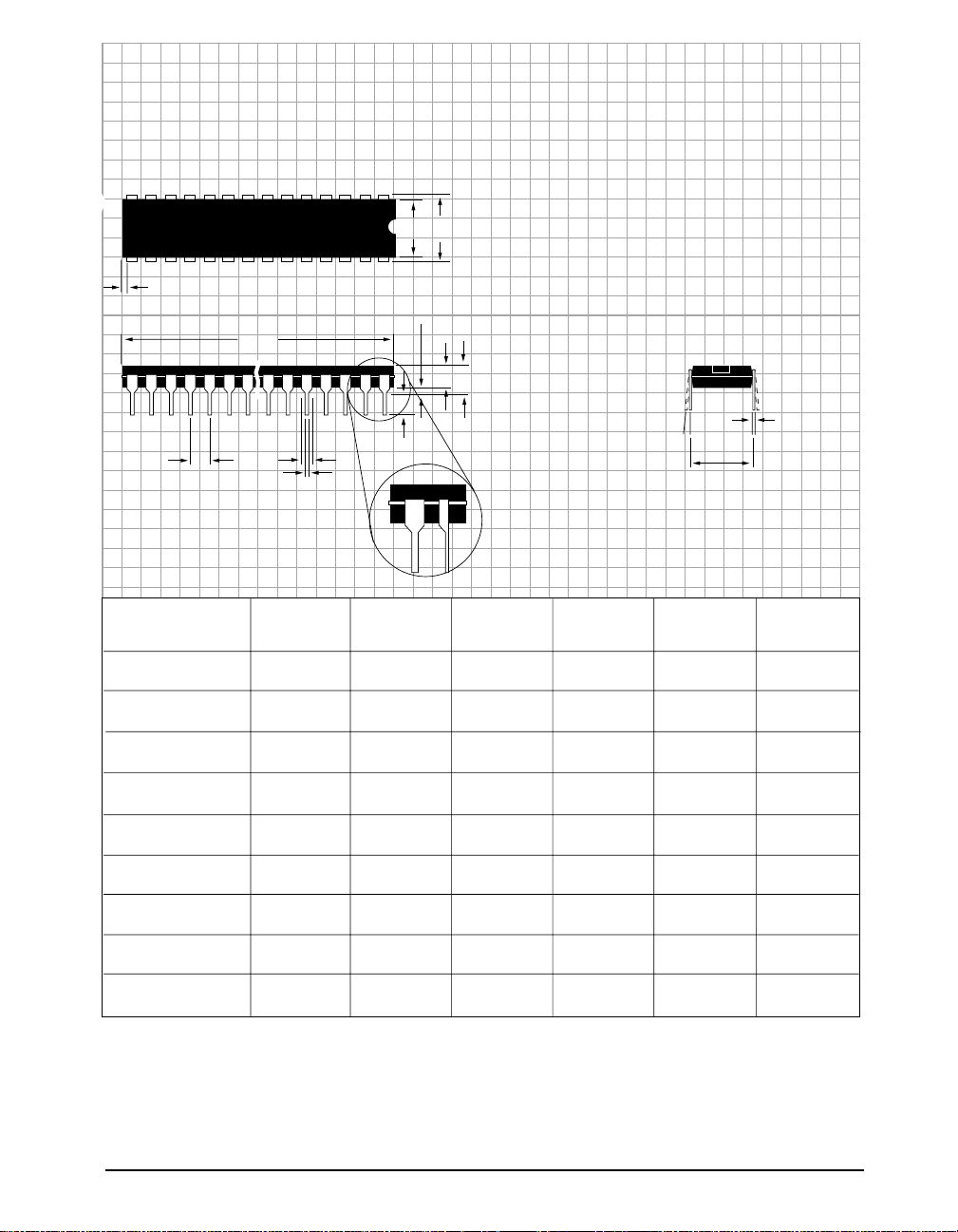
D1 = 0.005" min.
(0.127 min.)
D
e = 0.100 BSC
(2.540 BSC)
B1
B
ALTERNATE
END PINS
(BOTH ENDS)
PACKAGE: PLASTIC
DUAL–IN–LINE
(NARROW)
E1
E
A1 = 0.015" min.
(0.381min.)
A = 0.210" max.
(5.334 max).
A2
L
C
Ø
eA = 0.300 BSC
(7.620 BSC)
DIMENSIONS (Inches)
Minimum/Maximum
(mm)
A2
B
B1
C
D
E
E1
L
Ø
0.115/0.195
(2.921/4.953)
0.014/0.022
(0.356/0.559)
0.045/0.070
(1.143/1.778)
0.008/0.014
(0.203/0.356)
0.355/0.400
(9.017/10.160)
0.300/0.325
(7.620/8.255)
0.240/0.280
(6.096/7.112)
0.115/0.150
(2.921/3.810)
0°/ 15°
(0°/15°)
0.115/0.195
(2.921/4.953)
0.014/0.022
(0.356/0.559)
0.045/0.070
(1.143/1.778)
0.008/0.014
(0.203/0.356)
0.735/0.775
(18.669/19.685)
0.300/0.325
(7.620/8.255)
0.240/0.280
(6.096/7.112)
0.115/0.150
(2.921/3.810)
0°/ 15°
(0°/15°)
0.115/0.195
(2.921/4.953)
0.014/0.022
(0.356/0.559)
0.045/0.070
(1.143/1.778)
0.008/0.014
(0.203/0.356)
0.780/0.800
(19.812/20.320)
0.300/0.325
(7.620/8.255)
0.240/0.280
(6.096/7.112)
0.115/0.150
(2.921/3.810)
0°/ 15°
(0°/15°)
18–PIN
0.115/0.195
(2.921/4.953)
0.014/0.022
(0.356/0.559)
0.045/0.070
(1.143/1.778)
0.008/0.014
(0.203/0.356)
0.880/0.920
(22.352/23.368)
0.300/0.325
(7.620/8.255)
0.240/0.280
(6.096/7.112)
0.115/0.150
(2.921/3.810)
0°/ 15°
(0°/15°)
20–PIN
0.115/0.195
(2.921/4.953)
0.014/0.022
(0.356/0.559)
0.045/0.070
(1.143/1.778)
0.008/0.014
(0.203/0.356)
0.980/1.060
(24.892/26.924)
0.300/0.325
(7.620/8.255)
0.240/0.280
(6.096/7.112)
0.115/0.150
(2.921/3.810)
0°/ 15°
(0°/15°)
22–PIN8–PIN 14–PIN 16–PIN
0.115/0.195
(2.921/4.953)
0.014/0.022
(0.356/0.559)
0.045/0.070
(1.143/1.778)
0.008/0.014
(0.203/0.356)
1.145/1.155
(29.083/29.337)
0.300/0.325
(7.620/8.255)
0.240/0.280
(6.096/7.112)
0.115/0.150
(2.921/3.810)
0°/ 15°
(0°/15°)
SP9500DS/04 SP9500 12-Bit, Voltage Output D/A Converter © Copyright 2000 Sipex Corporation
7
Page 8
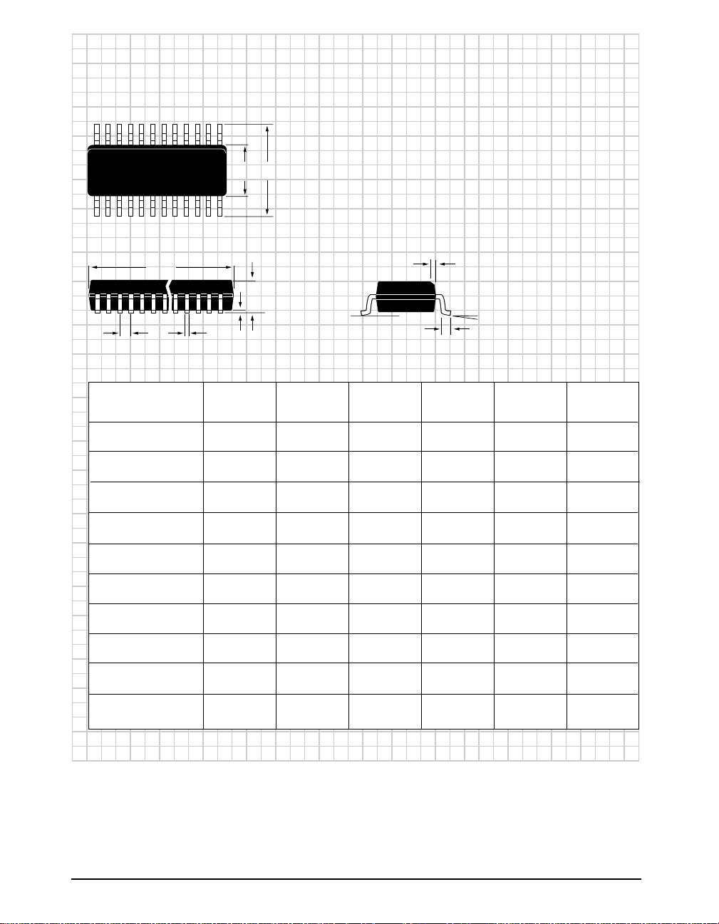
D
Be
DIMENSIONS (Inches)
Minimum/Maximum
(mm)
A
A1
B
D
E
e
H
h
L
Ø
EH
A
A1
8–PIN
0.053/0.069
(1.346/1.748)
0.004/0.010
(0.102/0.249
0.014/0.019
(0.35/0.49)
0.189/0.197
(4.80/5.00)
0.150/0.157
(3.802/3.988)
0.050 BSC
(1.270 BSC)
0.228/0.244
(5.801/6.198)
0.010/0.020
(0.254/0.498)
0.016/0.050
(0.406/1.270)
0°/8°
(0°/8°)
PACKAGE: PLASTIC
h x 45°
14–PIN
0.053/0.069
(1.346/1.748)
0.004/0.010
(0.102/0.249)
0.013/0.020
(0.330/0.508)
0.337/0.344
(8.552/8.748)
0.150/0.157
(3.802/3.988)
0.050 BSC
(1.270 BSC)
0.228/0.244
(5.801/6.198)
0.010/0.020
(0.254/0.498)
0.016/0.050
(0.406/1.270)
0°/8°
(0°/8°)
16–PIN
0.053/0.069
(1.346/1.748)
0.004/0.010
(0.102/0.249)
0.013/0.020
(0.330/0.508)
0.386/0.394
(9.802/10.000)
0.150/0.157
(3.802/3.988)
0.050 BSC
(1.270 BSC)
0.228/0.244
(5.801/6.198)
0.010/0.020
(0.254/0.498)
0.016/0.050
(0.406/1.270)
0°/8°
(0°/8°)
SMALL OUTLINE (SOIC)
(NARROW)
Ø
L
SP9500DS/04 SP9500 12-Bit, Voltage Output D/A Converter © Copyright 2000 Sipex Corporation
8
Page 9
ORDERING INFORMATION
Model .................................................................................. Temperature Range .......................................................................................Package
Monolithic 12-Bit DAC Voltage Output:
SP9500JN ................................................................................ 0˚C to +70˚C .......................................................................... 8-pin, 0.3" Plastic DIP
SP9500KN ............................................................................... 0˚C to +70˚C .......................................................................... 8-pin, 0.3" Plastic DIP
SP9500JS ................................................................................ 0˚C to +70˚C ................................................................................. 8–pin, 0.15" SOIC
SP9500KS ............................................................................... 0˚C to +70˚C ................................................................................. 8–pin, 0.15" SOIC
SP9500AN ............................................................................... –40˚C to +85˚C ...................................................................... 8-pin, 0.3" Plastic DIP
SP9500BN ............................................................................... –40˚C to +85˚C ...................................................................... 8-pin, 0.3" Plastic DIP
SP9500AS ............................................................................... –40˚C to +85˚C ............................................................................. 8–pin, 0.15" SOIC
SP9500BS ............................................................................... –40˚C to +85˚C ............................................................................. 8–pin, 0.15" SOIC
Corporation
SIGNAL PROCESSING EXCELLENCE
Sipex Corporation
Headquarters and
Sales Office
22 Linnell Circle
Billerica, MA 01821
TEL: (978) 667-8700
FAX: (978) 670-9001
e-mail: sales@sipex.com
Sales Office
233 South Hillview Drive
Milpitas, CA 95035
TEL: (408) 934-7500
FAX: (408) 935-7600
Sipex Corporation reserves the right to make changes to any products described herein. Sipex does not assume any liability arising out of the
application or use of any product or circuit described hereing; neither does it convey any license under its patent rights nor the rights of others.
SP9500DS/04 SP9500 12-Bit, Voltage Output D/A Converter © Copyright 2000 Sipex Corporation
9
 Loading...