

Page 1
SP8861
1·3GHz Low Power Single-Chip Frequency Synthesiser
Supersedes version in the1996 Professional Products IC Handbook, HB2480 - 3.0 DS3640 - 4.0 April 1998
The SP8861 is a low power single chip synthesiser
intended for professional radio applications, containing all the
elements (apart from the loop amplifier) required to build a PLL
frequency synthesis loop
The device is serially programmable by a three-wire data
highway and contains three independent buffers to store one
reference divider word and two local oscillator divider words.
A digital phase detector with two charge pumps,
programmable in phase and gain, are provided to improve
lock-up performance. The preset operation of the charge
pumps can be overwritten or the comparison frequencies
switched to output ports under control of the divider word. The
dual modulus ratio and so operating range is also
programmable through the same word.
A power down mode is incorporated as a battery economy
feature.
FEATURES
■ Improved Digital Phase Detector Eliminates
‘Dead Band’ Effects
■ Low Operating Power, Typically 175mW
■ 1·3GHz Operating Frequency
■ Complete Phase Locked Loop
■ High Input Sensitivity
■ Programmed throughThree-Wire Bus
■ Wide Range of Reference Division Ratios
■ Local Storage for Two Frequency Words, giving
Rapid Frequency Toggling
■ Programmable Phase Detector Gain
■ Power Down Mode
4321282726
5
F
*
REF
POWER DOWN
RF INPUT
RF INPUT
*FPD and F
6
7
4
V
EE
8
V
4
CC
9
V
1
CC
10
11
12 13 14 15 16 17 18
outputs are reversed by the phase
REF
detector sense bit in the F1/F2 programming word. The
above diagram is correct when the sense bit is low. See
Table 2 and Fig. 7.
V
1, VEE1 – preamplifier and prescaler supplies
CC
VCC2, VEE2 – oscillator supplies
V
3, VEE3 – charge pump 2 supplies
CC
VCC4, VEE4 – ECL supplies
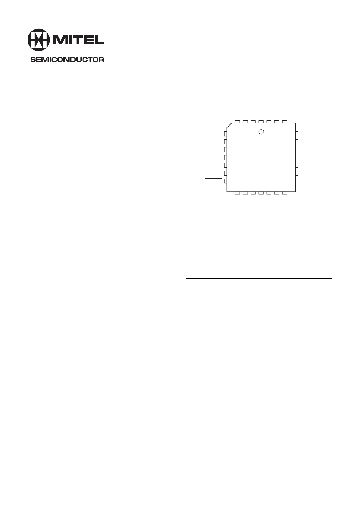
Fig. 1 Pin identification diagram (top view)
*
PD
PD1 OUTPUT
F
SP8861
1
EE
V
F1/F2
3
EE
V
ICCdLOCK DETECT
DATA
CLOCK
NC
ENABLE
NC
2
CC
V
25
24
23
22
21
20
19
PD2 OUTPUT
RPD
3
V
CC
GROUND
XTAL 1
XTAL2
V
2
EE
HP28
ABSOLUTE MAXIMUM RATINGS
Supply voltage
Storage temperature
Operating temperature
Prescaler input voltage
20·3V to 17V
255°C to 1150°C
240°C to 185°C
2·5V p-p
ORDERING INFORMATION
SP8861/NA/HP
Page 2
SP8861
RF INPUT
RF INPUT
F1/F2
DATA
CLOCK
ENABLE
POWER
DOWN
10
11
13
14
15
16
6
DATA
INPUT
16/17 OR 8/9
CONTROL
LOGIC
2-BIT
SR
A COUNT
1LOGIC
4 BIT
N0 N3 N4 N18 N19 N20 N21
N0 N12 N14 N15N13
R
COUNT
REFERENCE
DIVIDER
M COUNT
1LOGIC
15 BIT
22 BIT SHIFT REGISTER
1 BIT13 BIT 2 BIT
*
F
REF
f
PD
DUAL
F1/F2
2 BIT 1 BIT
DATA
BUFFER
SINGLE
REFERENCE
BUFFER
LOGIC
f
REF
and FPD outputs are reversed by the phase detector
PHASE
DETECTOR
CHARGE
PUMP 1
CHARGE
PUMP 2
OUTPUT
INTERFACE
3
24
28
25
27
5
4
PD1
RPD
Cd
PD2
LOCK
DETECT
*
F
REF
FPD*
sense bit in the F1/F2 programming word. The pin allocations
shown are correct when the sense bit is low (see Table 2 and Fig. 7).
21
20
CRYSTAL
f
REF
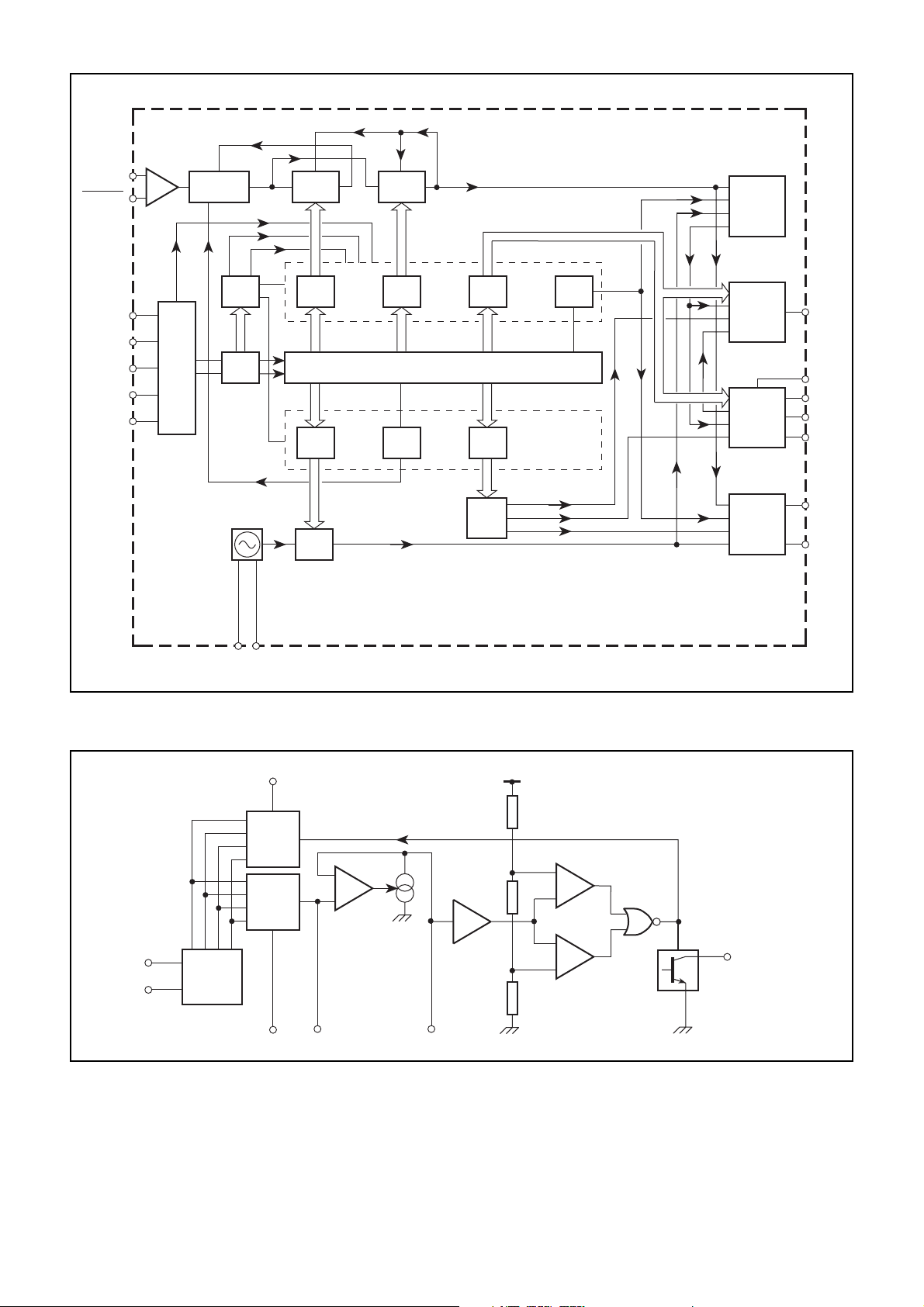
Fig. 2 SP8861 block diagram
V
PD1
3
CHARGE PUMP 1 DISABLE
CHARGE
PUMP 1
(SEE TABLE 4)
−
CHARGE
PUMP 2
f
PD
PHASE
DETECTOR
24
RPD
31
+
TRANSCONDUCTANCE
AMPLIFIER
25
PD2
31
31 BUFFER
28
Cd
CC
Output current at pin 27 is proportional to
voltage difference between pins 25 and 28,
45k
I
= 625µA
MAX
−
10k
45k
+
−
+
DUAL VOLTAGE
COMPARATOR
27
LOCK DETECT
Fig. 3 Detailed block diagram of lock detect circuit
2
Page 3
400
SP8861
350
300
250
200
150
100
INPUT VOLTAGE (mV RMS)
50
25
0
0
GUARANTEED
OPERATING
4
TYPICAL OVERLOAD
WINDOW
8/9 MODE
500
GUARANTEED
OPERATING
WINDOW
4
16/17 MODE
650 750
1000 1300 150015080
FREQUENCY (MHz)
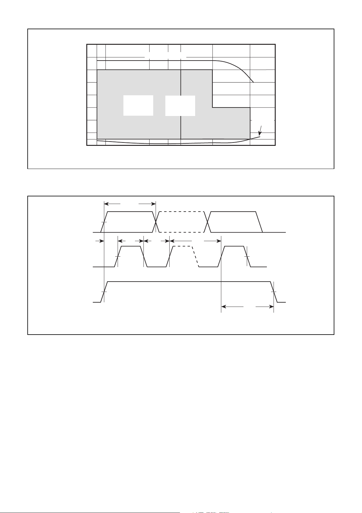
Fig. 4 Typical input characteristics and input drive requirements for SP8861
tS1t
CH
DATA
2V
LAST DATA BITFIRST DATA BIT
TYPICAL
SENSITIVITY
CLOCK
ENABLE
t
REP
t
S
2V
= 1µs min., t
t
CH
= 50ns min., tCH = 50ns min., tCL = 100ns min., tE = 50ns min.
S
t
CL
t
REP
2V
t
E
Fig. 5 Data and clock timing requirements
3
Page 4

SP8861
ELECTRICAL CHARACTERISTICS
These characteristics are guaranteed over the following range of operating conditions unless otherwise stated:
Supply voltage VCC = 14·75V to 15·25V. T
= 255°C to 1125°C (A Grade), 240°C to 185°C (B Grade)
AMB
Characteristic Conditions
Supply current
Supply current in power down mode
Input sensitivity
Input overload
RF input division ratio
Comparison frequency
Reference oscillator input frequency
External reference input voltage
Reference division ratio
Data clock repetition rate, t
Minimum setup time, t
REP
S
DATA input high
DATA input low
CLOCK input high
CLOCK input low
Data ENABLE high
Data ENABLE low
F1/F2 input high
F1/F2 input low
POWER DOWN input high
POWER DOWN input low
F1/F2 input current
POWER DOWN input current
RDP external resistance
LOCK DETECT output voltage when in lock
LOCKDETECT switching voltage high
LOCK DETECT switching voltage low
F
and F
PD
output voltage swing
REF
Pin
8,9,18,23
8
10,11
10,11
10,11,4
4,5
20,21
20
20,5
15
14,15
14
14
15
15
16
16
13
13
6
6
13
6
24
27
25
25
Min.
256
56
10
50
0·6V
V
0·6V
V
0·6V
V
0·6V
V
0·6V
V
68
2·7
4
1
CC
EE
CC
EE
CC
EE
CC
EE
CC
EE
Value
Typ. Max.
33
4·5
40
6
524287
262143
5
20
500
8191
1
V
CC
0·3V
V
CC
0·3V
V
CC
0·3V
V
CC
0·3V
0·9V
0·3V
5
5
330
1
2·3
0·9
CC
CC
CC
CC
CC
CC
Units
mA
mA
MHz
MHz
mVrms
µs
ns
V
V
V
V
V
V
V
V
V
V
µA
µA
kΩ
V
V
V
V
See Fig. 4
See Fig. 4
With 416/17 selected
With 48/9 selected
See Fig. 5
See Fig. 5
F1 buffer selected
F2 buffer selected
V pin 13 = 5·0V
V pin 6 = 4·5V
I pin 27 = 1mA
= 5V
V
CC
= 5V
V
CC
= 5V, external pulldown
V
CC
may be required
4
Page 5
DESCRIPTION
Prescaler and AM Counter
The programmable divider chain is of AM counter design
and therefore contains a dual modulus front end prescaler, an
A
counter which controls the dual modulus ratio and an
M
counter which controls the bulk multi-modulus division.
A programmable divider of this type has a division ratio of
MN1A
and a minimum integer steppable division ratio
of N(N21).
In the SP8861, the dual modulus front end prescaler is a
dual
N
ratio device, capable of being statically switched
between 416/17 and 48/9 ratios. The controlling A counter is
of four-bit design, allowing a maximum count sequence of 15
4
(2
21), which begins with the start of the M counter sequence
and stops when it has counted by the pre-loaded number of
cycles. While the A counter is counting, the dual modulus
prescaler is held in the
N
11 mode then reverts to the N mode
at the completion of the sequence.
The
M
counter is a 15-bit asynchronous divider which
counts with a ratio set by a control word. In both A and
M
counters the controlling data from the F1/F2 buffer is loaded
in sequence with every
M
count cycle. The N ratio of the dual
modulus prescaler is selected by a one-bit word in the
reference divider buffer and, when when a ratio of 48/9 is
selected, the A counter requires only three programming bits,
having an impact on the frequency bit allocation as described
in the data entry section.
Reference Source and Divider
The reference source in the SP8861 is obtained from an
on-chip oscillator which is frequency controlled by an external
crystal. The oscillator can also function as a buffer amplifier to
allow the use of an external reference source. In this mode, the
source is simply AC-coupled into the oscillator transistor base
on pin 20.
The oscillator output is coupled to a programmable reference
counter (
R
) whose output is the reference for the phase
detector. The reference divider is a fully programmable 13-bit
asynchronous design and can be set to any division ratio
between 1 and 8191. The actual division ratio is controlled by
a data word stored in the internal reference buffer.
Phase Detector
The SP8861 contains a digital phase detector which feeds
two charge pump circuits. Charge pump 1 has preset currents
which are programmble as shown in Table 1. Charge pump 2
has a current level set by an external resistor RPD; the current
is multiplied by a factor which is determined by bits G1 and G2
of the F1 or F2 word (see Table 1). Note that charge pump 2
current is pin 24 current 3 muliplication factor, where
V
21·5V
I pin 24 =
A lock detect circuit is connected to the output of charge
pump 2. when the voltage level at pin 25 is between
approximately 2·25V and 2·75V, LOCK DETECT (pin 27) will
be low and charge pump 1 disabled, depending on the PD1
and PD2 programming bits as shown in Table 4.
The output signals from the
on pins 4 and 5 (FPD and F
reference programming word; the various options are shown
in Table 4. An external phase detector may be connected to
pins 4 and 5 and may be used independently or in conjunction
with the on-chip phase detector.
To allow for control direction changes introduced by the
design of the control loop, a control bit in the F1/F2 programming
word interchanges the inputs to the on-chip phase detector
and reverses the functions on pins 4 and 5 (see Table 2).
CC
RPD
R
and M counters are available
) when programmed by the
REF
SP8861
F1 or F2 word
G2 G1
0
1
0
1
0
0
1
1
F1/F2 sense bit Pins 3 and 25 Pin 4
0
1
Data Entry and Storage
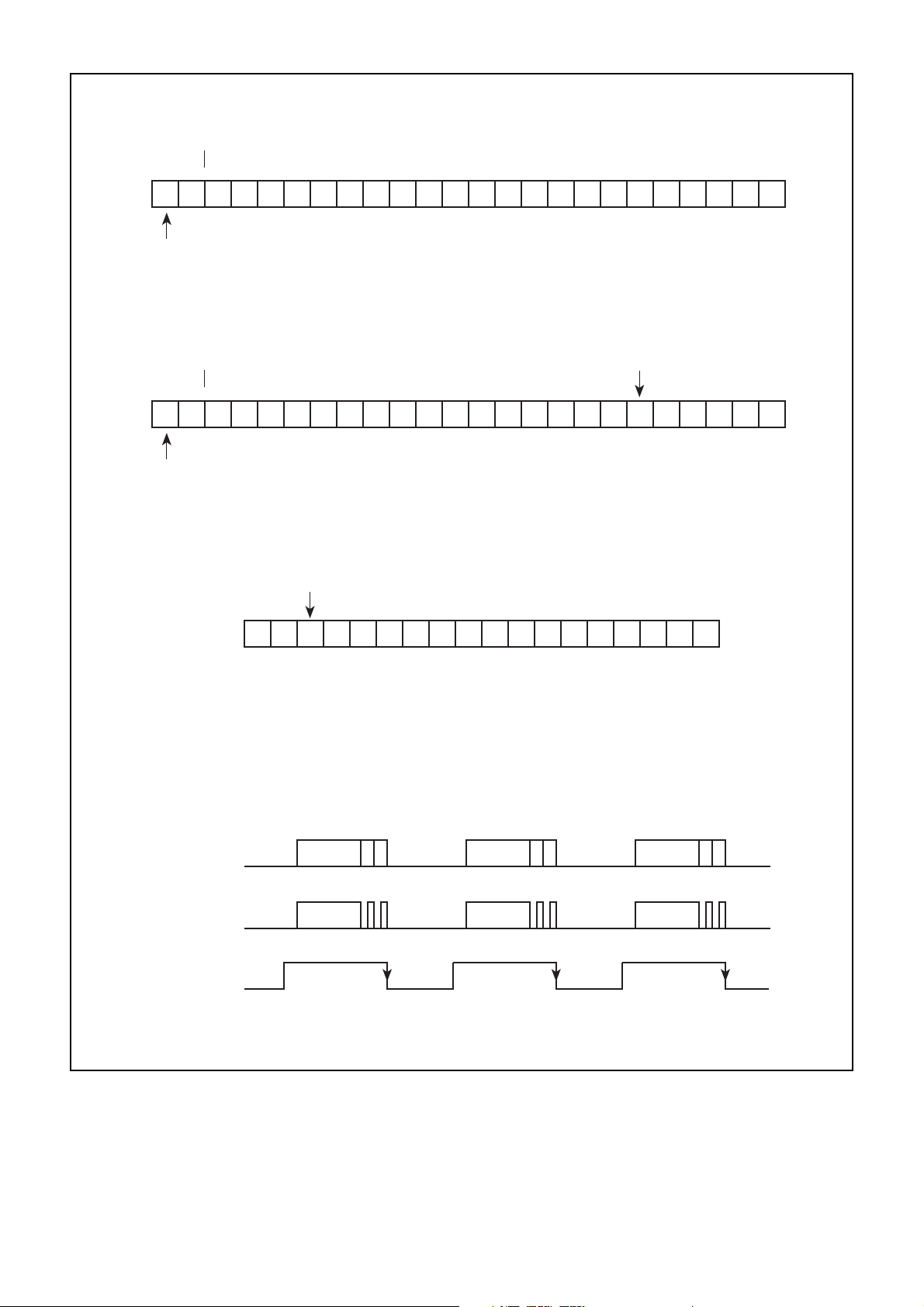
The data section of the SP8861 consists of a data input
interface, a data shift register and three data buffers.
Data is entered to the data input interface via a three-wire
highway, with DATA (pin 24), CLOCK (pin 15) and ENABLE
(pin16) inputs. The input interface routes the data into a 24bit shift register with bus connections to three data buffers.
Data entered via the serial bus is transferred to the appropriate
data buffer on the negative transition of the data enable input
according to the two final data bits C1 and C2 as shown in
Table 3. The MSB of the data is entered first.
2-bit SR contents
C2 C1
0
1
0
1
The dual F1/F2 buffer can receive two 22-bit words and
controls the programmable divider A and M counters using 19
bits, the phase detector gain with two bits and the phase
detector sense with one bit. A fourth input from the synthesiser
control system selects the active buffer.
The third buffer contains only 16 bits, 13 being used to set
the reference divider division ratio and 2 to control the phase
detector enable logic. The remaining bit sets the dual modulus
prescaler
sequence and the shift register can be updated whils the data
buffers retain control of the synthesiser with the previously
loaded data. This enables four unique data words to be stored
in the device, with three in the data buffers and a fourth in the
shift register, while the chip is enabled. The F1 word may also
be updated while F2 is controlling the programmable divider
and vice-versa.
toggled between two frequencies using the F1/F2 select input
at a rate determined by the comparison frequency and also
permits random frequency hopping at a rate determined by a
btye load period; this is possible because the loop can be
locked to F1 while F2 is updated by entering new data via the
shift register. The F1/F2 input is high to select F1.
N
ratio.
The data words may be entered in any individual multiple
The dual F1/F2 buffer enables allows the device to be
Charge pump 1
current (
µA)
Charge pump 2
50
75
125
200
Table 1 Charge pump currents
Output for RF phase lag
Current source
Current sink
F
PD
F
REF
Table 2
Buffer loaded
0
0
1
F1
F2
Transfer A counter bits (N0:N3)
into 4-bit buffer (see Figs. 2 and 7)
1
Reference
Table 3
multiplier
1
1·5
2·5
4
Pin 5
F
F
REF
PD
5
Page 6
SP8861
An F1 or F2 update cycle will consist of a byte containing
24 bits whereas the reference byte will contain 18 bits. The
device requires 3 bytes, each with a chip select sequence,
totalling 66 bits to fully program.
When the dual modulus
A
counter is set to 48/9, the data
required to set the counter is reduced by one bit, leaving an
PD2 PD2 Result
0
1
0
1
0
0
1
1
and FPD outputs off, charge pumps 1 and 2 on
F
REF
and FPD outputs on, charge pump 1 off, charge pump 2 on
F
REF
F
and FPD outputs off, charge pump 1 disabled by lock detect, charge pump 2 on
REF
and FPD outputs on, charge pump 1 disabled by lock detect, charge pump 2 on
F
REF
unused bit in the 22-bit F1/F2 buffer. This bit must always be
set to zero when the 48/9 mode is required. Various
programming sequences are shown in Fig. 7.
The data entry and storage registers are always powered
up, making it possible to enter data when the device is in the
powered down state.
Table 4
F
Rx
Rx
15V
REF
1n
LOOP FILTER
C2
R2
−
+
SL562
V
CC
2
VOLTAGE
15V
C1
CONTROLLED
OSCILLATOR
1n0·1µ
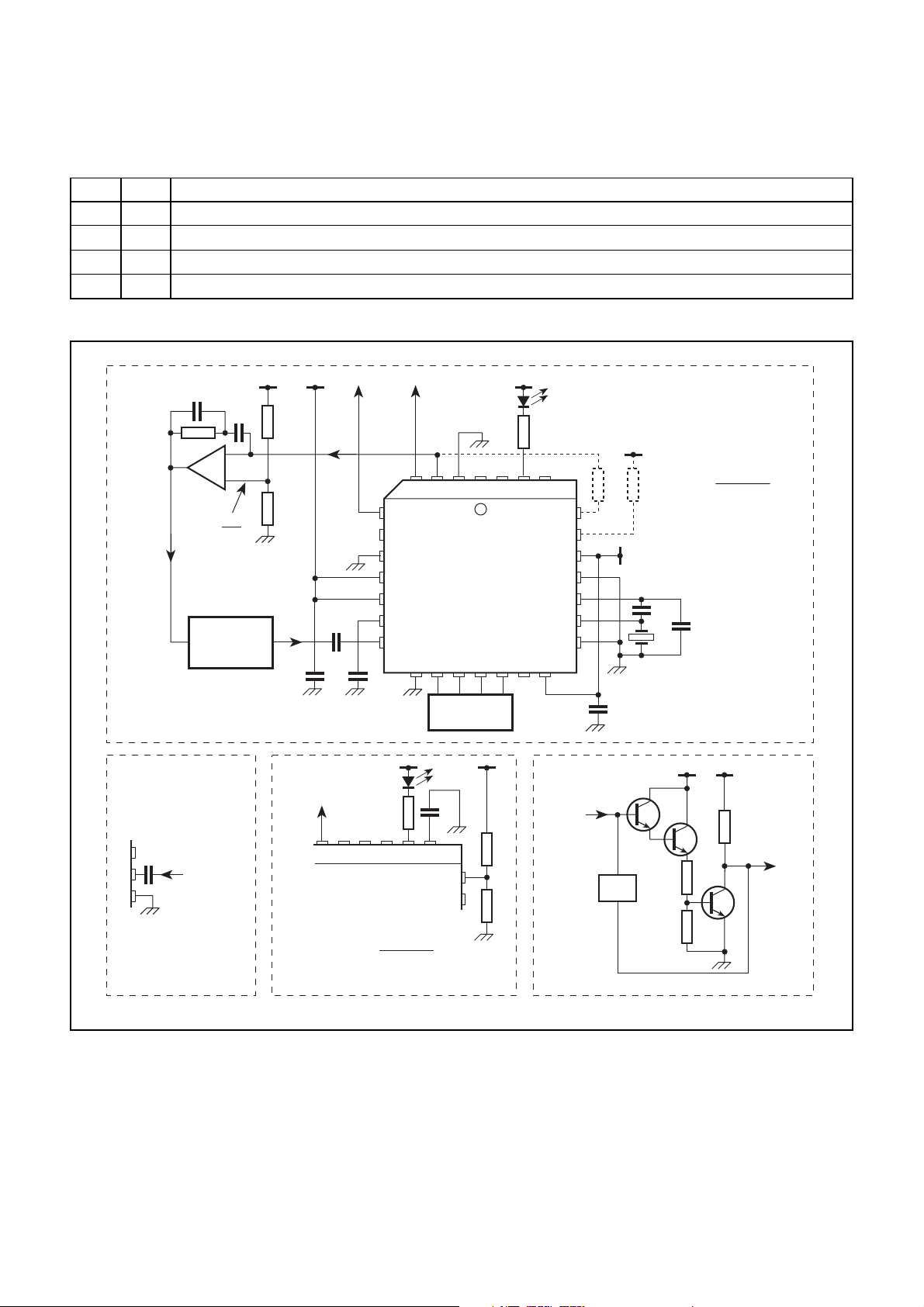
Fig. 6a Typical application
TO LOOP
AMPLIFIER
21
NC
20
19
EXTERNAL
REFERENCE
SOURCE
23
SP8861
Ra
> 23
Fig. 6b Connection
of external reference Fig. 6d Simple discrete amplifier
Fig. 6c Use of lock detect circuit with PD1
F
PD
4321282726
5
6
7
8
9
10
11
12 13 14 15 16 17 18
CONTROL
V
CC
Cd
1282726
25
24
0·25
PD2 current
SP8861
MICRO
V
CC
Ra
Ra
15V
2·2k
FROM
CHARGE
PUMP
25
24
23
22
21
20
19
1n
15V
Rb RPD
15V
LOOP
FILTER
33p
15V
470
22k
Rb
>
39p
10k
0·25
PD2 current
VARICAP
SUPPLY
TO VCO
Fig. 6 Application diagrams
6
Page 7
PHASE
DETECTOR GAIN
CONTROL
(SEE TABLE 1)
MSB LSB
G2 G1 21821721621521421321221121029282726252423222120C2 C1
PHASE
DETECTOR
SENSE BIT
(SEE TABLE 2)
PHASE
DETECTOR GAIN
CONTROL
(SEE TABLE 1)
MSB LSB
G2 G1 2172162152142132122112102928272625242
PHASE
DETECTOR
SENSE BIT
(SEE TABLE 2)
15-BIT PROGRAMMABLE COUNTER (M COUNTER) 4-BIT
Fig. 7a F1 or F2 word, bit allocation with 416/17 selected
15-BIT PROGRAMMABLE COUNTER (M COUNTER) 3-BIT
Fig. 7b F1 or F2 word, bit allocation with 48/9 selected
PROGRAMMABLE
COUNTER
(A COUNTER)
MUST BE ZERO
3
222120C2 C1
0
PROGRAMMABLE
COUNTER
(A COUNTER)
CONTROL
LOGIC
(SEE
TABLE 3)
CONTROL
LOGIC
(SEE
TABLE 3)
SP8861
DATA
DATA CLOCK
CHIP SELECT
DUAL MODULUS
N RATIO SELECT
0 = 416/17
1 = 48/9
MSB LSB
PD1 PD2 21221121029282726252423222120C2C
PHASE
DETECTOR
BISTABLE
CONTROL
(SEE TABLE 4)
13-BIT PROGRAMMABLE COUNTER (R COUNTER)
CONTROL
LOGIC
(SEE
TABLE 3)
Fig. 7c Reference word bit allocation
F1 WORD F2 WORD REF WORD
22 BITS 0 0 22 BITS 1 0 22 BITS 1 1
22 CLOCKS
DATA LOADS ON FALLING EDGES
22 CLOCKS 22 CLOCKS
1
Fig. 7d Data load sequence
Fig. 7 Data format diagrams
7
Page 8
SP8861
VCC1
RF INPUT
RF INPUT
13·25k
10
11
10k
1250 1250
500500
3, 14, 6
0·8mA
VEE1
6k
50µA
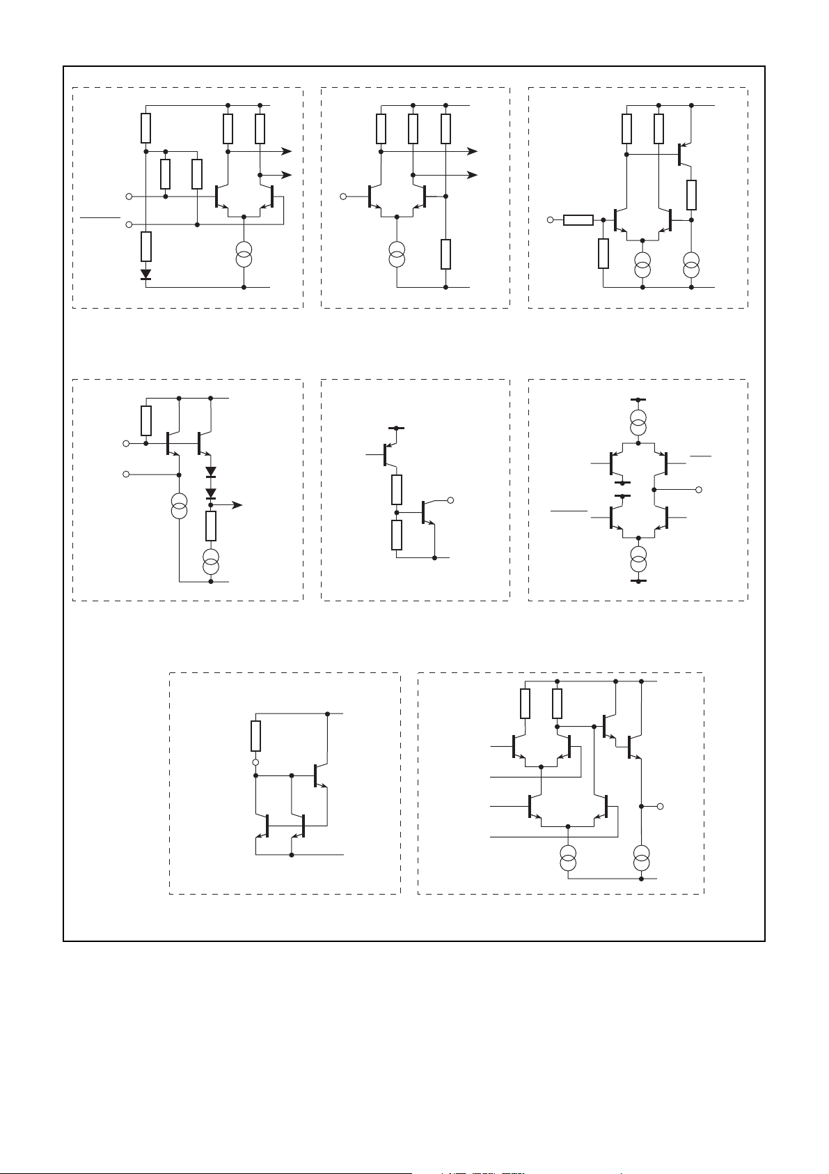
Fig. 8a RF preamplifer inputs Fig. 8b F1/F2 data and
power down inputs
VCC2
24k
20
21
100µA
VCC3
80k
35k
VCC4
6k
62·5k
37·5k
VEE4
15, 16
24k
176k
12k
12k
50µA
VCC4
77·5k
27·5µA
VEE4
Fig. 8c Hysteresis inputs, data clock
and enable
VCC4 (CP1) / VCC3 (CP2)
f
UP
V
DOWN
EE
V
CC
27
f
f
3, 25
f
UP
DOWN
50µA
V
Fig. 8d Oscillator pins
EXTERNAL
RESISTOR
Fig. 8g Charge pump 2 current
2
EE
RPD
(See Table 1)
24
programming
VEE3
Fig. 8e Lock detect output
V
3
CC
FROM M OR R
COUNTERS
OUTPUT
ENABLE
VEE3
Fig. 8h FPD and F
Fig. 8 Input and output interface diagrams
VEE4 (CP1) / VEE3 (CP2)
Fig. 8f Phase detector charge pumps
4
V
CC
10k
4, 5
50µA100µA
VEE4
outputs
REF
8
Page 9

DESCRIPTION
SP8861
A basic application using a single phase detector is shown
in Fig. 6a. The SP8861 is a 1·3GHz part so good RF design
techniques should be employed, including the use of a ground
plane and suitable high frequency capacitors at the RF input
and for power supply decoupling.
The RF input should be coupled to either pin 10 or pin 11,
with the other pin decoupled to ground. The reference oscillator
is of conventional Colpitts type, with two capacitors required to
provide a low impedance tap for the feedback signal to the
transistor emitter. Typical values are shown in Fig. 6a, although
these may be varied to suit the loading requirements of
particular crystals. Where a suitable reference signal already
exists or where a very stable source is required, it is possible
to apply an external reference as shown in Fig. 6b. The
amplitude should be kept below 0·5Vrms to avoid forward
biasing the transistor’s collector-base junction.
Lock Detect and Charge Pump Operation
In some systems, it is useful to have an indication of phase
lock. This function is provided on pin 27 (LOCK DETECT),
which goes low when the output of charge pump 2 (PD2) is
between 2·25V and 2·75V and can be used to drive an LED to
give visual indication of phase lock. Alternatively, a pullup
resistor may be connected from pin 27 to V
used to signal to the control microprocessor that the loop is
locked, thus speeding up system operation. The output current
available from pin 27 is limited to 1·5mA; if this is exceeded,
the logic low level will be uncertain.
The circuit diagram of Fig. 6a is a basic application with
minimum component count but which is neverthless perfectly
adequate for many applications. Charge pump 1 output (pin3)
is used to drive the loop amplifier which provides the control
voltage for the VCO. When charge pump 1 is used in this
mode, the PD1 and PD2 bits in the reference programming
word must be set to enable charge pump 1 continuously (see
Table 4). This application could also use charge pump 2 output
(pin 25) or, if a higher phase detectot gain is required, pins 3
and 25 could be connected in parallel to use the combined
output current from both charge pumps.
The lock detect circuit can be programmed to automatically
disable charge pump 1 as shown in Table 4. This feature can
be used to reduce the system lock up time by connecting the
charge pump outputs in parallel to the loop amplifier with
resistor Rb connected in series with charge pump 2 output.
This connection allows a relatively high current to be used
from charge pump 1 to give a short lock up time, and a low
charge pump 2 current to be set to give low reference frequency
sidebands. The degree of lock up time improvement depends
on the ratio of charge pump 1 and charge pump 2 currents.
When the loop is out of lock, both charge pumps will be
enabled and will feed current to the loop amplifier to bring the
VCO to phase lock. The current from charge 2 will produce a
voltage drop across Rb, allowing operation of the lock detect
circuit and enabling charge pump 1. The value of Rb must be
chosen to give a voltage drop greater than 0·25V at the current
level programmed for charge pump 2. When phase lock is
achieved, there will be no charge pump current and therefore
the voltage at pin 25 will be equal to that on the virtual earth
point of the loop amplifier (2·5V), disabling charge pump 1.
and the output
CC
Charge pump 1 should not be left open circuit when
enabled as this would prevent correct operation of the phase
detector. The output on pin 3 should be biased to half supply
with a pair of 4·7kΩ resistors connected across supplies.
When charge pump 2 is used to drive the loop amplifier, the
lock detect circuit will only give an out of lock indication when
large frequency changes are made or when a frequency
outside the range of the VCO is programmed. at other times
the loop amplifier is maintained at 2·5V by the action of the
loop filter components. Again, a resistor connected between
pin 25 and the loop amplifier, producing a voltage drop greater
than 0·25V at the charge current programmed will allow
sensitive out of lock detection.
When phase lock detection is required using charge
pump 1 only, charge pump 2 output should be biased to 2·5V,
using two equal value resistors, Ra, across the supply as
shown in Fig. 6c. A small capacitor, Cd, connected frompin 28
to ground may be used to reduce chatter at the lock detect
output. A detailed block diagram of the lock detect circuit is
shown in Fig. 3.
Choice of Loop Amplifier
The loop amplifier converts the charge pump current pulses
into a voltage of a magnitude suitable for driving the chosen
VCO. The choice of amplifier is determined by the voltage
swing required at the VCO to achieve the necessary range. In
most cases, an operational amplifier will be used to provide the
essential characteristcs of high input impedance, high gain
and low output impedance required in this application. A
simple discrete design could also be used as shown in Fig. 6d.
This arrangement can be particularly useful where the minimum
VCO control voltage must be close to ground and where
negative supplies are inconvenient. This form of amplifier is
not suitable for use with charge pump 2 when the lock detect
circuit is required.
When an operational amplifier is used in the inverting
configuration shown in Fig. 6a, the charge pump output is
connected directly to the virtual earth point and will therefore
operate a a voltage close to that set on the non-inverting input.
Normally, this operating point should be set at half supply
using a potential divider of two equal value resistors, Rx, but
if necessary the voltage can be set up to 1V higher or lower
without detrimental effect. When the lock detect function is
required on charge pump 2 however, the non-inverting input
must be at half supply.
The digital phase detector and charge pump in the
SP8861 produces bi-directional current pulses in order to
correct errors between the reference and the VCO divider
outputs. Once synchronisation is achieved, in theory no
further output from the charge pump should be required. In
practice, due to leakage currents and particularly the input
current of the amplifier, the capacitors in the loop filter will
gradually discharge, modifying the VCO control voltage and
requiring further outputs from the charge pump to restore
the charge. The effect of this continuous correction is to
frequency modulate the VCO frequency and thus produce
sidebands at the reference frequency. In order to reduce
this effect to a minimum, an amplifier with low input bias is
essential.
9
Page 10
SP8861
C1
R2
−
+
FROM PHASE
DETECTOR
R1
C1
R2
−
+
R3
TO VCO
C2
PHASE
DETECTOR
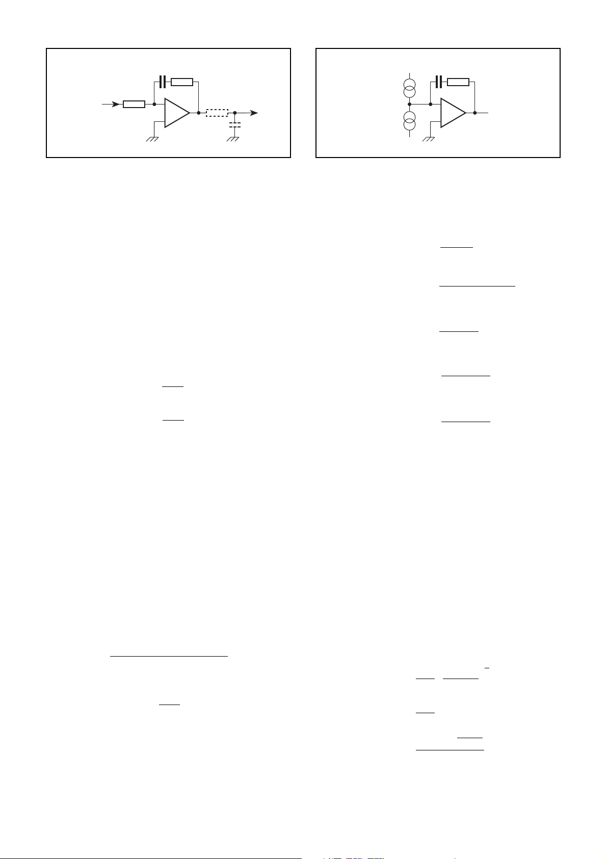
Fig. 9 Standard form of second order loop filter Fig. 10 Modified form of second order loop filter
LOOP CALCULATIONS
Example
Calculate values for a second order loop with the following
Many frequency synthesiser designs use a second order
loop with a loop filter of the form shown in Fig. 9.
In practice, an additional RC time constant (shown dashed
in Fig. 9) is often added to reduce noise from the amplifier. In
addition, any feedthrough capacitor or local decoupling at the
VCO will be added to the value of
C
. These additional
2
components in fact form a third order loop and, if the values
are chosen correctly, the additional filtering provided can
considerably reduce the level of reference frequency sidebands
and noise without adversely affecting the loop settling time.
The calculations of values for both types of loop are shown
below.
Second Order Loop
For this filter, two equations are required to determine the
time constants
where
K
is the phase detector gain factor in V/radian
u
K
is the VCO gain factor = 2p310MHz/V
0
N
is the division ratio from VCO to reference frequency
v
is the natural loop frequency = 500Hz
n
z
is the damping factor = 0·7071
The SP8861 phase detector is a current source rather than
a conventional voltage source and has a gain factor specified
in µA/radian. Since the equations deal with a filter where
is feeding the virtual earth point of an operational amplifier
from a voltage source,
similar to the circuit shown in Fig. 10 – where a current source
phase detector is connected directly to the virtual earth point
of the operational amplifier.
The equivalent voltage gain of the phase detector can be
calculated by assuming a value for
in V/radian which would produce the set current.
The digital phase detector used in the SP8861 is linear
over a range of 2
gain is given by:
For
R
= 1kΩ and assuming a value of phase detector current
1
of 50µA, the phase detector gain is therefore:
This value can now be inserted in equation 1 to obtain a value
for
C
and equation 2 used to determine a value for
1
t
(=
C1R
1
) and t2 (=
1
t
=
1
t
=
2
R
sets the input current to the filter –
1
KuK
v
n
2
v
C1R
); the equations are:
2
0
2
N
z
n
R
and calculating a gain
1
p radians and therefore the phase detector
Phase detector current setting
K
=
u
2p
50µA
K
=
u
p
2
310
3
= 0·00796V/radian
µA/radian
R
…(1)
…(2)
.
2
R
parameters:
Frequency to be synthesised = 800MHz
Reference frequency =100kHz
Division ration
N
800MHz
=
100kHz
= 8000
From equation (1), t1 =
0·079632p310
(2p3500)238310
∴t1 = 6·334µs
t
∴
2
C
1
C
∴
R
2
∴
R
230·7071
2p3500
= 450µs
6·334310
=
= 6·33nF
1
4·5310
=
6·33310
= 71kΩ
2
10
3
From equation (2), t2 =
Now, since t1 =
and, since t2 =
C1R
C1R
,
1
,
2
Third Order Loop
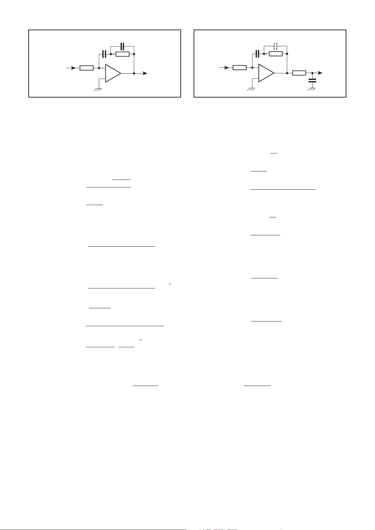
The third order loop is normally as shown in Fig. 11. Fig. 12
shows the circuit redrawn to use an RC time constant after the
amplifier, allowing any feedthrough capacitance on the VCO
line to be included in the loop calculations. Where the modified
form in Fig. 12 is used, it is advantageous to connect a small
capacitor
1
reduce sidebands caused by the amplifier being forced into
non-linear operation by the phase comparator pulses
constants
for Fig. 11
and for Fig. 12
The equations are:
C
of typically 100pF (shown dashed) across
X
Three equations are required to determine the time
t
, t2, and t3, where
1
t
=
C1R
1
t
2
t
3
t
t
t
t
t
t
=
=
=
1
=
2
=
3
=
1
=
2
=
3
1
R
(
C
2
C2R
2
C1R
1
C1R
2
C2R
3
KuK
0
2
v
N
n
1
2
2
v
t
n
3
2tan F
1
C
)
1
2
2
0
v
v
1
cos F
n
2
t
n
2
2
2
t
n
3
1
11
11
v
24
29
6
3
26
R
to
2
1
2
…(3)
…(4)
0
…(5)
10
Page 11
SP8861
C2
C1
FROM
CHARGE
PUMP
R1
R2
−
+
TO VCO
Fig. 11 Standard form of third order loop filter Fig. 12 Modified form of third order loop filter
where
K
,
K
,
N
and
v
u
loop and F
values can now be substituted in equation (3) to obtain a value
C
for
and
R
0
is the phase margin, normally set to 45°. These
0
and in equations (4) and (5) to determine values for
1
.
2
are as defined for the second order
n
C
Example
Calculate values for a third order loop with parameters as
for the second order loop and F
From equation (5):
2tan 45°1
t
=
3
0·4142
=
3161·6
∴t
= 131·8µs
3
= 45°.
0
cos 45°
500Hz32
1
p
From equation (4):
1
24
∴t
t
=
2
(500323p)231·318310
= 768·7µs
2
Using these values in equation (3):
3[A]
25
1
2
2
2
Now, since
t
1
where A =
t
1
∴t
1
t
=
C1R
1
C
∴
7·963102332p310MHz/V
=
80003(50032p)
2
11
11
11(50032p)23(7·68731024)
=
11(50032p)23(1·31831024)
500141·6 6·832
=
7·896110
= 6·3343102632·415
2
v
t
n
2
2
2
v
t
n
3
10
1·1714
2
1
2
= 15·3µs
and
R
1
= 0·0153µF
1
=1kΩ,
1
C
1
1·53310
=
10
3
Cx
C1
FROM
CHARGE
PUMP
For Fig. 11, t2 =
For Fig. 12,
2
Substituting for
For Fig. 12,
Since the values of
or,
or,
or,
R1
t
C
:
2
t
R
∴
R
t
∴
C
t
C
∴
C
t
R
∴
R
t
R
=
C2R
3
=
R
2
2
t
=
2
7·6873102421·318310
=
= 41·627kΩ
2
=
C2R
3
1·318310
=
= 3·17nF
2
=
C1R
1
1·53310
=
1
= 0·0153nF
1
=
C1R
2
7·687310
=
2
1·53310
= 50·242kΩ
2
=
C2R
3
C
2
−
+
(
C
1
2
1
2
C
1
1
22t3
C
1
0·0153310
=
2
41627
1
3
10
2
3
and
R2
R3
C
)
2
t
3
=
R
C
2
R
2
t
3
R
2
24
25
24
28
R
are independent of the other
3
11t3
24
26
components, either can be chosen and the other determined.
Assuming that
R
= 1kΩ, then
3
1·318310
C
=
2
∴
C
= 0·01318µF
2
10
24
3
TO VCO
C3
11
Page 12
Page 13

http://www.mitelsemi.com
World Headquarters - Canada
Tel: +1 (613) 592 2122
Fax: +1 (613) 592 6909
North America Asia/Pacific Europe, Middle East,
Tel: +1 (770) 486 0194 Tel: +65 333 6193 and Africa (EMEA)
Fax: +1 (770) 631 8213 Fax: +65 333 6192 Tel: +44 (0) 1793 518528
Fax: +44 (0) 1793 518581
Information relating to products and services furnished herein by Mitel Corporation or its subsidiaries (collectively “Mitel”) is believed to be reliable. However, Mitel assumes no
liability for errors that may appear in this publication, or for liability otherwise arising from the application or use of any such information, product or service or for any infringement of
patents or other intellectual property rights owned by third parties which may result from such application or use. Neither the supply of such information or purchase of product or
service conveys any license, either express or implied, under patents or other intellectual property rights owned by Mitel or licensed from third parties by Mitel, whatsoever.
Purchasers of products are also hereby notified that the use of product in certain ways or in combination with Mitel, or non-Mitel furnished goods or services may infringe patents or
other intellectual property rights owned by Mitel.
This publication is issued to provide information only and (unless agreed by Mitel in writing) may not be used, applied or reproduced for any purpose nor form par t of any order or
contract nor to be regarded as a representation relating to the products or services concerned. The products, their specifications, services and other information appearing in this
publication are subject to change by Mitel without notice. No warranty or guarantee express or implied is made regarding the capability, performance or suitability of any product or
service. Information concerning possible methods of use is provided as a guide only and does not constitute any guarantee that such methods of use will be satisfactory in a specific
piece of equipment. It is the user’s responsibility to fully determine the performance and suitability of any equipment using such information and to ensure that any publication or
data used is up to date and has not been superseded. Manufacturing does not necessarily include testing of all functions or parameters. These products are not suitable for use in
any medical products whose failure to perform may result in significant injury or death to the user. All products and materials are sold and services provided subject to Mitel’s
conditions of sale which are available on request.
M Mitel (design) and ST-BUS are registered trademarks of MITEL Corporation
Mitel Semiconductor is an ISO 9001 Registered Company
Copyright 1999 MITEL Corporation
All Rights Reserved
Printed in CANADA
TECHNICAL DOCUMENTATION - NOT FOR RESALE
 Loading...