

Page 1
SP8858
1·5GHz Professional Synthesiser
Supersedes March 1997 version, DS3843 - 3.0 DS3843 - 4.1 July 1998
The SP8858 is a single chip synthesiser intended for PLL
signal synthesis applications up to 1.5GHz and includes a
dual modulus prescaler (4N/N11), programmable A, M and
R dividers, digital phase detector, charge pump and lock
detect circuits.
The SP8858 is a development of the SP8853 synthesiser
with low residual phase noise, increased dynamic range
above 1GHz and an improved high gain phase detector
design that eliminates the dead-band.
The low prescaler modulus, programmable to either 16/17
or 8/9, together with the 15-bit M counter and 13-bit reference
counter make this device ideal for a diverse range of high
performance applications.
The nominal phase detector gain is set by a reference
current into pin 24 and the gain can be varied over a 4:1 range
when the device is programmed. The dividers, the phase
detector sense, the prescaler modulus and the data buffer
control logic are also programmable using the three wire
serial interface. An alternative 22-bit control word for the A
and M dividers and phase detector gain can be stored so
allowing fast frequency hopping and bandwidth switching by
simply toggling the logic level on pin 13 (F1/F2). In addition,
the A counter of the ‘active’ buffer can be programmed with
only 6 bits, allowing fast hopping to adjacent channels.
A simple exclusive - or lock detect circuit is also provided,
the sensitivity of which is determined by an external capacitor.
FEATURES
■ Low Residual Phase Noise (see Reference 1)
■ Operation to 1·5GHz over Full Temperature Range
■ High Input Sensitivity
■ Improved Linear Digital Phase Detector
■ Programmable Charge Pump Current: 10µA to 2 mA
■ On-chip 416/17 or 48/9 Dual Modulus Prescaler
■ Three-wire Serial Data Interface
■ 13-bit Reference Counter
■ 15-bit M Counter
■ Stores an Alternative Programming Word
■ Facility to Program A counter Only
■ Power Saving Standby Mode
F
REF
POWER DOWN
4
V
EE
4
V
CC
1
V
CC
RF INPUT
RF INPUT
F
REF
POWER DOWN
4
V
EE
4
V
CC
1
V
CC
RF INPUT
RF INPUT
4321282726
5
*
6
7
8
9
10
11
12 13 14 15 16 17 18
5
*
6
7
8
9
10
11
12 13 14 15 16 17 18
3
*
EE
PD
NC
V
F
1
EE
V
*
PD
F
4321282726
NCCDLOCK DETECT
SP8858
F1/F2
DATA
CLOCK
ENABLE
3
EE
NC
V
NCCDLOCK DETECT
NC
CP REF
25
24
23
22
21
20
19
2
CC
V
CP REF
SP8858
1
EE
V
F1/F2
DATA
CLOCK
NC
ENABLE
2
CC
V
25
24
23
22
21
20
19
CP OUTPUT
RPD
3
V
CC
GROUND
XTAL 1
XTAL2
2
V
EE
HC28
CP OUTPUT
RPD
3
V
CC
GROUND
XTAL 1
XTAL2
2
V
EE
HP28
ABSOLUTE MAXIMUM RATINGS
Supply voltage
Storage temperature
Operating temperature
Prescaler input voltage
20·3V to 17V
265°C to 1150°C
255°C to 1125°C
2·5V p-p
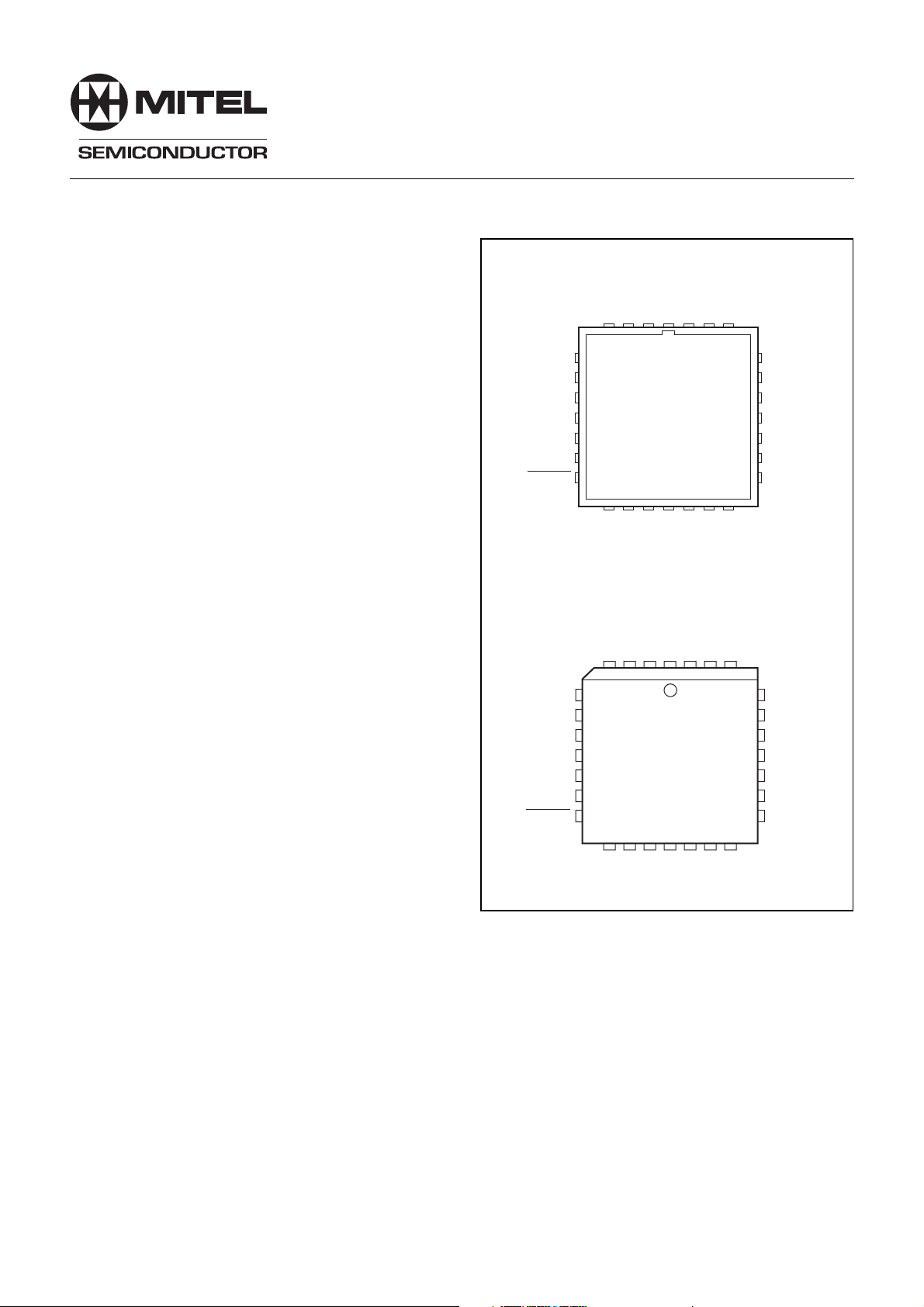
Fig. 1 Pin connections (top view)
ORDERING INFORMATION
SP8858 IG HCAR 240°C to 185°C (Industrial grade)
SP8858 MG HCAR 255°C to 1125°C (Military grade)
SP8858 IG HPAS 240°C to 185°C (Industrial grade)
Page 2

SP8858
Pin Description
F
4
= M divider output pulses = RF input frequency 4(MN1A) when SENSE bit in the programming
PD
word = ‘0’. When SENSE bit = 1, this pin is F
= R divider output pulses = reference input
REF
frequency 4R. (see Data Entry and Control description and Fig. 6).
F
5
= R divider output pulses when SENSE bit in the programming word = ‘0’. When SENSE
REF
bit = 1, this pin is FPD = M divider output pulses (see Data Entry and Control description and
Fig. 6).
6 (POWER DOWN)
10, 11 (RF INPUT)
13 (F1/F2)
14 (DATA)
15 (CLOCK)
16 (ENABLE)
20 (XTAL 2)
21 (XTAL 1)
24 (RPD)
25 (CP OUTPUT)
With this pin held high the device is in the power saving standby mode. The serial interface shift
register and data buffers remain active at all times so that the device can still be programmed in
this mode.
Balanced inputs to the RF preamplifier. For single ended operation the signal is AC coupled into
pin 11 with pin 10 decoupled to ground or vice-versa.
The logic level on this input determines which of the two words stored in the internal buffers is used
to reload the A and M dividers at the end of the count cycle. With F1/F2 high the F1 buffer is selected.
Serial data on this line is clocked into a shift register under control of CLOCK and ENABLE.
Clocks the data into the shift register.
Logic high on this pin allows data to be clocked into the shift register and the subsequent falling edge
loads the buffer chosen by the LSBs of the programmed word. The clock input is ignored when
ENABLE is low.
This pin is the input to a buffer amplifier if an external reference signal is provided. Alternatively,
the amplifier provides the active element for a reference oscillator if a quartz crystal is connected
at this point (see Applications).
Leave open circuit if an external reference is used or connect load capacitors for the chosen crystal
(see Applications)
An external resistor connected between this pin and V
sets the charge pump output current. A
CC
multiplication factor can also be programmed into the device (see Table 3)
The phase detector output is a single-ended charge pump sourcing or sinking current to the
inverting input of an external loop filter.
26 (CP REF)
27 (LOCK DETECT)
28 (CD)
9 (V
1), 12 (VEE1)
CC
18 (V
2), 19 (VEE2)
CC
23 (VCC3), 2 (VEE3)
8 (V
4), 7 (VEE4)
CC
2
Connected to the non-inverting input of the loop filter to set the DC bias.
A current sink into this pin is enabled when the lock detect circuit indicates lock. Used to give
external indication of phase lock.
A capacitor connected to this point determines the lock detect integrator time constant and can be
used to vary the sensitivity of the phase lock indicator.
Pre-amp and prescaler supply.
Oscillator supply.
Charge pump supply.
ECL supply.
Table 1 Pin descriptions
Page 3
MODULUS CONTROL
SP8858
RF INPUT
RF INPUT
F1/F2
DATA
CLOCK
ENABLE
POWER
DOWN
10
11
13
14
15
INTERFACE
16
6
16/17 OR 8/9
DATA
V
REF
20
CRYSTAL
COUNTER
XFV
3 BITS SELECT F1/F2
SELECT MODULUS
SELECT R
XFR
ACTIVE A
C1 C2
LSB MSB
DIVIDER
*
F
REF
sense bit in the F1/F2 programming word. The pin allocations
shown are correct when the sense bit is low (see Fig. 6).
21
f
4 BITS
PD
PD GAIN
2 BITS
PD1 PD2
DECODE
FV
XFV
FR
XFR
PHASE
DETECTOR
BUFFER
DISABLE
FV
A
COUNTER
22 BITS
16 BITS
FR
M
RESET
15 BITS
F1/F2 22-BIT DATA BUFFER
24-BIT SHIFT REGISTER
16-BIT REFERENCE BUFFER
13 BITS
R
and FPD outputs are reversed by the phase detector
LOCK
DETECT
PD
SENSE
CHARGE
PUMP
28
CD
27
LOCK
DETECT
24
RPD
25
CP OUTPUT
25
CP REF
4
FPD*
5
F
REF
*
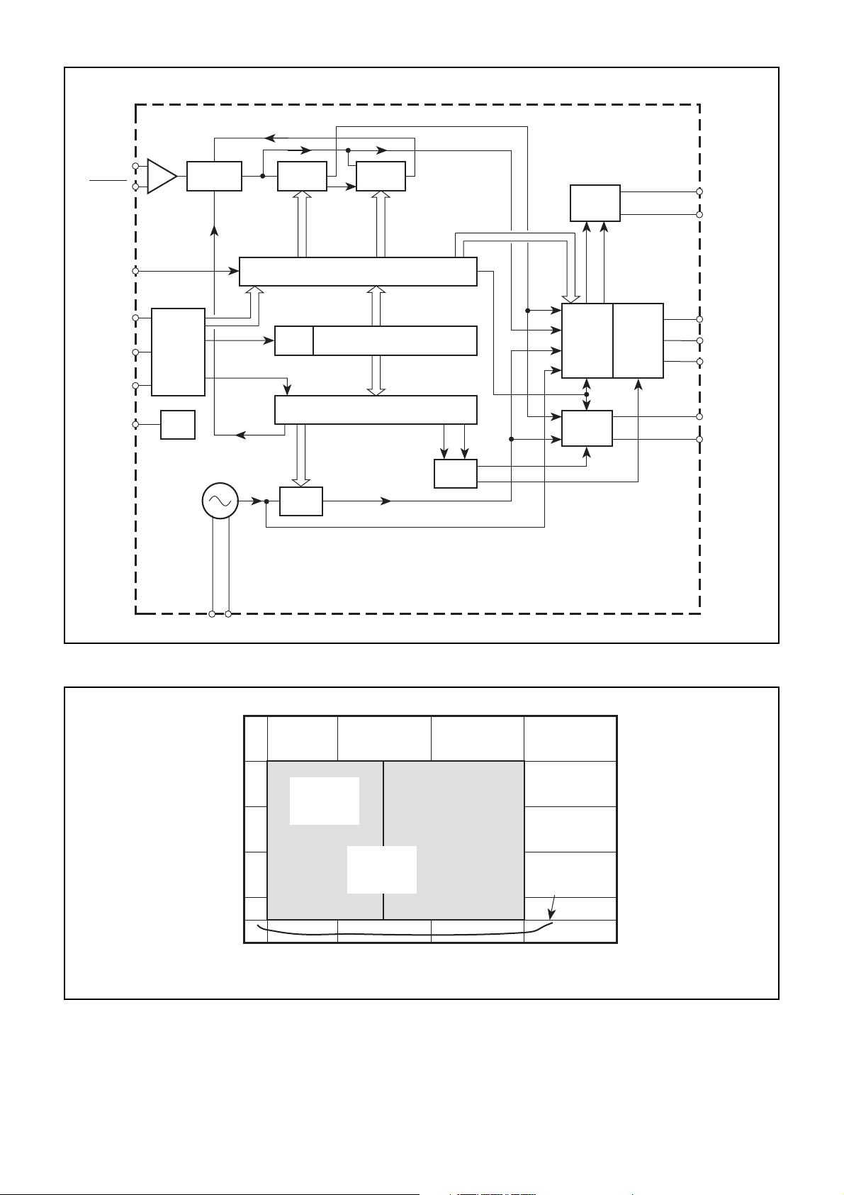
Fig. 2 SP8858 block diagram
500
400
GUARANTEED
300
200
INPUT VOLTAGE (mV RMS)
100
50
0
0
OPERATING
WINDOW
4
8/9 MODE
500
GUARANTEED
OPERATING
WINDOW
4
16/17 MODE
750
1000 150080
FREQUENCY (MHz)
Fig. 3 Typical input characteristics and input drive requirements
TYPICAL
SENSITIVITY
3
Page 4

SP8858
ELECTRICAL CHARACTERISTICS
These characteristics are guaranteed over the following range of operating conditions unless otherwise stated:
Supply voltage VCC = 14·75V to 15·25V. T
= 255°C to 1125°C (Military), 240°C to 185°C (Industrial)
AMB
Characteristic Conditions
Supply current
Supply current in power down mode
Input sensitivity
Input overload
RF input division ratio
Comparison frequency
Reference oscillator input frequency
External reference input voltage
Reference division ratio
Data clock repetition rate, t
Minimum setup time, t
REP
S
DATA input high
DATA input low
CLOCK input high
CLOCK input low
ENABLE high
ENABLE low
F1/F2 input high
F1/F2 input low
POWER DOWN input high
POWER DOWN input low
F1/F2 input current
POWER DOWN input current
Current into RPD
Charge pump current
Charge pump current accuracy
Charge pump leakage
LOCK DETECT output voltage when in lock
F
and F
PD
output voltage swing
REF
Pin
8,9,18,23
8
10,11
10,11
10,11,4
4,5
20,21
20
20,5
15
14,15
14
14
15
15
16
16
13
13
6
6
13
6
24
25
25
25
27
27
Min.
400
240
56
50
50
0·6V
V
0·6V
V
0·6V
V
0·6V
V
0·6V
V
50
4
1
CC
EE
CC
EE
CC
EE
CC
EE
CC
EE
Value
Typ. Max.
95
35
110
45
50
524287
262143
5
40
600
8191
200
V
CC
0·3V
V
CC
0·3V
V
CC
0·3V
V
CC
0·3V
0·9V
0·3V
5
5
500
2
65
2
5
1
0·9
CC
CC
CC
CC
CC
CC
Units
mA
mA
mVrms
mVrms
MHz
MHz
mVrms
ns
ns
V
V
V
V
V
V
V
V
V
V
µA
µA
µA
mA
%
µA
V
See Fig. 3
See Fig. 3
With 416/17 selected
With 48/9 selected
See note 1
See Fig. 4
See Fig. 4
F1 buffer selected
F2 buffer selected
V pin 13 = 5·0V
V pin 6 = 4·5V
500µA34
Charge pump current = 2mA
I pin 27 < 3mA
= 5V, external pulldown
V
CC
may be required
LOCK DETECT output resistor
NOTE 1. The reference frequency range when using a crystal oscillator is 4-20MHz.
27
50
4
kΩ
Page 5
tS1t
SP8858
CH
DATA
CLOCK
ENABLE
t
t
S-EN
2V
S
2V
t
CH
t
REP
t
S
t
CH
t
CL
t
E
t
S-EN
t
CL
t
REP
= tCH 1 tCL MIN
= 50ns MIN
= 100ns MIN
= 100ns MIN
= 50ns MIN
= [(31M)N1A]4RF INPUT (Hz)150ns
OR 14REFERENCE (Hz)150ns
WHICHEVER IS APPROPRIATE
(SEE DATA ENTRY AND CONTROL)
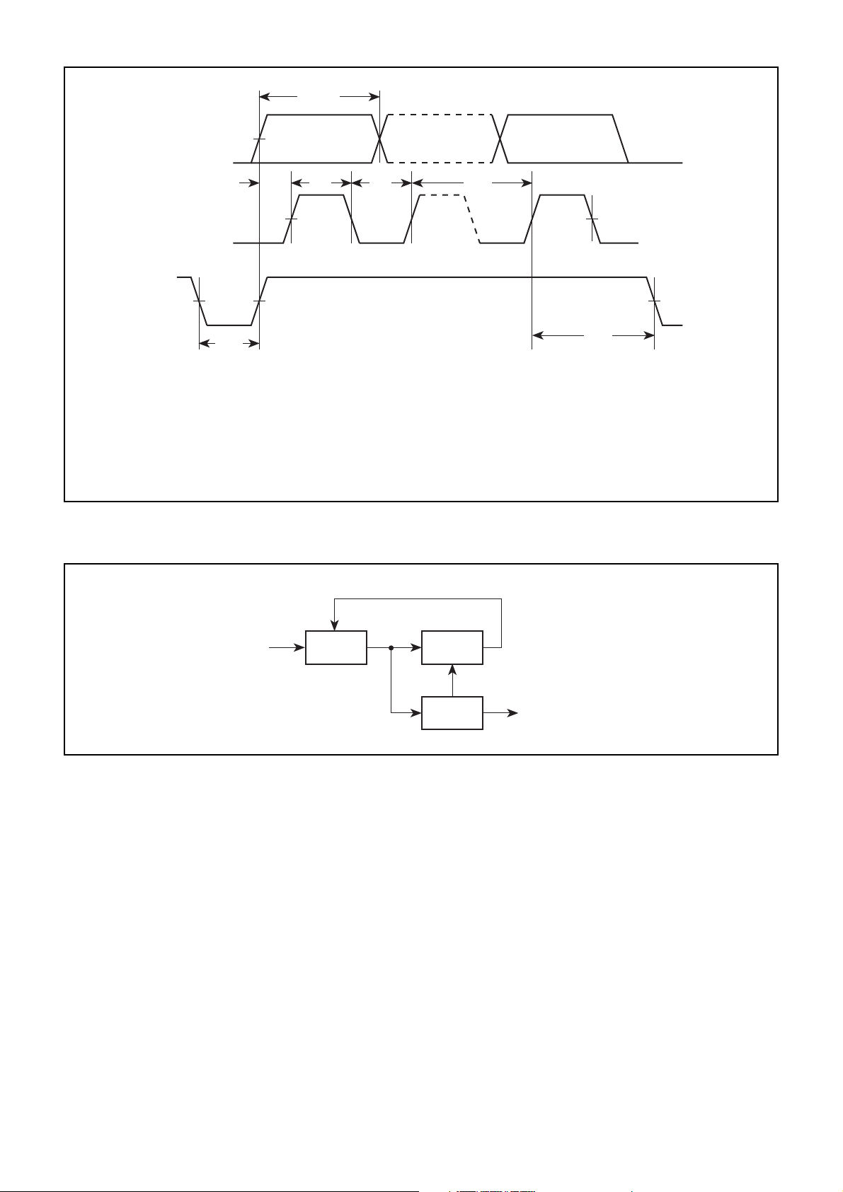
Fig. 4 DATA, CLOCK and ENABLE timing requirements
LAST DATA BITFIRST DATA BIT
2V
t
E
RF INPUT
PRESCALER
4
N / N11
MODULUS CONTROL
A
COUNTER
RESET
M
COUNTER
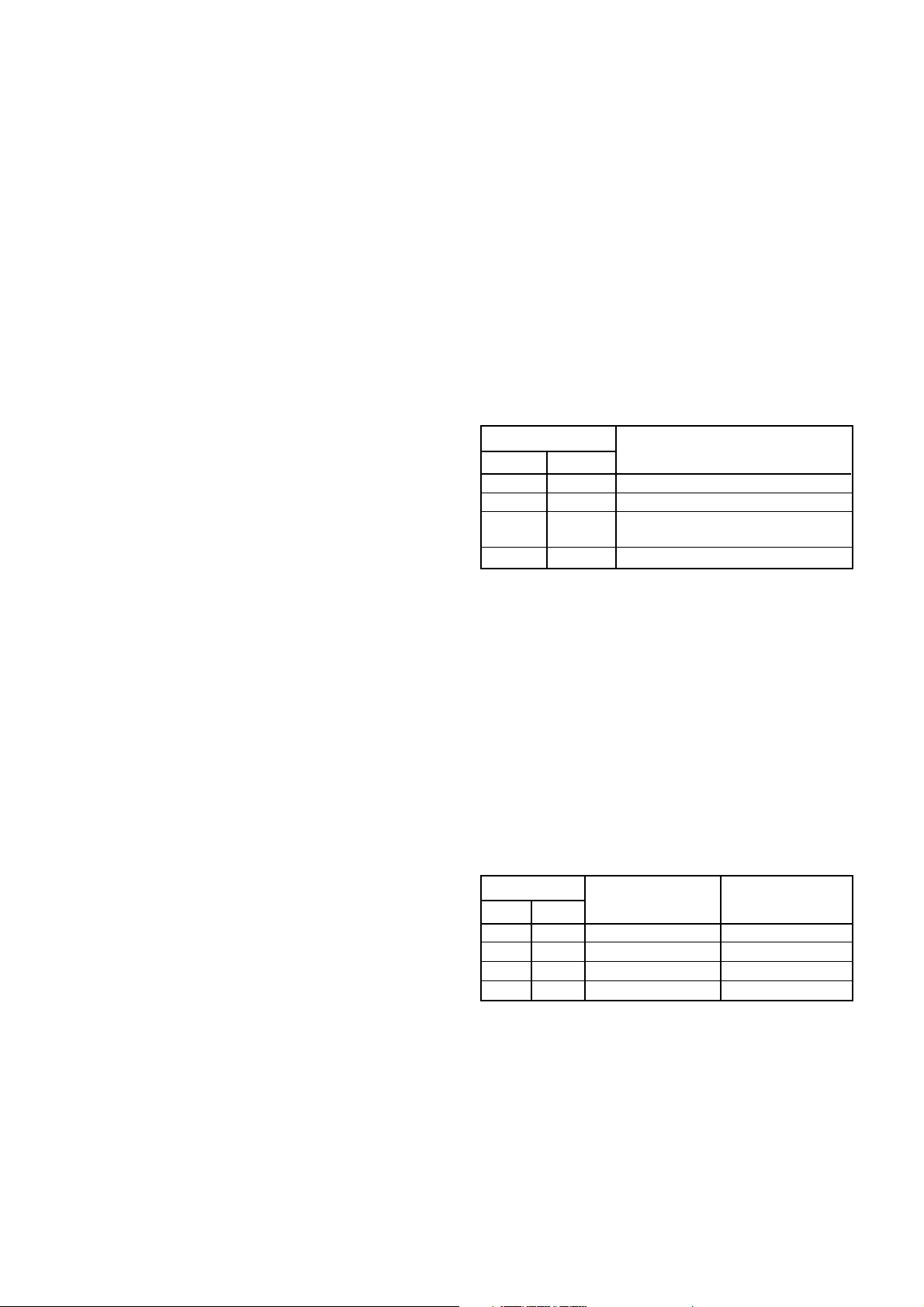
Fig. 5
RF INPUT 4(MN1A)
5
Page 6
SP8858
DESCRIPTION
Prescaler and Dividers
The block diagram of a dual modulus divider arrangement
is shown in Fig. 5. The N/N11 prescaler, together with the
A and M dividers, divide the RF input frequency down to the
comparison frequency at the phase detector input. The
comparison frequency, F
loop synthesiser; when A is incremented (or decremented) by
one, the loop output frequency automatically increments (or
decrements) by F
Hz. When the dividers are reset, at the
REF
end of each count cycle, the modulus of the prescaler is set
to N11 and the input frequency to the A and M dividers is then
RFinput 4(N11) Hz. The output of the A counter controls the
prescaler modulus, which is set to N when A reaches its
programmed value. The M divider continues to count at the
rate RFinput 4N until it reaches its programmed value, at
which point the dividers are reset and the count cycle starts
again. The division ratio of this arrangements is therefore
A(N11) 1 (M2A)N = MN1A
It is evident that for this arrangement to work M must
always be programmed greater than or equal to A and A must
be able to count to N21. These restrictions set a minimum
count of N
2
2N; below this value some division ratios will not
be available.
The SP8858 prescaler can be set to 48/9 or 416/17 mode
by setting the appropriate bit of the reference word. The
A divider is a 4-bit counter, whilst the M divider is a 15-bit
counter. The minimum division ratio, with the 8/9 prescaler, is
2
8
28 = 56, whilst the maximum division ratio, with the 16/17
prescaler, is 16(2
15
21)1(2421) = 524287.
If the 8/9 prescaler is used the MSB of the A counter must
be programmed to 0 and the maximum RF input frequency
must be reduced to 750MHz.
Reference Source and Divider
The reference source for the SP8858 is obtained from an
on-chip oscillator, stabilised by an external quartz crystal. The
oscillator circuit will also function as a buffer amplifier if an
external reference is preferred. In the latter case the signal,
should be AC coupled into pin 20 (see Fig. 12).
The reference oscillator drives a divider stage, the output
of which is the reference signal to the phase comparator. The
PLL controls the input voltage to an external VCO so that the
divided VCO signal is phased locked to this reference signal.
The dynamics of the control loop are determined by the
external loop filter.
The 13-bit reference divider is fully programmable and can
be set to any ratio between 1 and 8191. The programmed
word is stored in the internal reference buffer.
, sets the resolution of a single
REF
reference current into pin 24 (RPD). An external
transimpedance amplifier is required to provide the voltage
drive to the VCO. This requirement is usually performed by
the loop filter operational amplifier which is designed to
provide a type II third order control loop.
Data Entry and Control
The SP8858 is programmed using the serial data interface.
Data is entered into the chip on the DATA pin and clocked into
the internal shift register by the positive going edge of the
CLOCK signal with the ENABLE pin held high. While ENABLE
is high, changes to the shift register will not affect the current
count cycle. On the falling edge of ENABLE the data held in
the shift register is transferred to one of the three buffers (F1,
F2 or reference). Fig. 4 shows the timing requirements for
these three signals.
The 2 LSBs of the 24-bit shift register, C1 and C2, determine
which of the three buffers is loaded with the data held in the
remaining 22 bits as shown in Table 2.
2-bit SR contents
C2 C1
0
1
0
0
0
1
F1
F2
Active A (only the A divider of the
active buffer is changed)
1
1
Reference
Table 2
If the F1 buffer (C2 = 0, C1 = 0) is selected the 22 MSBs
of the shift register are transferred to it. 19 bits of the buffer
provide the data for the A and M dividers; the three remaining
bits control the charge pump current multiplication factor and
the sense of the phase detector. The F2 buffer performs the
same function so that an alternative divider word and/or
phase detector gain can be stored.
The CP current can be multiplied by up to four times by
programming bits G1 and G2 as shown in Table 3. The
maximum charge pump output current is 62mA.
The reference current can be set by resistor RPD
connected between V
Ipin 24 = (V
I
= G3Ipin 24 (G is multiplication factor)
OUT
CC
and pin 24 so that:
CC
21·5)/RPD
Phase detector gain, KPD = I
See Applications, Loop Filter Design
Buffer loaded
/2p A/rad
OUT
Phase Comparator and Charge Pump
The digital phase detector is sensitive to frequency and
phase errors. The basic circuit for a conventional digital
phase/frequency detector is based on two D type flip-flops.
Initially the flip-flops are reset, each one is then set by the
respective pulses of the M and R divider outputs. When both
flip-flops have been set they are immediately reset. In this way
the output of one flip-flop is a pulse whose width is proportional
to phase difference, whilst the second flip-flop is a narrow
pulse determined by the time to reset. The phase detector
outputs drive a charge pump amplifier. One output controls a
constant current source, the other an identical current sink
connected to the same node (CP output, pin 25). The SP8858
phase/frequency detector has been modified and improved to
provide a linear characteristic, thus eliminating deadband
effects.
The phase detector gain is determined by the output
current from the charge pump (±I
) which is set by a
OUT
6
F1 or F2 word
G2 G1
0
1
0
1
0
0
1
1
Charge pump 1
current (
µA)
50
75
125
200
Charge pump 2
multiplier
1
1·5
2·5
4
Table 3 Charge pump currents
When the SENSE bit is set to 1 the inputs and clocks to the
phase detector flip-flops are reversed. The bit should be set
to 1 for a VCO with a positive frequency v. voltage characteristic.
The sense bit also swaps the outputs FREF and FPD on pins
4 and 5. Fig. 1 shows the pin-out for SENSE = 0.
The active buffer, i.e. the one that is currently used to
update the dividers, is selected at pin 13 (F1/F2). A high on
this pin selects F1. The F2 word can be updated while F1 is
Page 7
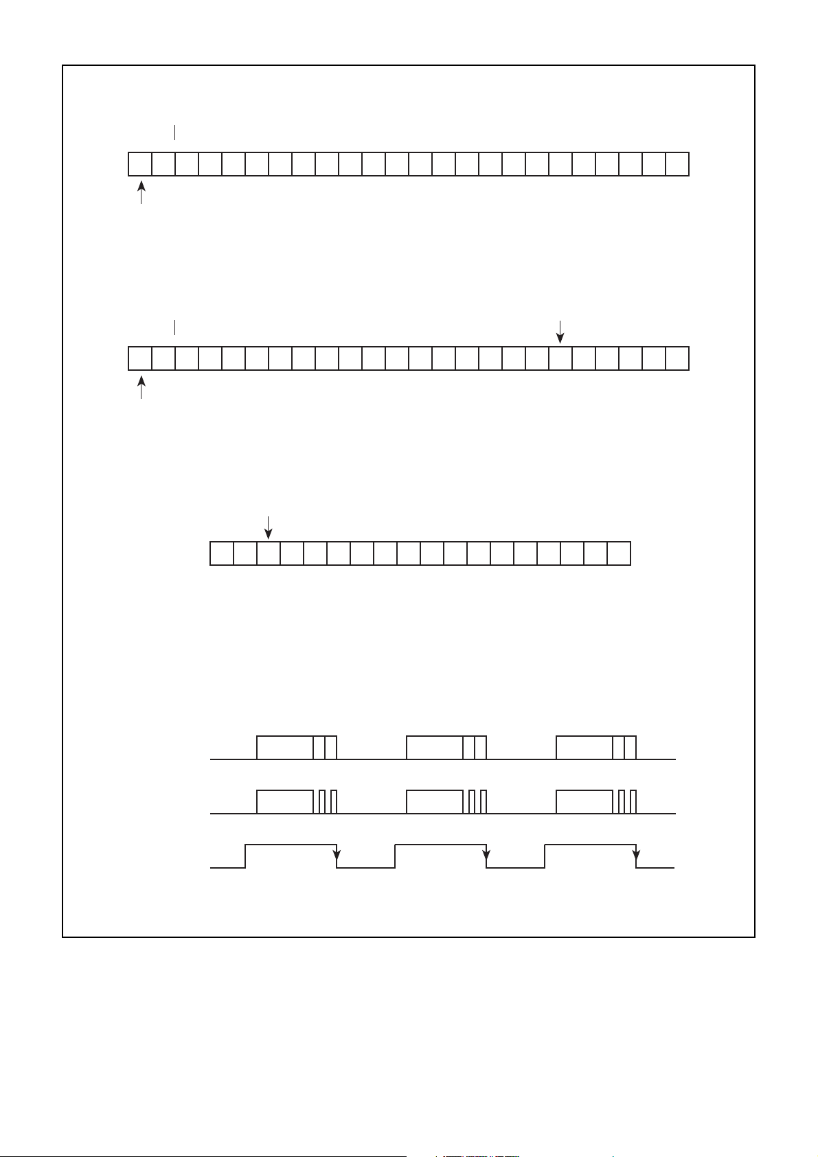
PHASE
DETECTOR GAIN
CONTROL
(SEE TABLE 3)
MSB LSB
G2 G1 21821721621521421321221121029282726252423222120C2 C1
PHASE
DETECTOR
SENSE BIT
15-BIT PROGRAMMABLE COUNTER (M COUNTER) 4-BIT
PROGRAMMABLE
COUNTER
(A COUNTER)
CONTROL
TABLE 3)
Fig. 6a F1 or F2 word, bit allocation with 416/17 selected
PHASE
DETECTOR GAIN
CONTROL
(SEE TABLE 3)
MSB LSB
G2 G1 2172162152142132122112102928272625242
PHASE
DETECTOR
SENSE BIT
15-BIT PROGRAMMABLE COUNTER (M COUNTER) 3-BIT
MUST BE ZERO
3
222120C2 C1
0
PROGRAMMABLE
COUNTER
(A COUNTER)
CONTROL
TABLE 3)
Fig. 6b F1 or F2 word, bit allocation with 48/9 selected
LOGIC
(SEE
LOGIC
(SEE
SP8858
DATA
CLOCK
ENABLE
DUAL MODULUS
N RATIO SELECT
0 = 416/17
1 = 48/9
MSB LSB
PD1 PD2 21221121029282726252423222120C2C
PHASE
DETECTOR
BISTABLE
CONTROL
(SEE TABLE 4)
13-BIT PROGRAMMABLE COUNTER (R COUNTER)
CONTROL
LOGIC
TABLE 3)
Fig. 6c Reference word bit allocation
F1 WORD F2 WORD REF WORD
22 BITS 0 0 22 BITS 1 0 16 BITS 1 1
22 CLOCKS
22 CLOCKS 16 CLOCKS
1
(SEE
DATA LOADS ON FALLING EDGES
Fig. 6d Data load sequence
Fig. 6 Data formats
7
Page 8
SP8858
controlling the dividers without disrupting the loop (and vice
versa). This facility can be used to reduce synthesiser switching
time by preparing the non-active buffer prior to the instant of
switching and can also be used to modify the open loop gain.
To ensure reliable data is loaded into the dividers the
internal control circuits ensure that the buffer data can only be
updated if the remaining M count is greater than 3. Given this
restriction, the maximum time taken to update the buffer after
the negative going ENABLE transition (or after F1/F2 has
been toggled) is:
[(31M) N1A]/RF input150ns
where update time is in seconds and RF input is in Hz.
The time taken to re-program the shift register (F1or F2)
is determined by the clock rate and the number of bits required
and is equal to:
243t
REP1tS1tE
If the reference buffer is selected (C2 = 1, C1 = 1), only the 16
LSBs of the shift register are used. 13 bits provide the data for the
Reference divider. Two bits, PD1 and PD2, control the charge
pump and the divider output buffer as shown in Table 4.
PD2 PD1 Result
0
0
1
1
F
0
1
0
1
and FPD outputs off, charge pump on
REF
and FPD outputs on, charge pump on
F
REF
and FPD outputs on, charge pump off
F
REF
F
and FPD outputs on, charge pump
REF
disabled by lock detect
The remaining bit of the Reference word is used to select
the prescaler modulus. A ‘1’ in this position selects the 8/9
mode. Note that when the 8/9 mode is selected the A divider
only requires 3 bits; the 4th bit must be set to ‘0’.
To ensure reliable data is loaded into the dividers the
internal control circuits ensure that the buffer data can only be
updated if the remaining R count is greater than 1. Given this
restriction, the maximum time taken to update the buffer after
the negative going ENABLE transition (or after F1/F2 has
been toggled) is:
1/F
Only 16 bits are required to program the reference buffer,
therefore reference programming time t
t
=163t
REF
If the Active A mode is programmed (C2=0. C1=1) only the
four A divider bits are updated at the end of the M count. The
M divider data, multiplication factor and phase detector sense
remain unchanged. This can be used to frequency hop to an
adjacent channel with the programming time reduced to:
Programming time (Active A) = 63t
The programming details discussed above are summarised
in Fig. 6.
Lock Detect
A simple Exclusive-OR phase detector together with an
integrator and comparator are used to indicate phase lock.
Capacitor CD on pin 28 sets the integrator time constant
and hence the sensitivity of the lock detect function. The
comparator controls a current sink connected to pin 27 which
can be used together with an external LED or resistor to
indicate phase lock.
The lock detect can also be used to disable the charge pump
by programming PD1 and PD2 of the reference word (Table 4).
(see Fig. 4)
Table 4
150ns
REF
REP1tS1tE
is:
REF
(see fig. 4)
REP1tS1tE
APPLICATIONS
Introduction
This section provides the basic information required to
implement a complete digital PLL synthesiser based on the
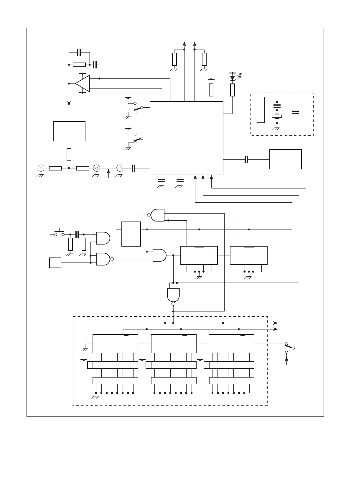
SP8858. A typical circuit is shown in Fig. 12 and is available
on a demonstration PCB, including a serial programmer. The
demonstration board can be used to evaluate the SP8858 and
can be readily adapted by the system/RF designer for a
specific application to aid in rapid prototype development.
Users of the SP8853 should consult Appendix A for details
of the design changes that are required to replace the SP8853
with the SP8858.
PLL Basics
A system level specification for a stable radio signal will
include measures of signal stability such as a single sideband
phase noise specification and a spurious output specification.
The power spectrum of the composite RF output signal is
influenced by a number of factors:
● Residual phase noise of the dividers
● Active loop filter residual noise
● Feedback divider ratio
● Phase detector gain
● VCO signal phase noise and gain
● Reference signal phase noise
● The closed loop root locations (an under damped loop will
cause a noise peak)
● Environmental influences such as EMI and power supply
noise
A single-loop synthesiser based around the SP8858 is
suitable for the synthesis of highly stable, low phase noise
signals provided each of the points above are carefully
considered.
The block diagram of a simple PLL is shown in Fig. 7.
PHASE
DETECTOR
(mA/RAD) K
F
(Hz)
REF
(s)
fi
FPD (Hz)
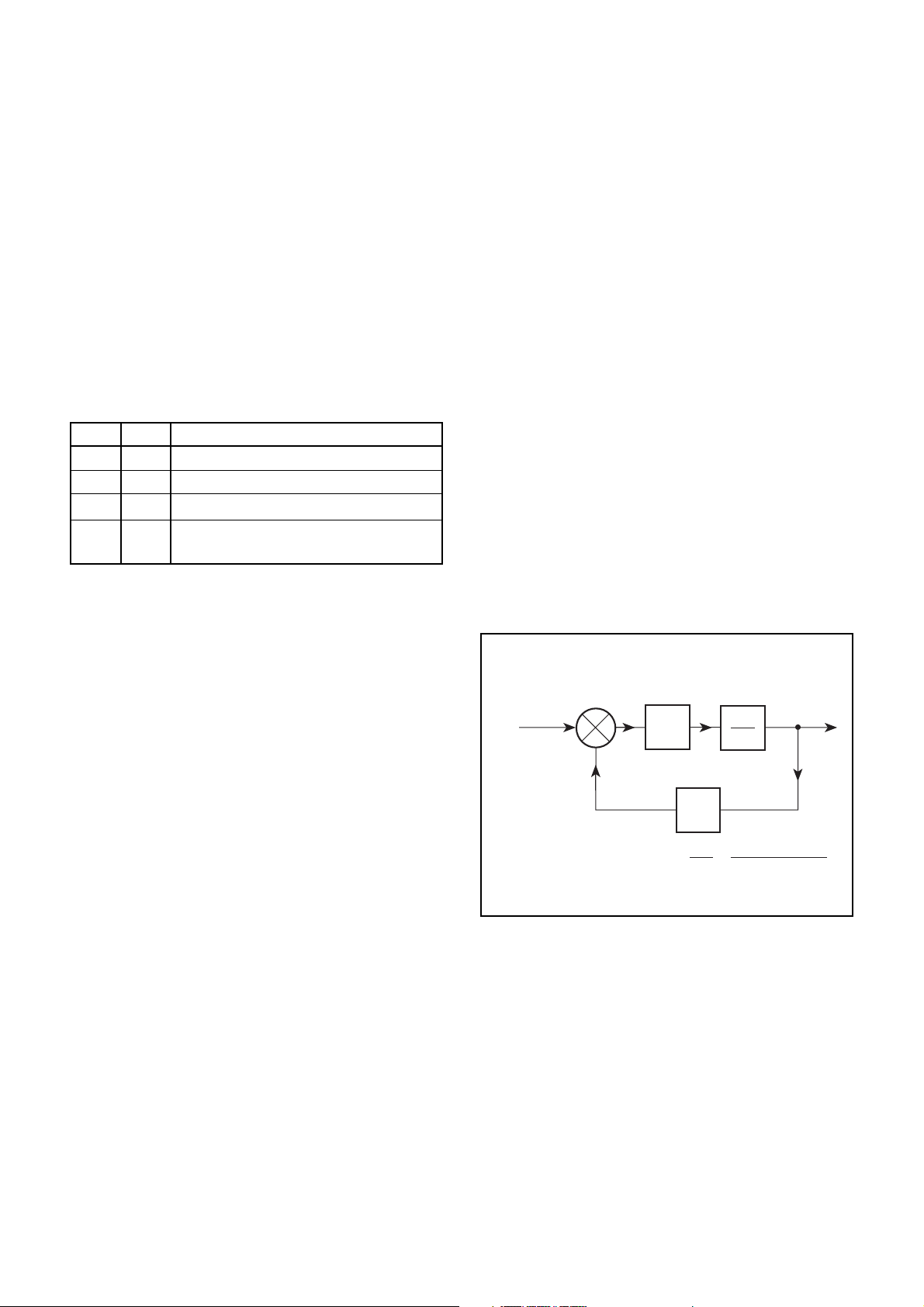
CLOSED LOOP RESPONSE =
OPEN LOOP DC GAIN =
The basic aim is to phase-lock the VCO signal to a stable
reference signal,
closed loop bandwidth and a high DC loop gain
(KPD3K
/N). This combination will ensure that the free-
VCO
running VCO phase noise is attenuated and that both the
long-term and the short-term stability of the output signal is
determined by the properties of the reference signal. A wide
loop bandwidth would also be consistent with the requirement
of many synthesiser specifications to change frequency and
regain phase lock within a specified time limit. In practice, the
following considerations limit the closed loop bandwidth and
the DC gain and, consequently, limit the extent to which the
ideal system is achieved:
LOOP FILTER
PD
(V/mA)
F(s)
DIVIDER
4
N
(s)
fo
f
(s)
i
K
VCO3KPD
VCO
(RAD/SEC/V)
K
VCO
s
F(s)3K
=
s1F(s)3K
/N
F
(Hz) fo(s)
O
VCO3KPD
VCO3KPD
/N
Fig. 7
fi(s) and, ideally, set a relatively wide
8
Page 9
● The divider in the feedback path imposes limitations on the
designer because it reduces the DC gain of the loop and
also because it unavoidably introduces a measurement
error. The contribution to
fo(s) phase noise power of the
fi(s) signal, at frequency offsets within the loop bandwidth,
is multiplied by N2 (i.e. increases by 20logN dB); this may
impose a specific loop bandwidth for optimum phase
noise.
● Physical imperfections in the charge pump and active loop
filter circuits force periodic corrections (at the rate of
1/F
) when the loop is phase-locked. The resulting
REF
disturbance frequency modulates the VCO producing
reference sidebands in the output signal spectrum. The
closed-loop bandwidth must be much less than F
REF
for
reasonable sideband suppression.
The design of the filter F(s), suitable for any given
application, may require careful trade-offs between the
requirement to meet the phase noise and the spurious output
specification and the settling time specification:
Example 1 In applications where high resolution is required
(the resolution is F
(less than F
REF
Hz) the imposed closed loop bandwidth
REF
Hz) could result in an unacceptably long time
to acquire phase lock.
Example 2 If a relatively high feedback division ratio is
required the 20logN increase in reference phase noise power,
seen at the output, could also impose a relatively narrow
closed loop bandwidth and hence a long acquisition time.
The roots of the characteristic equation in the closed loop
transfer function,
fo(s)/fi(s), are manipulated through
changes to the DC loop gain and the selection of the pole(s)
and zero(s) in F(s). Careful mathematical analysis is a
prerequisite to successful PLL synthesiser design. If the
analysis shows that the simple PLL as shown in Fig.12 is not
suitable then there are numerous modifications that can be
made to the basic loop and the texts listed in the References
should be consulted for more information.
The Mitel Application Note AN194 (Ref. 9) provides specific
guidance on noise minimisation and loop filter design for the
SP8858 user. The section Loop Filter Design below gives
details of the formula that can be used to implement the loopfilter given that the desired second order characteristics are
known, i.e. the desired natural loop frequency
v
and damping
n
factor z.
DESIGN IMPLEMENTATION
RF inputs
The availability of a suitable VCO should be considered
early in a project because information on the tuning range, the
tuning gain in Hz/V and the output noise spectrum is required
for the initial mathematical analysis. Variation in the tuning
gain over the tuning range should be minimised as this
parameter feeds into the closed loop characteristic equation.
There is also a trade-off between the requirement for a high
tuning gain (which requires the use of a relatively low Q
resonator) and phase noise.
The VCO, whether bought in or designed for the application,
must also be able to simultaneously drive the SP8858 RF input
as well as the input of the next stage in the system. A power
splitter and active buffer may be required in some applications.
The example in Fig.12 includes a simple resistive power
splitter. This type of buffer introduces a 6dB loss but is
adequate if the VCO output power is sufficient and if the
intention is simply to assess the SP8858 by monitoring the
output signal using a 50Ω measurement system.
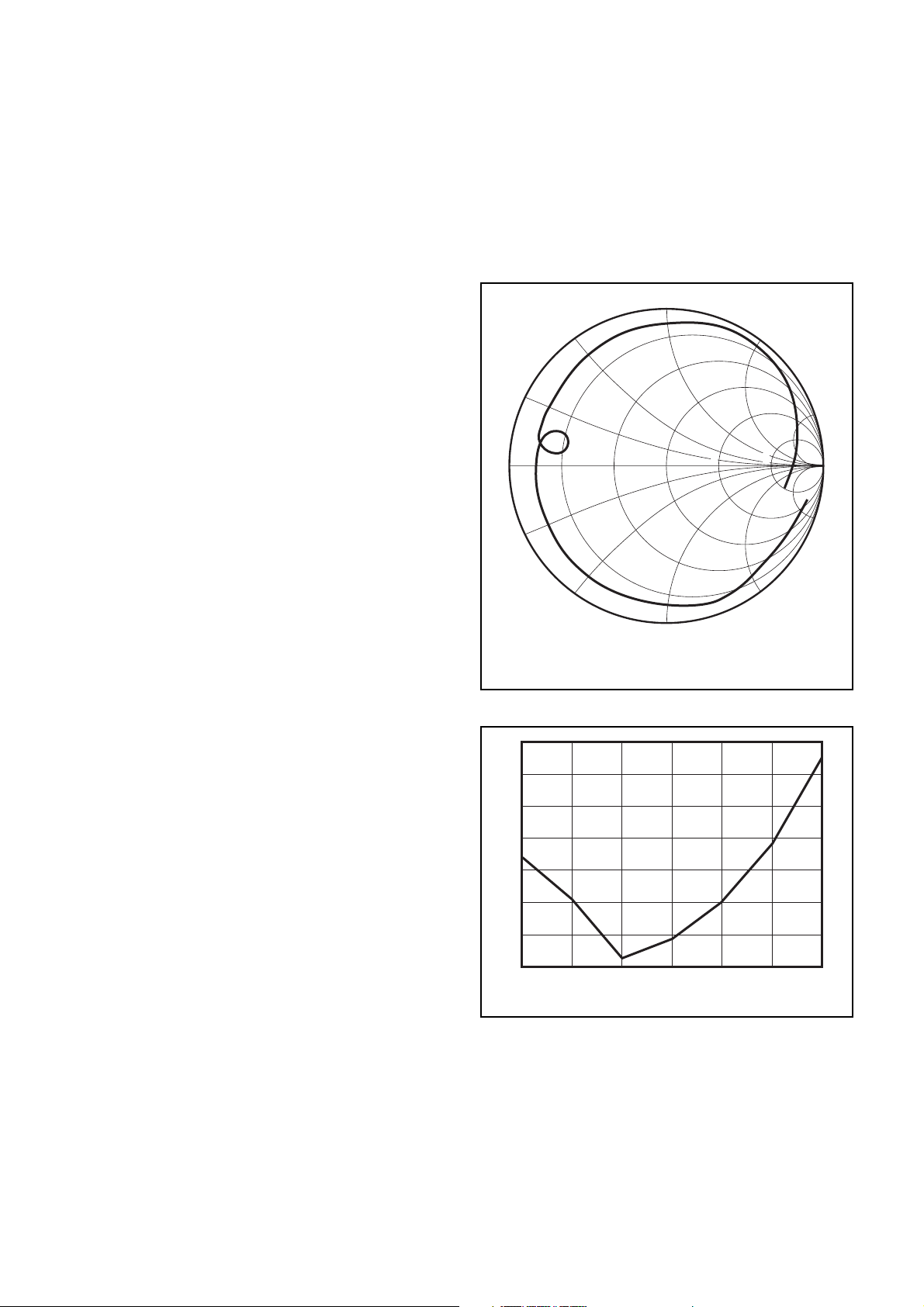
The SP8858’s RF input frequency specification covers the
range 80MHz to 1·5GHz and the input impedance varies with
frequency; a typical Smith chart is shown in Fig. 8. It is
advisable to consider transmission line effects for each
SP8858
individual application and to ensure that the minimum voltage
swing at the RF input is within the guaranteed operating range
over the full tuning range of the application. The SP8858
incorporates a pre-amplifier at the RF input and the dividers
can be seen to operate well below the guaranteed operating
range. Fig. 9 shows a typical sensitivity curve as measured on
the demonstration board board driven by a 50Ω signal
generator (sensitivity is the lowest power level at which the
divider operates without mis-counting). The dividers could be
more susceptible to spurious interference at low drive levels
causing the dividers to mis-count. However, driving the RF
input with relatively high levels will ensure greater immunity
from interference signals.
j
1
j
0.5
j
0.2
0.2
0
2
j
0.2
2
0.5
j
0.5
NORMALISED TO 50Ω
START 102MHz, STOP 2000MHz
1
j
2
2
1
Fig. 8 Demonstration board input impedance
0
25
210
215
220
225
230
235
50 100 500 1000 1500 2000 2300
RF INPUT FREQUENCY (MHz)
Fig. 9 Typical sensitivity for demo. board at 25°C
Reference Input
When the loop is phase-locked the output signal, Qo(s),
takes on the long term stability characteristics of the reference
signal. In many applications a crystal stabilised oscillator is
adequate as the reference source Qi(s). The VCO output
signal is divided down and compared with the reference
j
2
j
5
5
2
j
5
j
2
2
9
Page 10

SP8858
signal at the phase detector input. The multiplied reference
signal phase noise can set the limit on the achievable closein phase noise. It is important then that the reference signal is
a low phase noise source with good long term stability.
The residual noise of the reference divider is also important
because, at some offsets from the carrier, the dividers limit the
phase noise reduction that is achievable when the reference
signal is divided down to F
noise optimisation is given in Ref. 1.
Charge Pump Output
CP OUTPUT (pin 26) and CP REF (pin 5) are connected
directly to the inverting and non-inverting input of the loop filter
amplifier respectively as shown in Fig. 12. The CP OUTPUT
pin will source/sink a current to/from the inverting input equal
in magnitude to, or a multiple of, a current reference flowing
into RPD (pin 24). The multiplication factor is programmed by
two bits (G1 and G2) in the F1 or F2 word (see Data Entry and
Control section).
The CP OUTPUT has two stable states. The ON state
sourcing or sinking a fixed current and an OFF state in which
no current will flow from or into the CP output pin. The
proportion of time the charge pump is ON depends on the
frequency/phase relationship between the reference signal
(divided by R) and the VCO signal (divided by N) at the phase
detector input:
● The digital phase detector is sensitive to a frequency
difference between the two input signals and will source or
sink a constant current for frequency differences.
● When phase-lock is acquired the charge pump current ON/
OFF ratio is in direct proportion to the phase difference
between the two signals at the phase detector input.
Starting from the state ‘charge pump OFF’ the edge of the
leading signal triggers the charge pump into the ON state.
The edge of the lagging signal briefly triggers a current at
the output which is opposite in sign and equal in magnitude
to the current already present before the charge pump
returns to the OFF state. When the phase difference
reaches zero the input signals simultaneously trigger brief
source and sink current pulses which cancel at the output
so that zero phase error gives zero output and the deadband
is eliminated. The pulse widths are determined by the time
taken to reset the internal flip-flops.
In practice, when the loop is phase locked and the charge
pump is predominately in the OFF state there are two
imperfections to consider:
● The loop filter capacitors discharge during the period of the
reference signal.
● A small current leaks into CP OUTPUT in the OFF state at
high charge-pump current settings.
A small correction is therefore required each cycle. The
resulting disturbance is attenuated by the loop but any residual
ripple on the VCO control frequency modulates the VCO
causing the characteristic reference sidebands. The magnitude
of the sidebands that can be tolerated depends entirely on the
application and can be reduced by setting a loop bandwidth
very much less than the phase detector comparison frequency
(F
) or by reducing the charge-pump current (the leakage
REF
current is negligible for low charge-pump currents).
The charge-pump can be set to source or sink a current for
any given phase difference and the SENSE bit in the F1 (or
F2) programme word is used to set the appropriate sign for the
application. The SENSE bit should be set to 1 for a VCO with
a positive frequency versus control voltage characteristic to
ensure phase lock.
The actual bias voltage at the CP REF pin varies with the
magnitude of the reference current and CP OUT is held at the
same voltage by the operational amplifier. A low offset voltage
. More detailed advice on phase
REF
amplifier should be chosen to maintain the match between the
reference current into RPD (pin 24) and the actual output
current.
The simplest method of setting the reference current is to
connect a resistor between RPD and the supply. The voltage
at pin 24 is approximately 1·5V but this varies slightly with the
magnitude of the current and a simple calculation of Ipin 24 =
(V
21·5)/RPD (see Description, Data Entry and Control) is
CC
approximate. The voltage at pin 24 will also vary with
temperature and the impact of the phase detector gain
variations on performance should be assessed in each
individual application. If it is considered important to improve
the accuracy of the phase detector gain then the use of a
constant current source may be more appropriate.
Miscellaneous I/Os
The SP8858 includes simple lock-detect circuit. The output
signals from the Reference and RF dividers are used to drive
an EXOR type phase detector. The output of this type of
detector is logic high if the inputs are at the same voltage level
and low if the inputs are polarised. The EXOR gate drives a
buffer stage with the output collector loaded with a single
50kΩ on-chip resistor and a capacitor connected externally at
pin 28 (CD). The RC serves to integrate the output pulse train
from the phase detector. The capacitor voltage must reach a
fixed threshold to enable a constant current sink into pin 27.
The inputs POWER DOWN and F1/F2 can either be fixed
at the required logic level or controlled by some peripheral
circuit. See Table 1 and Fig. 12.
As with any RF design work care must be taken with the
power supply layout to and the returns from the IC and the
physical position of the PLL on the PCB in relation to potential
interference sources. The V
supply inputs should be
CC
connected to a well regulated 5V power supply and locally
decoupled; noise on the supply can influence the noise power
spectrum of the output signal.
The programming inputs DATA, CLOCK and ENABLE are
compatible with standard CMOS and TTL logic and are
subject to the timing restrictions shown in Fig. 4.
Loop Filter Design
The linear model of the PLL, as shown in Fig.7, includes an
external loop-filter F(s). A filter is required that will:
● Add a zero to the open-loop transfer function thus allowing
the designer to manipulate the closed-loop root locations
through the appropriate choice of filter components. Without
the filter (F(s) = 1) the closed loop is first order with the root
locus travelling along the negative real axis with increasing
DC gain. In this situation the designer has very little control
over the
selection of the gain factor KPD K
limited.
● Introduce a second pole at the origin in order to increase
the type number of the loop to type II. This is required to
ensure that the steady state error signal tends to zero for
a ramp in phase.
In addition, a suitable interface is required to provide the
transimpedance function from the charge-pump output to the
VCO thus converting the output signal, in the form of current
pulses, to the voltage signal required at the VCO input.
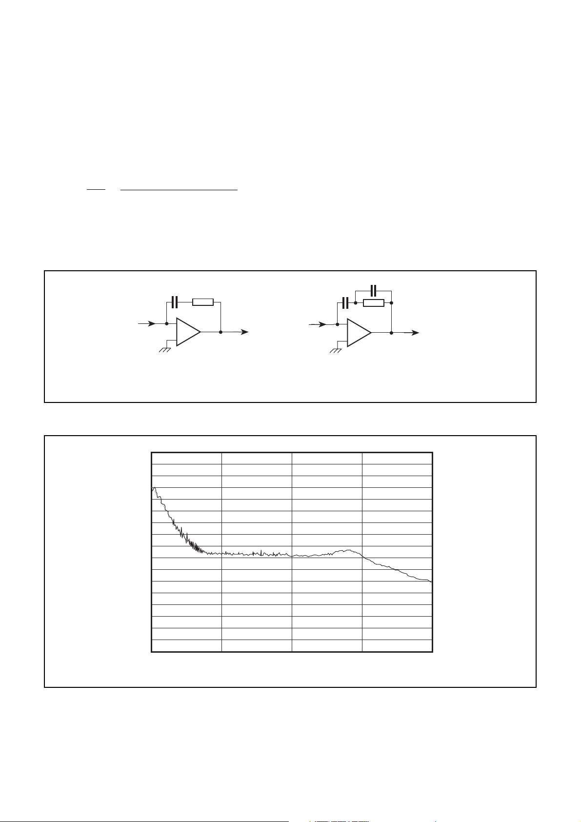
The required transfer function is therefore F(s) = (s+a)/s
(zero at 2a) and the loop filter is implemented using the circuit
and formula shown in Fig. 10a. The closed-loop transfer
function becomes:
fo(s)/fi(s) = (st
where K = K
fo(s)/fi(s) transfer characteristic because the
/N may, in practice, be
VCO
11)K
1
t
= C1R1
1
VCOKPD
/(s21st1K/C11K/C1)
VCOKPD
/N
10
Page 11
The selection of C1 and R1 is often approached by using
the standard representation for the second order characteristic
equation: s
2
12zv
2
and selecting the natural-loop
n1vn
frequency and the damping factor z to give the desired
response. The time constants are calculated using:
2
zv
n = t1
C1 = K/
K/C1 and v
2
v
and R1 = 2zvn/K
n
2
= K/C1 so that
n
Alternatively, the loop filter and formula shown in Fig. 10b
can be used to introduce a pole in F(s) at 21/t2 which will
provide additional roll-off in the closed loop transfer
characteristic in order to attenuate the reference sidebands.
The closed loop transfer function becomes:
fo(s)
fi(s)
[s(
t
)11]K
=
[C1t2s31C1s21K(t11t2)s1K]
11t2
VCOKPD
Care must be taken when choosing C2 to ensure that the
additional pole does not unduly affect the stability margins of
the loop. In practice, a simple and useful rule of thumb is to set
the desired second order response as above and then set C2
to be 1/10 of C1. It is advisable when designing third order or
C1
R1
SP8858
higher order loops to use CAD tools to assess stability.
Popular analysis tools taken from control theory, such as root
locus and Bode diagrams, are useful to aid the design of the
closed loop PLL system. AN194 describes these tools in more
detail and introduces a loop filter design methodolgy aimed at
optimising the phase noise performance.
Loop filter design example
Use the demonstration board to generate a 1GHz signal
with a resolution of 500kHz (N = 5000) and reference oscillator
frequency of 40MHz. Set natural loop frequency,
4
2
p310
rad/s and damping factor to 0·7. The MQE001-1016
VCO gain, K
output current to 2mA so that K
, is nominally 25MHz/V. Set the phase detector
VCO
= 231023/2p A/rad.
PD
Using the above formula, calculate the loop filter R and Cs.
K = 2
p325310
C1 = 10/(2
R1 = 230·732p3104/10 ≈ 8796
C2 = C1/10 ≈ 0·25310
6
3231023/2p35000 = 10
4
p310
)32 ≈ 2·5310
29
29
Realise the loop filter with C1 = 2·2nF, C2 = 220pF and
R1 = 8·2kΩ. The single sideband phase noise specturm for
this example is shown in Fig. 11.
C2
C1
v
, to
n
Ii(s)
−
+
Vo (s) /Ii(s) = [s(t111]/sC1
where t1 = C1R1
Fig. 10a
I
(s)
i
V
(s)
o
Vo (s) /Ii(s) = [s(t11t2)11]/sC1(st211)
t
1 = C1R1 and t2 = C2R1
where
R1
−
+
Fig. 10b
Fig. 10 Loop filters
0
210
220
230
240
250
260
270
280
290
2100
2110
2120
2130
NOISE AMPLITUDE (dBc/Hz)
2140
2150
2160
2170
10Hz 100Hz 1kHz 10kHz 100kHz
FREQUENCY
(s)
V
o
Fig. 11
11
Page 12
SP8858
C4
F
REFFPD
C6
R1
1V
OP
−
OP27
+
2V
OP
CONTROL
MURATA
MQE001-1016
VCO
R7
SMA SMA
NOTES
1. PINS 1, 3, 17 AND 21 ARE NC
2. PINS 2, 7, 11, 12, 19, AND 22 = GND
3. PINS 8, 9, 18 AND 23 = 15V
4. DECOUPLING CAPACITORS NOT SHOWN
SEND
15V
OSC
C14
R4 R3
1MHz CLK
R5R6
LINK TO
COMPLETE
PLL
1
HC08
2
1
HC00
2
POWER
DOWN
F1/F2
RF INPUT
SMA
LOGIC ‘1’
2
3
3
3
15V
15V
C43
1
CLR
D
Q
HC74
CLK
PRE
4
LOGIC ‘1’
R12 R13
15V
15V
26 25 5 4 24
6
13
10
C40
SP8858
11 28 16 15 14
C32
R2
27
20
R10
Alternative reference oscillator
100n
(INADVERTENTLY
LABELED R9
ON BOARD)
21
20
33p
10MHz
40MHz
REFERENCE
OSCILLATOR
33p
DATA
CLOCK
ENABLE
HC20
HC08
5
4
2
1
711
LOADQ
D
512
6
HC193a
UP CO
ABCD
15 1 10 9
311
LOADQ
A
5
HC193b
UP
ABCD
15 1 10 9
6
5
4
5
12
21
CLK SH/LD
10 9
SER
HC165c
A B C D E F G H
12 13 14 3 4 5 6
11
15V
SILc
SWITCHc SWITCHb SWITCHa
910
HC00
8
21
CLK SH/LD
10 9
Q
H
SER
A B C D E F G H
11 12 13 14 3 4 5 6
15V
HC165b
10 9
Q
H
SER
A B C D E F G H
11
15V
SILb
CIRCUIT IN DOTTED LINES IS DUPLICATED
Fig. 12 SP8858 demonstration board
21
CLK SH/LD
HC165a
12 13 14 3 4 5 6
Q
SILa
TO SHIFT
REGISTER
d, e AND f
H
FROM SECOND
PROGRAMMABLE
SHIFT REGISTER
d, e AND f
Page 13
SP8858
Integrated circuits
SP8858 1·5GHz synthesiser
OP27 Operational amplifier
HC00
HC08
HC20
HC74
HC165 (6 off)
HC193 (2 off)
Leaded resistors and capacitors
R1, C4 and C6: Application specific to define the loop filter
characteristic (no components fitted)
R2: 6·8kΩ
C1, C2, C7 and C10: 10µF Tantalum
C3, C5, C8 and C9: 0·1µF Ceramic
Chip resistors (0805)
R3, R12, and R13: 3·3kΩ
R4:10kΩ
R5, R6 and R7: 15Ω
R8: 100Ω
R10: 2·2kΩ
R11: No component
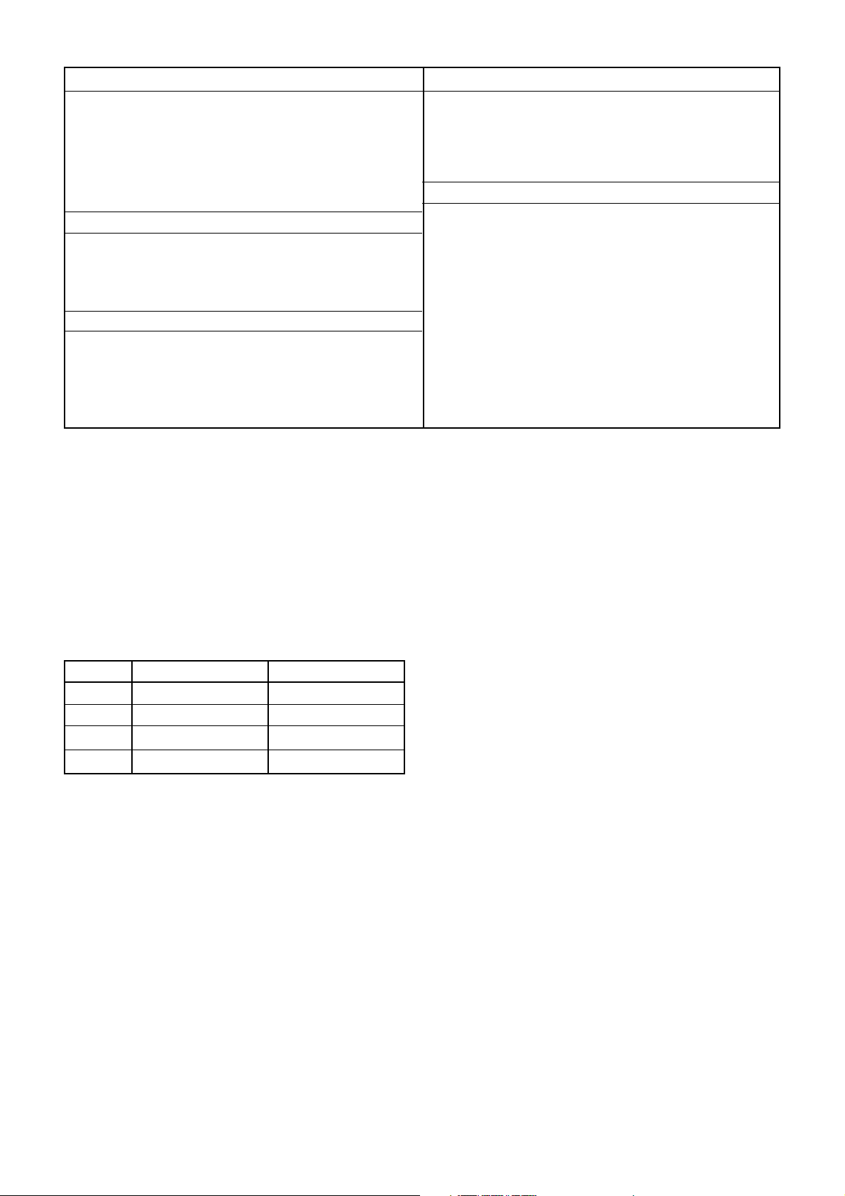
Table 5. Demonstration board parts list
APPENDIX A: SP8853 TO SP8858
The SP8858 is not a drop-in replacement for the SP8853;
minor modifications will be required to a SP8853-based
design if the SP8858 is to be used in its place. The changes
mainly affect the charge pump output pins as shown in Table
6 below. The SP8858 has only one charge pump output.
In addition the modifications have:
● Increased the operating frequency range for both the RF
and reference input
● Simplified the lock detect circuit
● Increased the maximum charge-pump current specification
to 2mA. Recalculate the loop filter components using
formula in Application section.
PIn No.
1
3
25
26
SP8853
Internally connected
PD1 output
PD2 output
NC
Table 6
SP8858
NC
NC
CP OUTPUT
CP REF
Chip capacitors (0805)
C11 through C26, C28, C29, C33, C34, C36 through C39,
C41 and C42: 0·1µF
C14: 1nF
C32: 220pF
C40 and C43: 100pF
C27, C30, C31 and C35: No components
Miscellaneous
Murata MQE001-106 VCO
40MHz crystal oscillator
1MHz clock oscillator for programmer logic
PCB keyboard switch (SEND)
Slide switches (3 off) (SELECT, F1/F2, POWER DOWN)
16-pin DIL switch (6 off) (SIL a, b, c, d, e and f)
SMA PCB mounting socket (3 off)
REFERENCES
1. Knights P.J.,
Synthesiser for Low Phase Noise
East 1994, Nov 1994.
2. Gardener F.M.,
3. Rohde U.L.,
Design
4. Manassewitsch V.,
Design
5. Philips C.L. and Harbur R.D.,
Prentice Hall 1991.
6. Scherer D.,
April 1979 p.116.
7. Robins W.P.,
Peregrineus Ltd. (IEE) 1991.
8. Breed G.A. (ed.),
Collection from RF Design,
1992.
9. AN194,
Noise
Analysis and Design of a SP8858 Digital PLL
, Proceeding of RF Expo
Phaselock Technique
, Wiley 1979.
Digital Frequency Synthesisers Theory and
, Prentice Hall 1983.
Frequency Synthesisers Theory and
,
Wiley 1980.
Feedback Control Systems
Learn About Low Noise Design,
Phase Noise in Signal Sources
Microwave
, Peter
Frequency Synthesis Handbook, A
Cardiff Publishing Co. May
The SP8858 Synthesiser: Design for Low Phase
, Mitel Semiconductor
,
13
Page 14
Page 15
Page 16
Page 17

http://www.mitelsemi.com
World Headquarters - Canada
Tel: +1 (613) 592 2122
Fax: +1 (613) 592 6909
North America Asia/Pacific Europe, Middle East,
Tel: +1 (770) 486 0194 Tel: +65 333 6193 and Africa (EMEA)
Fax: +1 (770) 631 8213 Fax: +65 333 6192 Tel: +44 (0) 1793 518528
Fax: +44 (0) 1793 518581
Information relating to products and services furnished herein by Mitel Corporation or its subsidiaries (collectively “Mitel”) is believed to be reliable. However, Mitel assumes no
liability for errors that may appear in this publication, or for liability otherwise arising from the application or use of any such information, product or service or for any infringement of
patents or other intellectual property rights owned by third parties which may result from such application or use. Neither the supply of such information or purchase of product or
service conveys any license, either express or implied, under patents or other intellectual property rights owned by Mitel or licensed from third parties by Mitel, whatsoever.
Purchasers of products are also hereby notified that the use of product in certain ways or in combination with Mitel, or non-Mitel furnished goods or services may infringe patents or
other intellectual property rights owned by Mitel.
This publication is issued to provide information only and (unless agreed by Mitel in writing) may not be used, applied or reproduced for any purpose nor form par t of any order or
contract nor to be regarded as a representation relating to the products or services concerned. The products, their specifications, services and other information appearing in this
publication are subject to change by Mitel without notice. No warranty or guarantee express or implied is made regarding the capability, performance or suitability of any product or
service. Information concerning possible methods of use is provided as a guide only and does not constitute any guarantee that such methods of use will be satisfactory in a specific
piece of equipment. It is the user’s responsibility to fully determine the performance and suitability of any equipment using such information and to ensure that any publication or
data used is up to date and has not been superseded. Manufacturing does not necessarily include testing of all functions or parameters. These products are not suitable for use in
any medical products whose failure to perform may result in significant injury or death to the user. All products and materials are sold and services provided subject to Mitel’s
conditions of sale which are available on request.
M Mitel (design) and ST-BUS are registered trademarks of MITEL Corporation
Mitel Semiconductor is an ISO 9001 Registered Company
Copyright 1999 MITEL Corporation
All Rights Reserved
Printed in CANADA
TECHNICAL DOCUMENTATION - NOT FOR RESALE
 Loading...