

Page 1
SP8720
ADVANCE INFORMATION
DS3650-1·2
300MHz
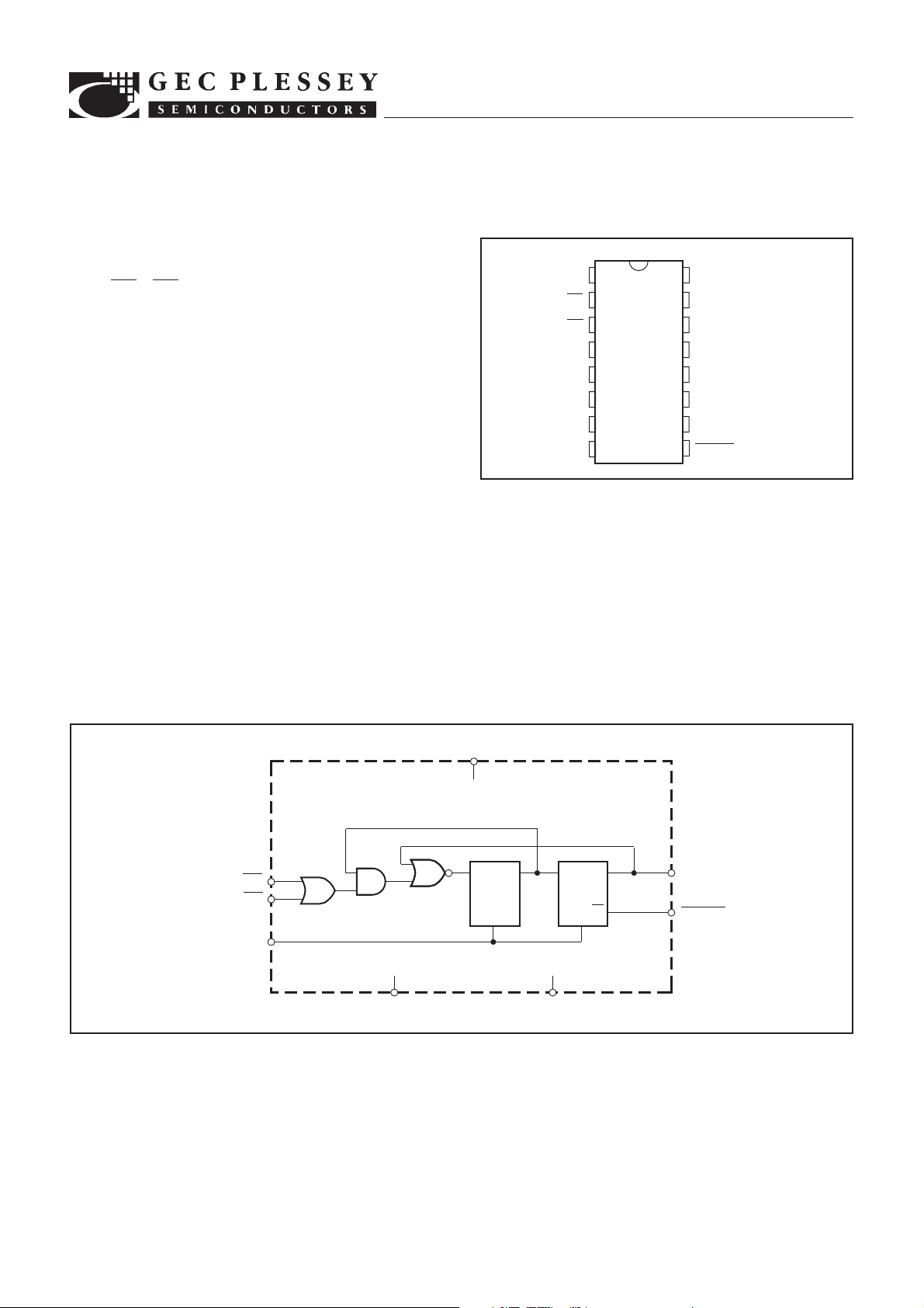
The SP8720 is an ECL two-modulus divider, with ECL10K
compatible outputs. It divides by 3 when either of the ECL control
inputs, PE1 or PE2, is in the high state and by 4 when both are low
(or open circuit). An AC coupled input of 600mVp-p is required.
FEATURES
■ ECL Compatible Outputs
■ AC-Coupled Input (Internal Bias)
■ Control Inputs ECL III/10K Compatible
QUICK REFERENCE DATA
■ Supply Voltage: 25·2V
■ Power Consumption: 240mW
■ Temperature Range:
255°C to 1125°C (A Grade)
230°C to 170°C (B Grade)
ABSOLUTE MAXIMUM RATINGS
Supply voltage
Output current
Storage temperature range
Max. junction temperature
Max. clock input voltage
265°C to 1150°C
28V
20mA
1175°C
2·5V p-p
44
43/4
44
PE1
PE2
NC
V
CC
NC
NC
1
2
3
4
5
6
7
8
SP8720
CLOCK INPUT
CONTROL
INPUTS
OUTPUT
Fig. 1 Pin connections - top view
ORDERING INFORMATION
SP8720 A DG
SP8720 B DG
5962-90577 (SMD)
16
INTERNAL BIAS DECOUPLING
15
NC
14
NC
13
NC
12
V
EE
11
DO NOT CONNECT
10
NC
9
OUTPUT
DG16
PE1
PE2
CLOCK INPUT
V
(0V)
CC
5
2
3
1
16
INTERNAL BIAS
DECOUPLING
D1CKQ1 D2CKQ2
Q2
12
V
EE
8
9
OUTPUT
OUTPUT
Fig. 2 Functional diagram
Page 2
SP8720
ELECTRICAL CHARACTERISTICS
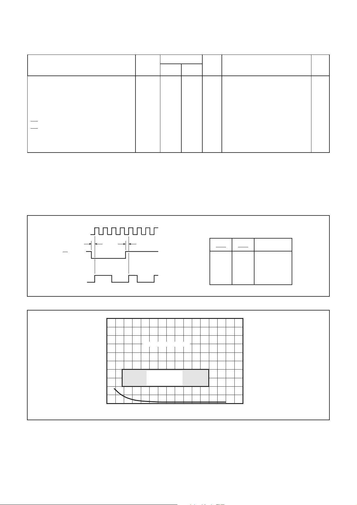
Unless otherwise stated, the Electrical Characteristics are guaranteed over specified supply, frequency and temperature range
Supply voltage, VCC = 0V, VEE = 25·2V 6 0·25V
Temperature, T
Characteristic
= 255°C to 1125°C (A Grade), 230°C to 170°C (B Grade)
AMB
Value
Symbol
Min.
Max.
Units
Conditions
Notes
Maximum frequency (sinewave input)
Minimum frequency (sinewave input)
Power supply current
Output high voltage
Output low voltage
PE input high voltage
PE input low voltage
Clock to output delay
Set-up time
Release time
NOTES
1. The temperature coefficients of V
2. The test configuration for dynamic testing is shown in Fig.6.
3. The set-up time t
to ensure that the 43 mode is obtained.
4. The release time t
to ensure that the 44 mode is obtained.
5. SP8720B tested at 25°C only.
6. Guaranteed but not tested.
is defined as the minimum time that can elapse between L→H transition of control input and the next L→H clock pulse transition
s
is defined as the minimum time that can elapse between H→L transition of control input and the next L→H clock pulse transition
r
CLOCK INPUT
PE INPUT
OUTPUT
= 11·63mV/°C, VOL = 10·94mV/°C and of VIN = 11·22mV/°C.
OH
t
r
2
2
f
MAX
f
MIN
I
EE
V
OH
V
OL
V
INH
V
INL
t
p
t
s
t
r
t
s
1
2
300
20·85
21·8
20·93
2·5
3
40
65
20·7
21·5
21·62
6
MHz
MHz
mA
V
V
V
V
ns
ns
ns
Input = 400-800mV p-p
Input = 400-800mV p-p
V
= 25·2V
EE
V
= 25·2V (25°C)
EE
V
= 25·2V (25°C)
EE
V
= 25·2V (25°C)
EE
V
= 25·2V (25°C)
EE
TRUTH TABLE FOR
CONTROL INPUTS
PE1
L
H
L
H
PE2 Division ratio
L
L
H
H
5
5
5
6
3, 6
4, 6
4
3
3
3
Fig. 3 Timing diagram
2000
1600
T
= 255°C TO 1125°C
(mV p-p)
1200
800
INPUT AMPLITUDE
400
0
0 100 200 300 400
AMB
GUARANTEED
OPERATING
WINDOW
INPUT FREQUENCY (MHz)
*
*
Tested as specified
in table of Electrical
Characteristics
Fig. 4 Typical input characteristic of SP8720A
2
Page 3
OPERATING NOTES
1. The clock input is biased internally and is coupled to the signal
source with a suitable capacitor. The input signal path is completed
by an input reference decoupling capacitor which is connected
from pin 16 to ground.
2. If no signal is present the device will self-oscillate. If this is
undesirable, it may be prevented by connecting a 15kΩ resistor
from the clock input (pin 1) to V
sensitivity by approximately 100mV.
3. The circuit will operate down to DC but slew rate must be better
. This will reduce the input
EE
j
0.5
j
0.2
SP8720
than 100V/µs.
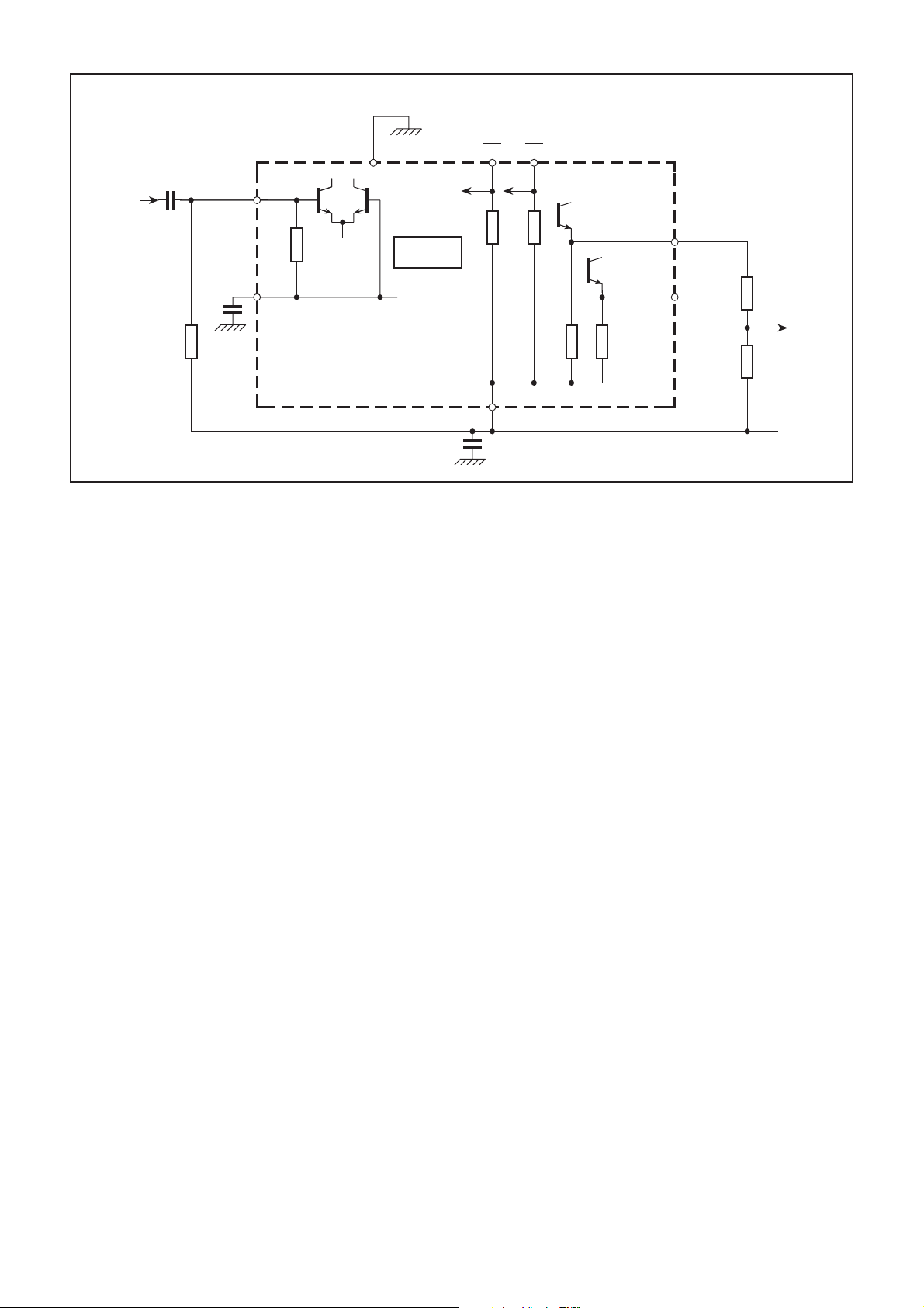
4. The Q and Q outputs are compatible with ECLII but can be
interfaced to ECL10K as shown in Fig. 7. There is an internal
circuit equivalent to a load of 2kΩ at each output.
5. The PE inputs are ECLIII/10K compatible and include 4·3kΩ
pulldown resistors. Unused inputs can therefore be left open.
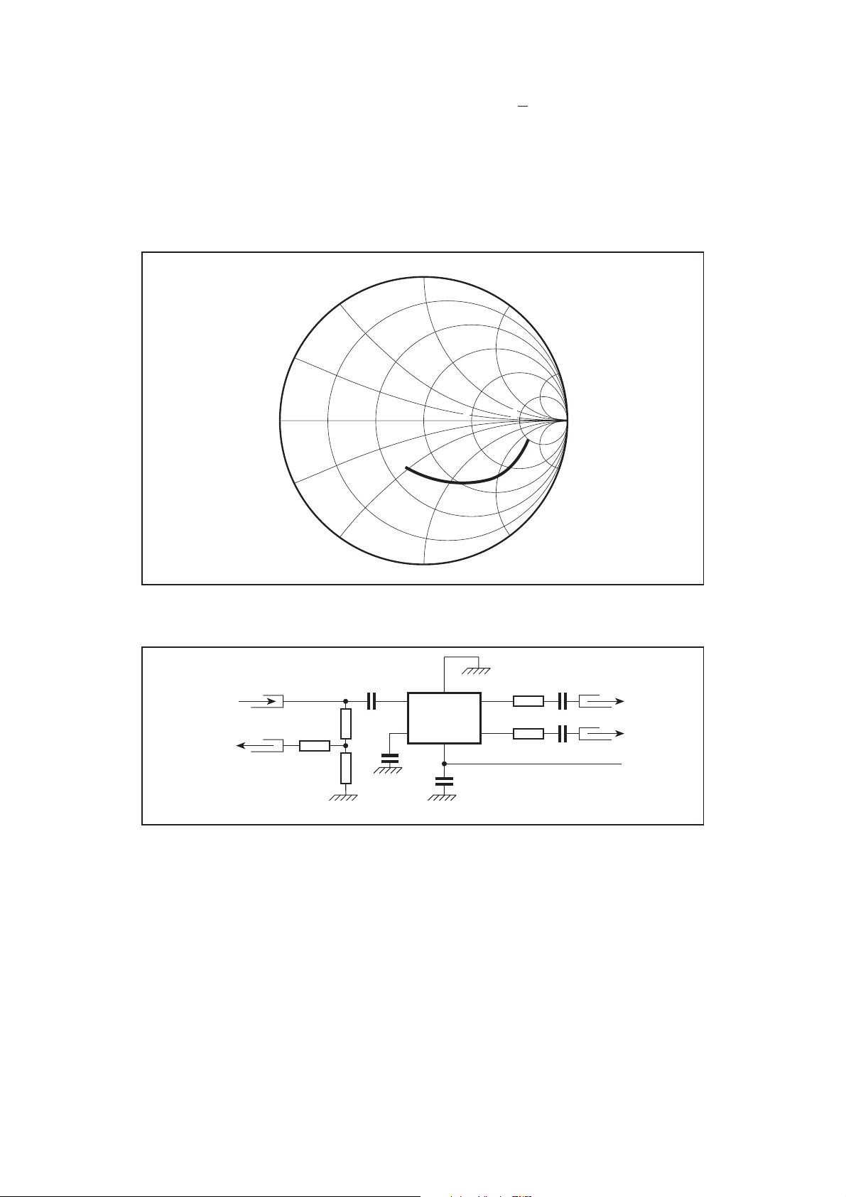
6. The input impedance of the SP8720 varies as a function of
frequency, see Fig. 5.
7. All components should be suitable for the frequency in use.
j
1
j
2
j
5
0.2
0
2
j
0.2
2
0.5
j
0.5
300
1
250
j
2
2
200
1
150
5
100
2
50
j
5
2
j
2
Fig. 5 Typical input impedance. Test conditions: Supply Voltage = 25·2V,
Ambient Temperature = 25°C. Frequencies in MHz, impedances normalised to 50Ω .
INPUT FROM
GENERATOR
TO SAMPLING
SCOPE
1n
1
33
33
16
20
1n
DUT
5
8
9
12
1n
450
450
100n
100n
OUTPUTS TO
SAMPLING
SCOPE
V
= 25·2V
EE
Fig. 6 Test circuit
3
Page 4
SP8720
CLOCK
INPUT
1n
ECL CONTROL INPUTS
0 = 4
1 = 3
PE1 PE2
5
1
400
DIVIDE BY
3/4
23
4·3k4·3k
8
15k
1n
16
BIAS
12
1n
Fig. 7 Typical application circuit showing interfacing
2k 2k
9
47
1·5k
ECL10K
OUTPUT
V
EE
4
Page 5

NOTES
SP8720
5
Page 6
SP8720
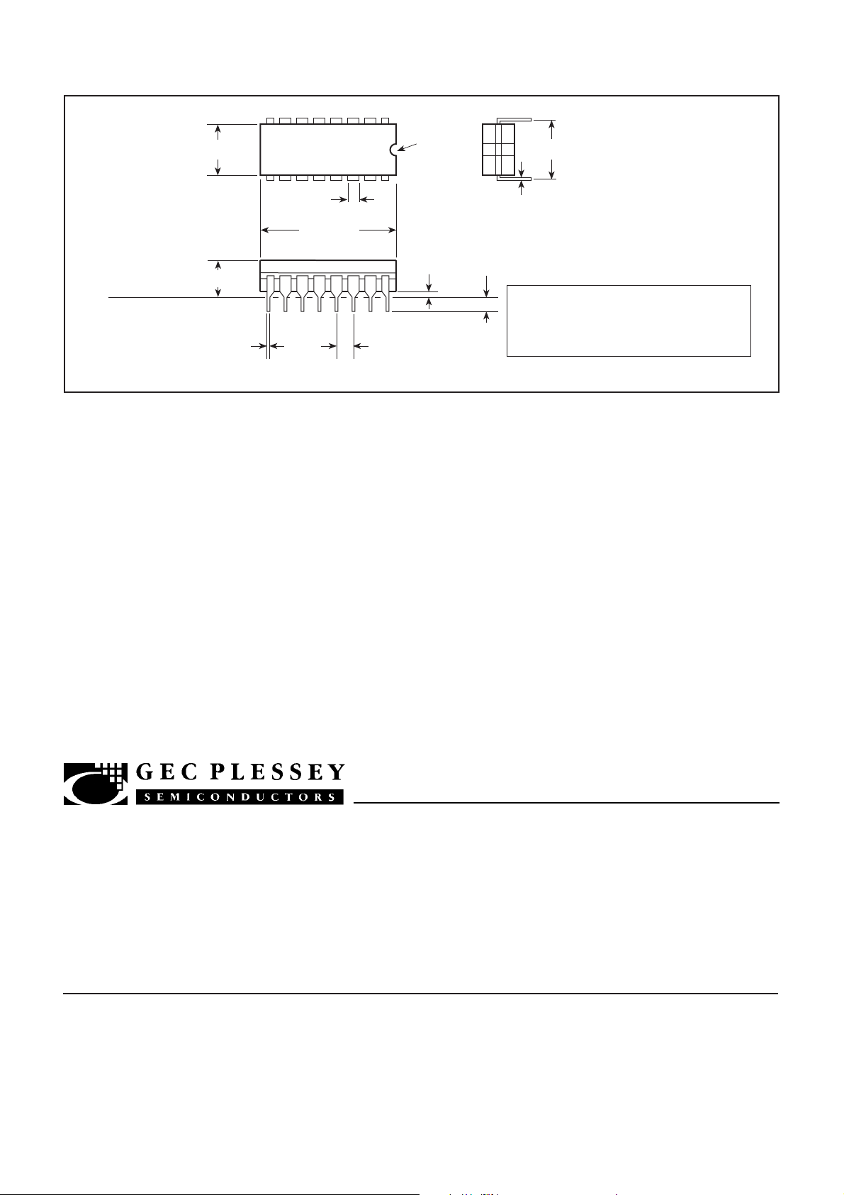
PACKAGE DETAILS
Dimensions are shown thus: mm (in).
1
SEATING PLANE
5·59/7·87
(0·220/0·310)
5·08/(0·20)
MAX
0·36/0·58
(0·014/0·23)
1·14/1·65
(0·045/0·065)
20·32 (0·800)
PIN 1 REF
NOTCH
MAX
16
0·51 (0·02)
MIN
(0·125/0·160)
(0·008/0·014)
3·18/4·06
0·20/0·36
NOTES
1. Controlling dimensions are inches.
2. This package outline diagram is for guidance
16 LEADS AT 2·54 (0·10)
NOM. SPACING
only. Please contact your GPS Customer
Service Centre for further information.
16-LEAD CERAMIC DIL – DG16
7·62 (0·3)
NOM CTRS
HEADQUARTERS OPERATIONS
GEC PLESSEY SEMICONDUCTORS
Cheney Manor, Swindon,
Wiltshire SN2 2QW, United Kingdom.
Tel: (0793) 518000
Fax: (0793) 518411
GEC PLESSEY SEMICONDUCTORS
P.O. Box 660017
1500 Green Hills Road,
Scotts Valley, CA95067-0017
United States of America.
Tel (408) 438 2900
Fax: (408) 438 5576
This publication is issued to provide information only which (unless agreed by the Company in writing) may not be used, applied or reproduced for any purpose nor form part of any order or contract nor to be regarded
as a representation relating to the products or services concerned. No warranty or guarantee express or implied is made regarding the capability, performance or suitability of any product or service. The Company
reserves the right to alter without prior knowledge the specification, design or price of any product or service. Information concerning possible methods of use is provided as a guide only and does not constitute
any guarantee that such methods of use will be satisfactory in a specific piece of equipment. It is the user's responsibility to fully determine the performance and suitability of any equipment using such information
and to ensure that any publication or data used is up to date and has not been superseded. These products are not suitable for use in any medical products whose failure to perform may result in significant injury
or death to the user. All products and materials are sold and services provided subject to the Company's conditions of sale, which are available on request.
CUSTOMER SERVICE CENTRES
●
FRANCE & BENELUX Les Ulis Cedex Tel: (1) 64 46 23 45 Fax : (1) 64 46 06 07
●
GERMANY Munich Tel: (089) 3609 06-0 Fax : (089) 3609 06-55
●
ITALY Milan Tel: (02) 66040867 Fax: (02) 66040993
●
JAPAN Tokyo Tel: (3) 5276-5501 Fax: (3) 5276-5510
●
NORTH AMERICA Scotts Valley, USA Tel: (408) 438 2900 Fax: (408) 438 7023.
●
SOUTH EAST ASIA Singapore Tel: (65) 3827708 Fax: (65) 3828872
●
SWEDEN Stockholm Tel: 46 8 702 97 70 Fax: 46 8 640 47 36
●
UK, EIRE, DENMARK, FINLAND & NORWAY
Swindon Tel: (0793) 518510 Fax : (0793) 518582
These are supported by Agents and Distributors in major countries world-wide.
© GEC Plessey Semiconductors 1994 Publication No. DS3650 Issue No. 1.2 March 1994
6
 Loading...