

Page 1
THIS DOCUMENT IS FOR MAINTENANCE
PURPOSES ONLY AND IS NOT
RECOMMENDED FOR NEW DESIGNS
Page 2
SP8716/8/9
520MHz LOW CURRENT TWO-MODULUS DIVIDERS
SP8716 ÷ 40/41, SP8718 ÷ 64/65, SP8719 ÷ 80/81 are
50mW programmable dividers with a maximum specified
operating frequency of 520MHz over the temperature range
-40 °C to + 85 °C.
The signal (clock) inputs are biased internally and require
to be capacitor coupled. The output stage is of an unusual low
power design featuring dynamic pull-up, and optimised for
driving CMOS. The 0 to 1 output edge should be used to give
the best loop delay performance.
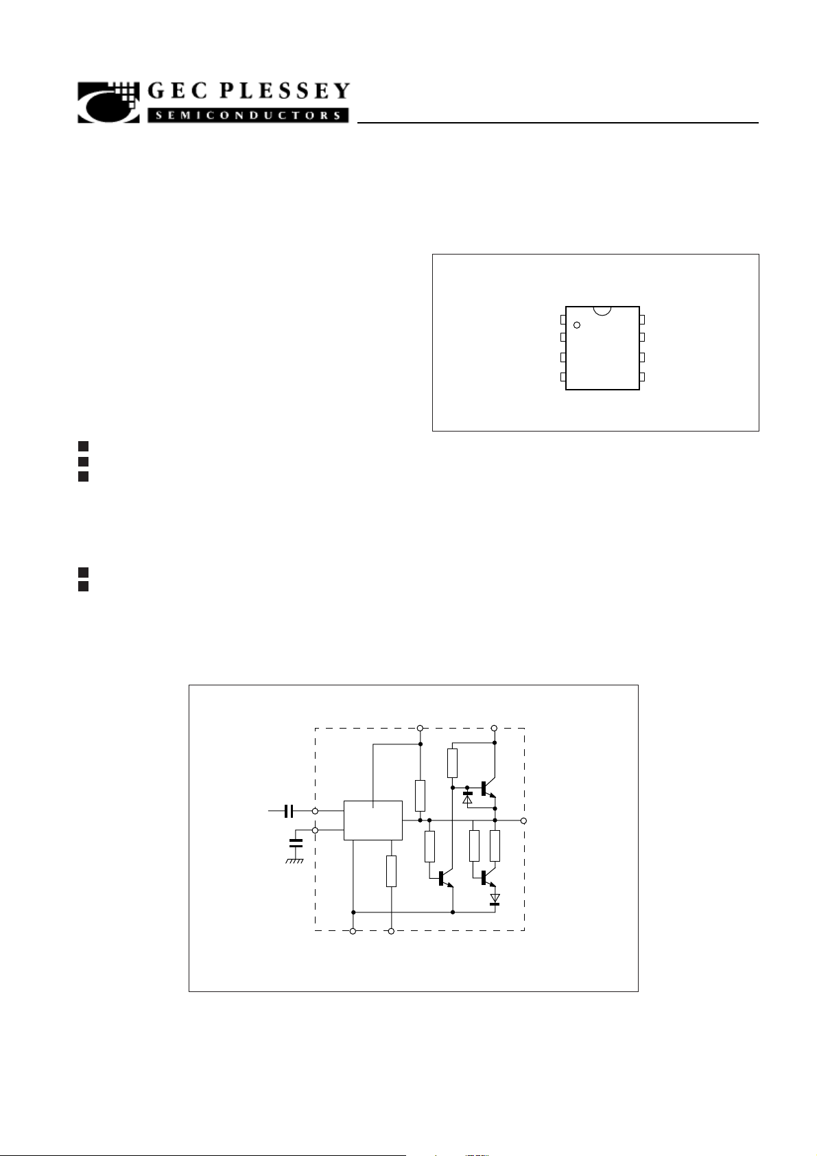
MODULUS CONTROL UNIT 1 Vcc 8
OUTPUT Vcc 2 NO CONNECTION7
OUTPUT 3 INPUT6
0V 4 INPUT DECOUPLING5
SP
8716/8/9
DS 3292 -1
FEATURES
DC to 520MHz Operation
-40°C to +85°C Temperature Range
Control Inputs and Outputs are CMOS Compatible
QUICK REFERENCE DATA
Supply Voltage 5.0V ± 0.25V
Supply Current 10.5mA typ.
SIGNAL
INPUT
6
5
÷P/P + 1
Figure : 1 Pin connections - top view
ABSOLUTE MAXIMUM RATINGS
Supply voltage pin 2 or 8): 8V
Storage temperature range: -55°C to +150°C
Max. Junction temperature: +175°C
Max. clock I/P voltage: 2.5V p-p
Vcc
8
1.5k 1k 300
Vcc
2
7k
3 OUTPUT
DP8, MP8
4
0V1MODULUS
CONTROL
INPUT
Figure 2 : Functional diagram
Page 3
SP8716/8/9
ELECTRICAL CHARACTERISTICS
Test conditions (unless otherwise stated):]
Supply voltage: Vcc = +4/95 to 5.45V, Temperature: T
amb = -40°C to +85°C
Characteristics
Max. frequency
Min. frequency (sinewave input)
Power supply current
Output high voltage
Output low voltage
Control input high voltage
Control input low voltage
Control input high current
Control input low current
Clock to output delay
Set-up time
Release time
NOTES
1. Tested at 25°C only
2. Guaranteed but not tested
Symbol
f
max
fmin
ICC
VOH
VOL
VINH
VINL
VINH
VINL
p
t
ts
tr
Min.
520
cc - 1.2)
(V
-0.20
3.3
0
10
10
Value
Max.
30
11.9
1
8
1.7
0.41
28
Units
MHz
MHz
mA
V
V
V
V
mA
mA
ns
ns
ns
Conditions
Input 100-280mV p-p
Input 400-800mV p-p
L = 3pF; pins 2, 8 linked
C
L = -0.2mA
I
L = 0.2mA
I
÷P
÷P +1
INH = 8V
V
V
INL = 0V
L = 10pF
C
L = 10pF
C
C
L = 10pF
Notes
1
2
1
1
1
1
1
1
1
2
2
2
NOTE
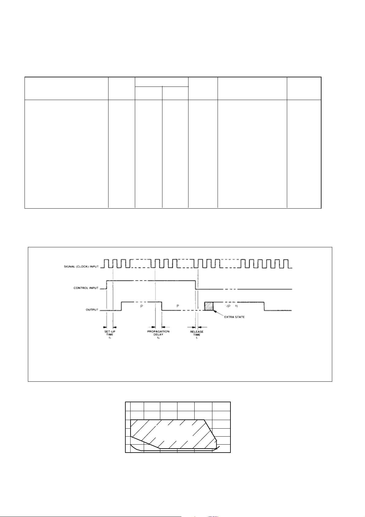
The set-up time ts is defined as the minimum time that can elapse between a L → H transition of the control input
and the next L → H clock pulse transition to ensure that the ÷P mode is obtained.
The release time tr is defined as the minimum time that can elapse between a H → L transition of the control input
and the next L → H clock pulse transition to ensure that the ÷(P +1) mode is obtain
Figure 3 : Timing diagram
1000
800
600
400
200
INPUT AMPLITUDE (mV p-p)
0
30 100 200 300 400 500
Figure 4 : Typical input characteristics
GUARANTEED *
OPERATING
WINDOW
FREQUENCY IN MHz
280mV
520mV
*Tested as
specified in
table of
Electrical
Characteristics
Page 4
OPERATING NOTES
SP8716/8/9
1. The inputs are biased internally and coupled to a signal
source with suitable capacitors.
2. If no signal is present the devices will self-oscillate. If this
is undesirable it may be prevented by connecting a 15k
resistor from one input to pin 4 (ground). This will reduce the
sensitivity.
3. The circuits will operate down to DC but slew rate must
be better than 100V/,us.
4. The output stage is of an unusual design and is intended
to interface with CMOS. External pull-up resistors or circuits
must not be used.
5. This device is NOT suitable for driving TTL or its
derivatives.
CONTROL
INPUT
OUTPUT
1
2
3
4
8
7
6
1n
5
1n
0V
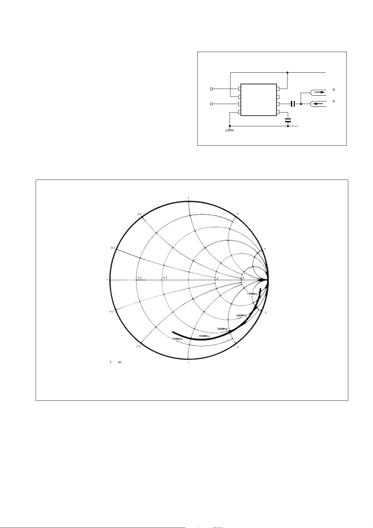
Figure 5: Toggle frequency test circuit
Vcc
50
MONITOR
50
SIGNAL
SOURCE
Figure 6 : Typical input impedance
 Loading...