

Page 1
1
SP8715
SP8715
1100MHz Very Low Current Multi-Modulus Divider
Description
The SP8715 is a switchable divide by 64/65, 128/129
programmable divider which is guaranteed to operate up
to 1100MHz. It will operate from a supply of 2.7V to 5.25V
and requires typically 3.6mA (including the output current).
It also features a power down facility for battery economy.
The RF inputs are internally biased and should be
capacitively coupled to the signal source. The output is
designed to interface with CMOS synthesisers.
Features
● Operation to 1100MHz
● Very Low Power
● Single Supply Operation 2.7V to 5.25V
● Power Down Facility for Battery Economy
● Latched Modulus Control Input
● Push Pull Output Drive
● ESD Protection on All Pins
†
DS3830 Issue 4.2 September 1999
Applications
● Cellular Telephones
● Cordless Telephones
● Mobile Radio
†
ESD precautions must be observed
Odering Information
SP8715/IG/MPAS Industrial Temperature Range
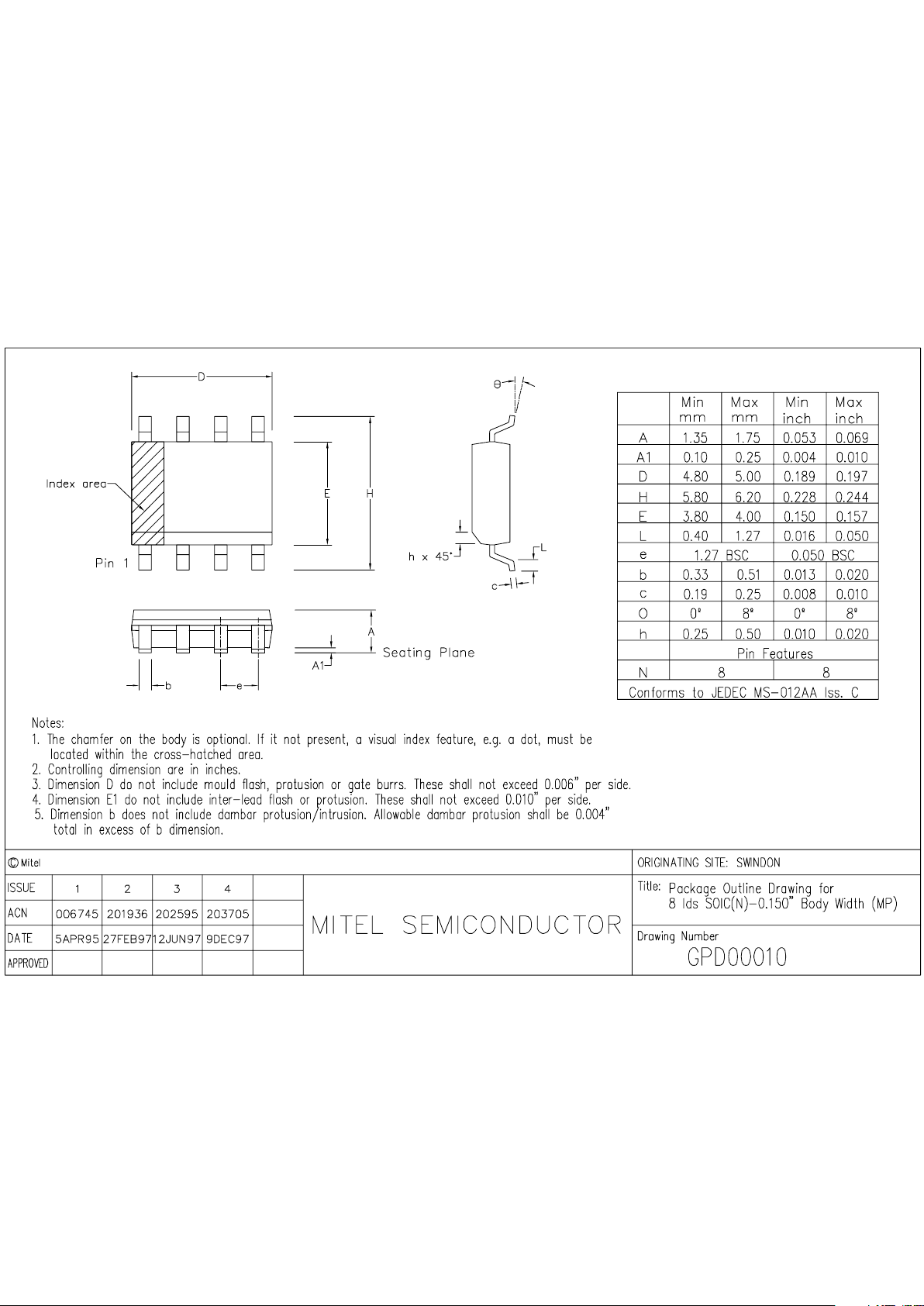
Miniature Plastic SOIC Package
SP8715/IG/MPAC As Above supplied on Tape
and Reel
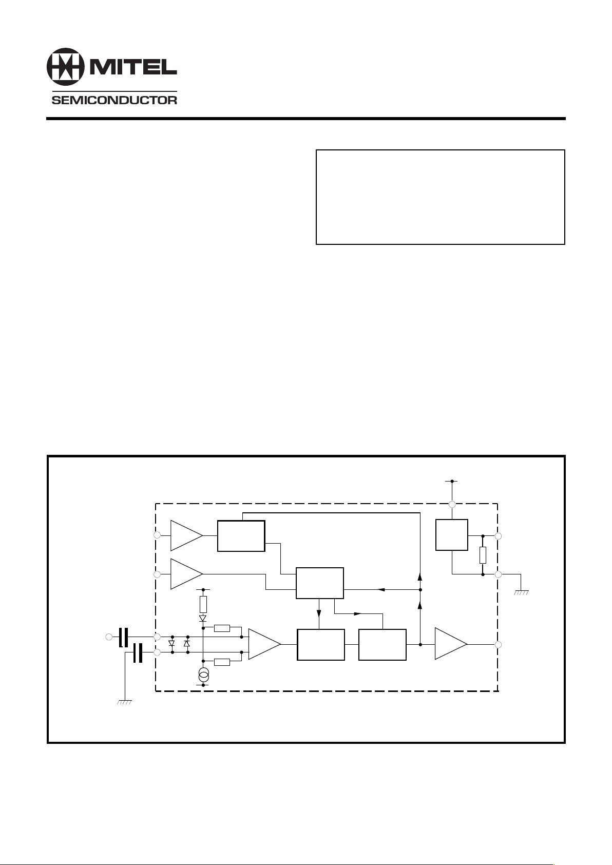
BIAS
V
CC
2
7
5
250K
NOMINAL
4
CK
D
Q
6
3
VCCV
EE
1
8
V
EE
POWER
DOWN
OUTPUT
MC
RS
RF
INPUT
(CLOCK)
DIVIDE BY
4 / 5
DIVIDE BY
16 / 32
CONTROL
LOGIC
D TYPE
Figure 1 Block Diagram
Page 2
2
SP8715
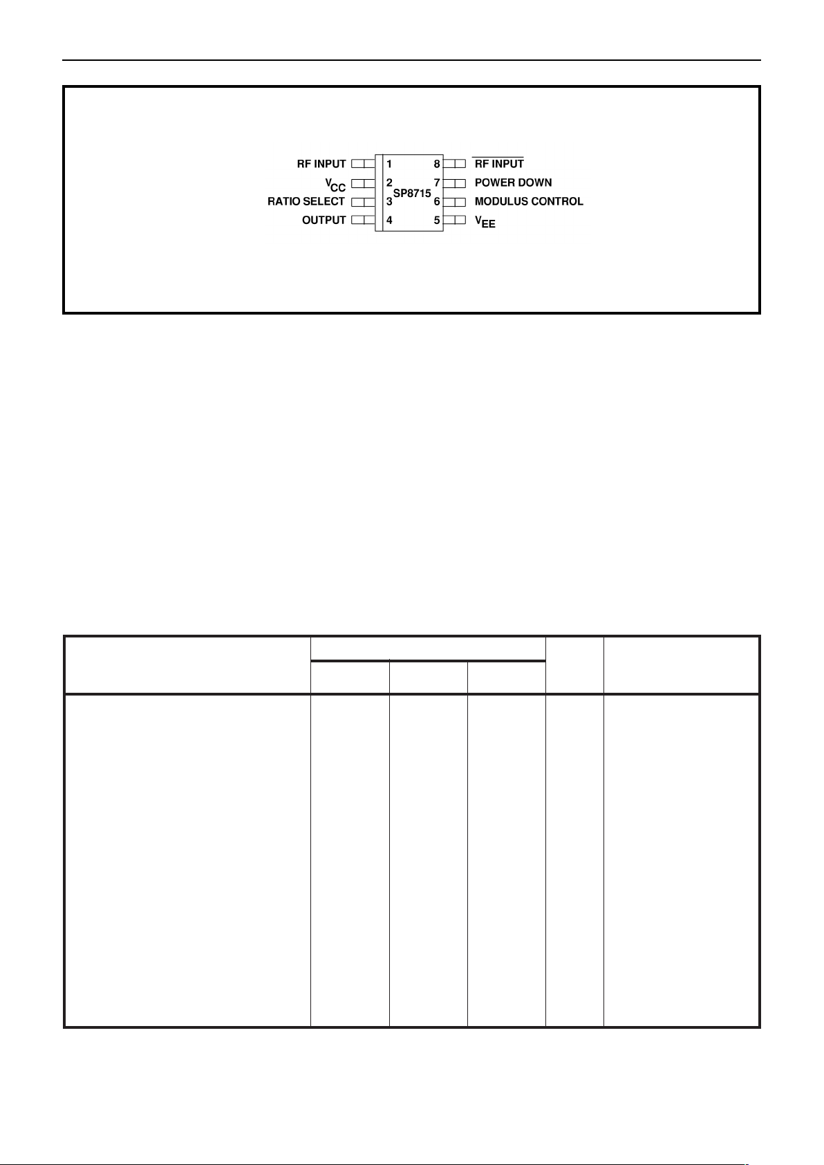
Figure 2 Pin Connections
MP8
Absolute Maximum Ratings
Supply voltage (VEE=0V) (note 1) -0.5V to 7V
Control and RF inputs,
RF output (VEE =0V) (note 1)-0.5V to VCC+0.5V
RF input current (note 1) 10mA
Operating temperature -40°C to +85°C
Storage temperature range -55°C to +150°C
Maximum junction temperature +150°C
NOTE 1. Duration <2 minutes.
Electrical Characteristics
Guaranteed over the following conditions (unless otherwise stated):
VCC=+2.7V to +5.25V (with respect to VEE), Output load (pin 4) = 10pF, T
amb
= -40°C to +85°C (note 2)
Characteristic Units Conditions
Supply current (note 3) 3.6 4.2 mA Power down input low
Supply current (note 3) 8 50 µA Power down input high
Power down high VCC-0.5 V
CC
V
Power down low 0 VCC-2.0 V
Modulus control high (note 4) 0.6V
CC
V
CC
V Divide by 64 or 128
Modulus control low (note 4) 0 0.4V
CC
V Divide by 65 or 129
Ratio select high (note 4, 9) 0.6V
CC
V
CC
V Divide by 64 or 65
Ratio select low (note 4, 9) 0 0.4V
CC
V Divide by 128 or 129
Max. sinewave input frequency 1100 MHz See Figure 5
Min. sinewave input frequency 200 MHz See Figure 5
Min. RF input voltage 50 mV RMS RF input 200MHz to
1100MHz. See Figure 5
Max. RF input voltage 200 mV RMS RF input 200MHz to
1100MHz. See Figure 5
Value
Min. Typ. Max.
Page 3
3
SP8715
Electrical Characteristics (Continued)
Guaranteed over the following conditions (unless otherwise stated):
VCC=+2.7V to +5.25V (with respect to VEE), Output load (pin 4) = 10pF, T
amb
= -40°C to +85°C (note 2)
Characteristic Units Conditions
Output level (pin 4) 500 600 mV p-p
Modulus set-up time, ts(notes 5,6,8) 20 ns RF input = 1GHz
Modulus hold time, t
h
(notes 6,8) 1 ns RF input = 1GHz
Power down time, t
pd
(notes 7,8) 10 µs See Figure 9
Power down recovery time, t
pu
6 µs See Figure 9
(notes 7,8)
NOTES
2. All electrical testing is performed at +85°C.
3. Typical values are measured at +25°C and VCC = +5V.
4. Modulus Control and Ratio Select are high impedance inputs which can be driven directly by standard
CMOS outputs.
5. Modulus control is latched at the end of the previous cycle.
6. See Figure 4.
7. See Figure 8.
8. These parameters are not tested but are guaranteee by design.
9. The ratio select pin is not intended to be switched dynamically.
Value
Min. Typ. Max.
OPERATING NOTES
The RF inputs are biased internally and are normally
coupled to the signal source with suitable capaitors.
The output stage has a novel design and is intended
to drive a CMOS synthesiser input. External pull-down
resistors or circuits are not required. The SP8715 is
not suitable for driving TTL or similar devices.
The device will operate down to DC frequencies for
non-sinusoidal signals provided that the input slew
rate is better than 100V/µs.
POWER DOWN (pin 7) is connected internally to a
pull-down resistor. If the battery economy facility is not
used, pin 7 should be either left unconnected or
connected to VEE.
Page 4
4
SP8715
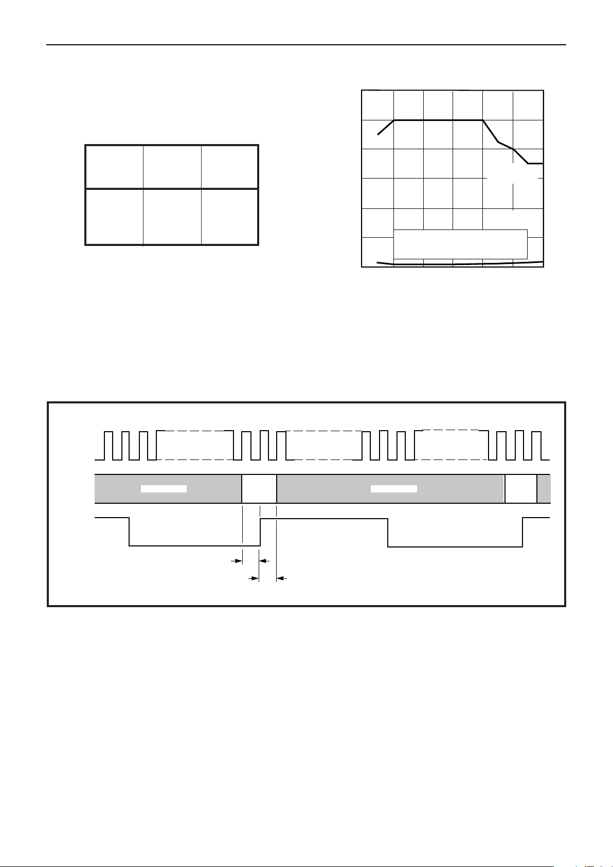
Figure 3 Typical Input Characteristics
Ratio Modulus Division
Select Control Ratio
(Pin 3) (Pin 6)
L L 129
L H 128
HL65
HH64
TYPICAL
SENSITIVITY
TYPICAL
OVERLOAD
1000
800
600
400
200
0
200 400 600 800 1000 1200
* Tested as specified in table of Electrical Characteristics
FREQUENCY (MHZ)
RF INPUT VOLTAGE (mV RMS)
GUARANTEED*
OPERATING WINDOW
Table 1 Truth Table
Figure 4 Modulus Control Timing Diagram
RF INPUT
CLOCK
MODULUS
CONTROL
INPUTS
OUTPUT
t
s
t
h
32 (64)
32 (64)
or 33 (65
)
DON'T CARE
DON'T CARE
Page 5
5
SP8715
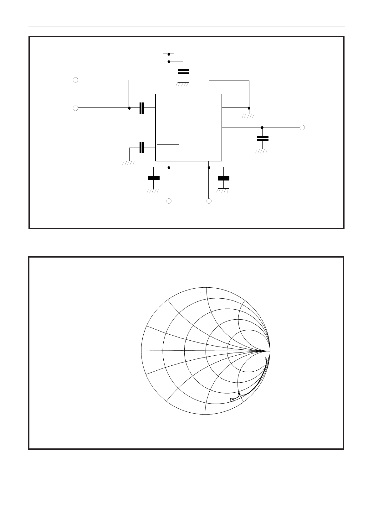
Figure 5 Toggle Frequency Test Circuit
Figure 6 Typical S11 parameter for pin 1. VCC = +5.0V
j0.2
j0.5
j1
S11
PLOT 50 OHM
NORMALISED
f1: 130MHz
f2: 1310MHz
j2
-j0.2
-j0.5 -j2
-j1
f1
f2
0.2 0.5 1 2
V
CC
V
CC
RF INPUT
POWER
DOWN
RATIO
SELECT
MC
RF INPUT
OUTPUT
MODULUS
CONTROL 1 INPUT
1n
1n
10n 10n
100n
C
L
50‰
MONITOR
50‰
SIGNAL
SOURCE
SP8715
OUTPUT
MODULUS
CONTROL 2 INPUT
V
EE
Page 6
6
SP8715
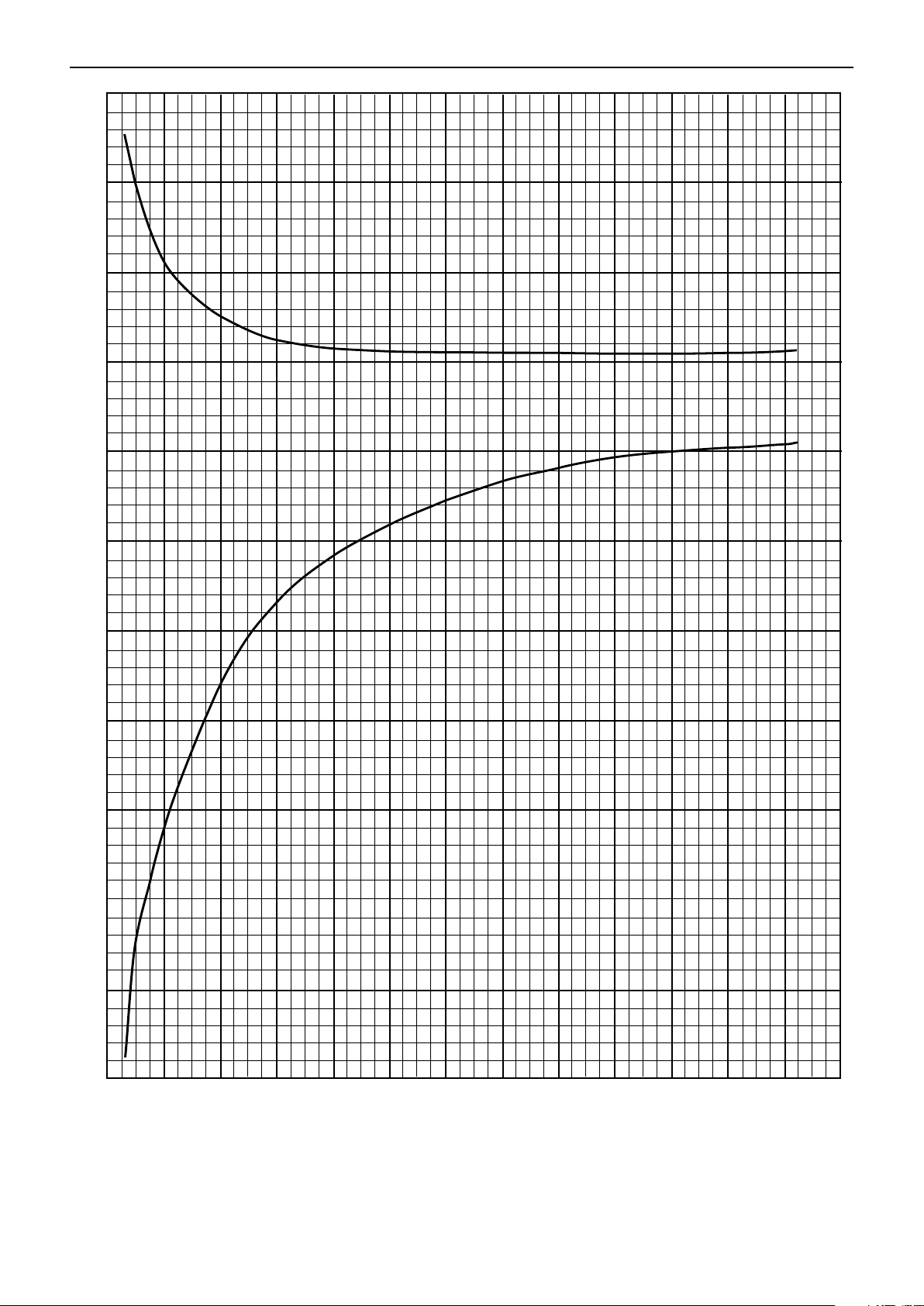
Figure 7 Typical Input Impedance v. Frequency
300
200
100
0
-100
-200
-300
-400
-500
-600
-700
-800
100 200 300 400 500 600 700 800 900 1000 1100 1200 1300 1400
INPUT FREQUENCY (MHz)
jx ( )
R( )
Page 7
7
SP8715
FREQ-MHZ
130.000
153.600
177.200
200.800
224.400
248.000
271.600
295.200
318.800
342.400
366.000
389.600
413.200
436.800
460.400
484.000
507.600
531.200
554.800
578.400
602.000
625.600
649.200
672.800
696.400
720.000
743.600
767.200
790.800
814.400
838.000
861.600
885.200
908.800
932.400
956.000
979.600
1003.20
1026.80
1050.40
1074.00
1097.60
1121.20
1144.80
1168.40
1192.00
1215.60
1239.20
1262.80
1286.40
1310.00
jx (Ω)
-733.538
-688.623
-583.339
-545.839
-482.377
-441.798
-411.502
-369.645
-346.620
-323.129
-304.804
-280.556
-269.674
-255.279
-245.161
-234.680
-224.572
-211.375
-203.241
-194.613
-186.545
-182.049
-174.839
-168.320
-160.468
-156.267
-149.642
-145.328
-143.144
-137.557
-132.750
-129.254
-124.495
-120.568
-118.100
-113.395
-109.552
-105.975
-103.110
-99.886
-98.149
-98.605
-99.907
-100.925
-99.639
-98.425
-95.033
-92.553
-89.249
-86.081
-82.581
R (Ω)
255.068
153.362
153.330
115.187
88.649
80.815
71.050
56.207
39.526
41.338
38.779
39.210
23.809
21.221
27.545
23.333
22.227
19.931
17.767
17.636
14.607
12.479
13.075
12.891
12.583
11.250
10.213
10.187
11.269
11.081
10.509
10.063
10.172
10.745
10.841
10.884
12.260
12.984
14.508
16.625
19.260
22.799
23.285
21.149
18.956
16.434
14.377
13.743
12.711
12.776
12.598
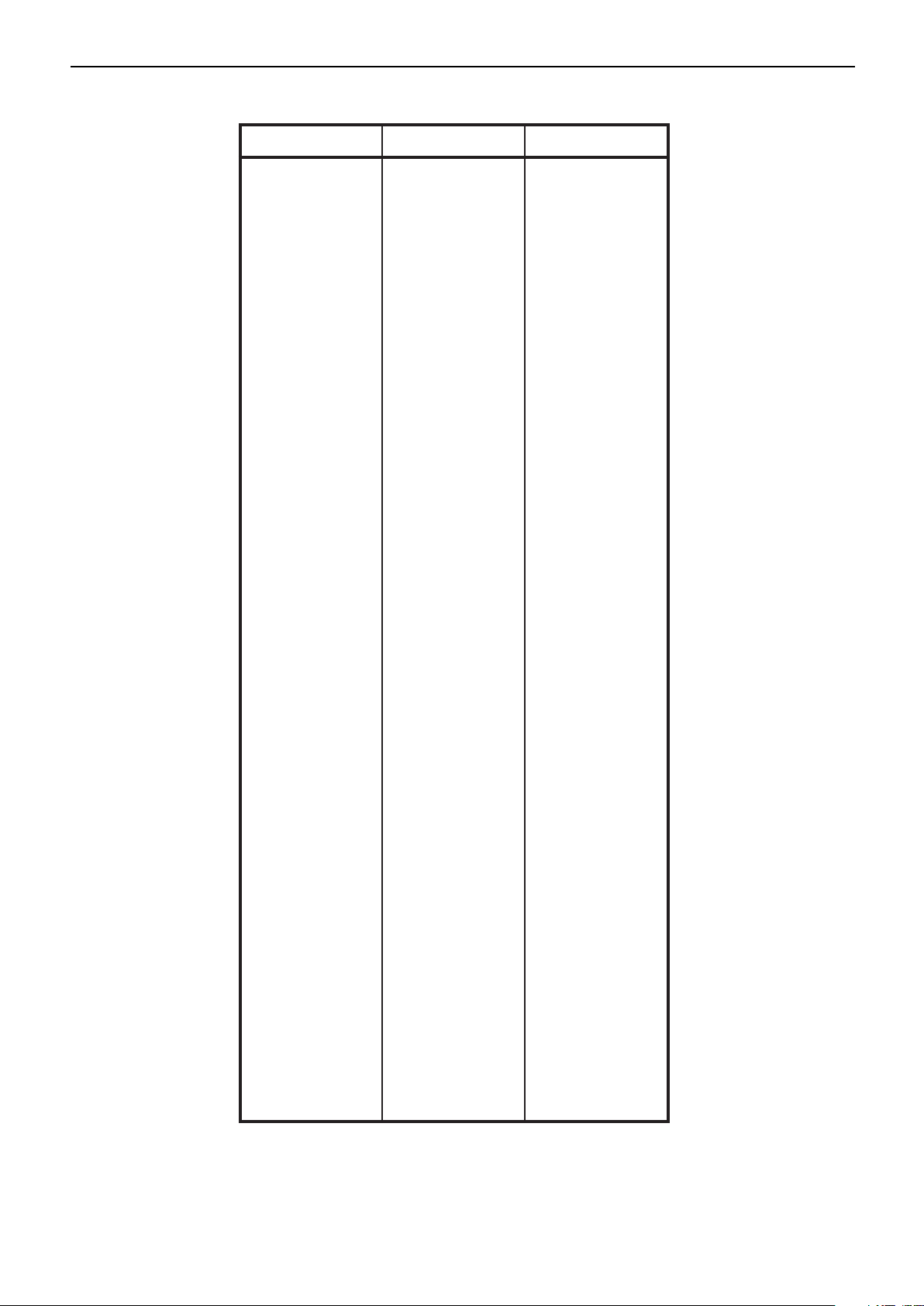
Table.2 Coefficients for Figure 7
Page 8
8
SP8715
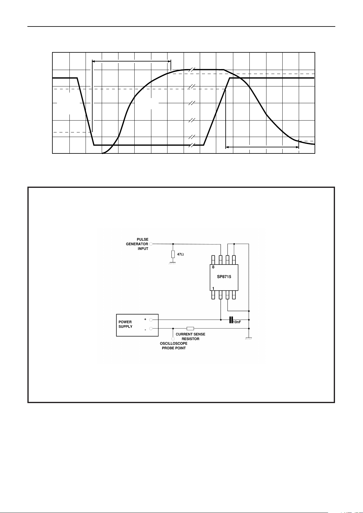
Figure 8 Power Up and Power Down
Figure 9 Power-Down Time Test Circuit
t
pu
t
pd
SUPPLY
CURRENT
POWER
DOWN
INPUT
VOLTAGE
CC
V - 0.5V
0.05
I
C
CURRENT
VOLTAGE
TIME
0.95
I
C
CC
V - 2.0V
Page 9
Page 10

M Mitel (design) and ST-BUS are registered trademarks of MITEL Corporation
Mitel Semiconductor is an ISO 9001 Registered Company
Copyright 1999 MITEL Corporation
All Rights Reserved
Printed in CANADA
TECHNICAL DOCUMENTATION - NOT FOR RESALE
World Headquarters - Canada
Tel: +1 (613) 592 2122
Fax: +1 (613) 592 6909
North America Asia/Pacific Europe, Middle East,
Tel: +1 (770) 486 0194 Tel: +65 333 6193 and Africa (EMEA)
Fax: +1 (770) 631 8213 Fax: +65 333 6192 Tel: +44 (0) 1793 518528
Fax: +44 (0) 1793 518581
http://www.mitelsemi.com
Information relating to products and services furnished herein by Mitel Corporation or its subsidiaries (collectively “Mitel”) is believed to be reliable. However, Mitel assumes no
liability for errors that may appear in this publication, or for liability otherwise arising from the application or use of any such information, product or service or for any infringement of
patents or other intellectual property rights owned by third parties which may result from such application or use. Neither the supply of such information or purchase of product or
service conveys any license, either express or implied, under patents or other intellectual property rights owned by Mitel or licensed from third parties by Mitel, whatsoever.
Purchasers of products are also hereby notified that the use of product in certain ways or in combination with Mitel, or non-Mitel furnished goods or services may infringe patents or
other intellectual property rights owned by Mitel.
This publication is issued to provide information only and (unless agreed by Mitel in writing) may not be used, applied or reproduced for any purpose nor form part of any order or
contract nor to be regarded as a representation relating to the products or services concerned. The products, their specifications, services and other information appearing in this
publication are subject to change by Mitel without notice. No warranty or guarantee express or implied is made regarding the capability, performance or suitability of any product or
service. Information concerning possible methods of use is provided as a guide only and does not constitute any guarantee that such methods of use will be satisfactory in a specific
piece of equipment. It is the user’s responsibility to fully determine the performance and suitability of any equipment using such information and to ensure that any publication or
data used is up to date and has not been superseded. Manufacturing does not necessarily include testing of all functions or parameters. These products are not suitable for use in
any medical products whose failure to perform may result in significant injury or death to the user. All products and materials are sold and services provided subject to Mitel’s
conditions of sale which are available on request.
 Loading...