

Page 1
®
1
2
3
4
5
6
7
8
9
10
11
12
13
14
15
16
17
18
19
20
21
22
23
24
25
26
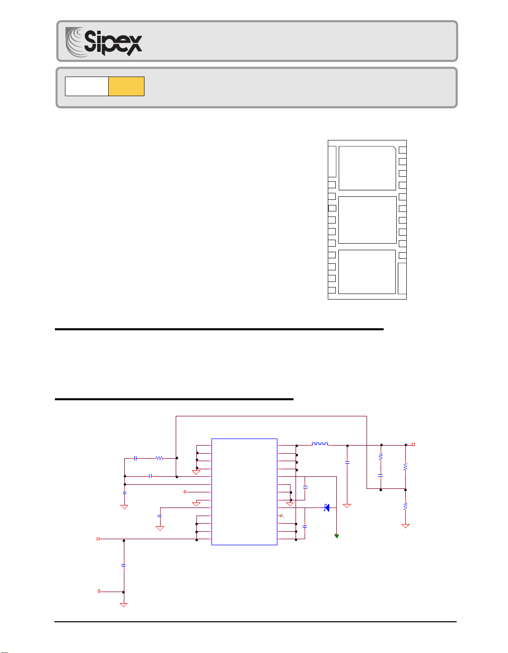
TOP VIEW
Heatsink Pad 1
Connect to Lx
Heatsink pad 2
Connect to GND
Heatsink pad 3
Connect to V
IN
P
GND
P
GND
GND
V
FB
COMP
UVIN
GND
SS
V
IN
LX
LX
LX
LX
V
CC
GND
GND
GND
BST
NC
LX
LX
LX
DFN PACKAGE
7mm x 4mm
SP7650
P
GND
V
IN
V
IN
V
IN
Blox
M
Preliminary
T
Wide Input Voltage Range 3A, 300kHz,
Power
FEATURES
■ 2.5V to 28V Step Down Achieved Using Dual Input
■ Output Voltage down to 0.8V
■ 3A Output Capability
■ Built in Low R
■ Highly Integrated Design, Minimal Components
■ 300 kHz Fixed Frequency Operation
■ UVLO Detects Both V
■ Over Temperature Protection
■ Short Circuit Protection with Auto-Restart
■ Wide BW Amp Allows Type II or III Compensation
■ Programmable Soft Start
■ Fast Transient Response
■ High Efficiency: Greater than 95% Possible
■ Asynchronous Start-Up into a Pre-Charged Output
■ Small 7mm x 4mm DFN Package
Blox
Power Switches (40 mΩ typ)
DSON
Buck Regulator
and V
CC
IN
SP7650
Now Available in Lead Free Packaging
DESCRIPTION
The SP7650 is a synchronous step-down switching regulator optimized for high efficiency. The part is designed to be
especially attractive for dual supply, 12V or 24V distributed power systems step down with 5V used to power the
controller. This lower VCC voltage minimizes power dissipation in the part and is used to drive the top switch. The SP7650
is designed to provide a fully integrated buck regulator solution using a fixed 300kHz frequency, PWM voltage mode
architecture. Protection features include UVLO, thermal shutdown and output short circuit protection. The SP7650 is
available in the space saving DFN package.
U1
SP7650
1
PGND
RZ2
CZ2
CF1
VIN
12V
GND
100pF
Date: 2/18/05 SP7650 Wide Input Voltage Range 3A, 300kHz, Buck Regulator © Copyright 2005 Sipex Corporation
1,000pF
C1
22uF
16V
CP1
22pF
15k,1%
ENABLE
CSS
47nF
2
PGND
3
PGND
4
GND
5
VFB
6
COMP
7
UVIN
8
GND
9
SS
10
VIN
11
VIN
12
VIN
13
VIN
VCC
GND
GND
GND
fs=300Khz
Notes:
1. U1 Bottom-Side Layout should
has three contacts isolated from
one another Vin SWNODE and GND
2. RSET=54.48/(Vout-0.8V) (KOhm)
1
TYPICAL APPLICATION CIRCUIT
26
LX
25
LX
24
LX
23
LX
22
21
20
19
18
BST
17
NC
16
LX
15
LX
14
LX
L1
4.7uH, Irate=4.78A
CVCC
2.2uF
DBST
SD101AWS
CBST
6800pF
+5V VCC
C3
47uF
6.3V
RZ3
7.15k,1%
CZ3
150pF
R1
68.1k,1%
RSET
21.5k,1%
(note 2)
VOUT
3.3V
0-3A
Page 2
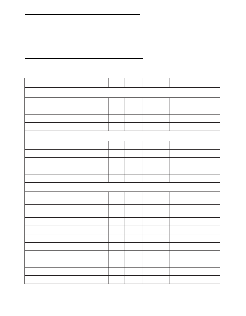
These are stress ratings only and functional operation of the device at
these ratings or any other above those indicated in the operation sections
of the specifications below is not implied. Exposure to absolute maximum
rating conditions for extended periods of time may affect reliability.
.................................................................................................. 7V
V
CC
...........................................................................................................................................
V
IN
...............................................................................................................................................
I
LX
BST ............................................................................................... 35V
BST-SWN ......................................................................... -0.3V to 7V
SWN ................................................................................... -1V to 30V
30V
5A
GH ......................................................................... -0.3V to BST+0.3V
GH-SWN ......................................................................................... 7V
All other pins .......................................................... -0.3V to V
Storage Temperature .................................................. -65°C to 150°C
Power Dissipation ...................................... Internally Limited via OTP
ESD Rating .......................................................................... 2kV HBM
Thermal Resistance ϑ
....................................................................................
JC
ELECTRICAL SPECIFICATIONS
ABSOLUTE MAXIMUM RATINGS
Unless otherwise specified: -40°C < T
LX = GND = 0V, UVIN = 3.0V, CV
The ♦ denotes the specifications which apply over the full temperature range, unless otherwise specified.
RETEMARAP.NIM.PYT.XAMSTINUSNOITIDNOC
TNERRUCTNECSEIUQ
< 85°C, -40°C< Tj< 125°C, 4.5V < V
AMB
= 1µF, C
CC
= 0.1µF, CSS = 50nF, Typical measured at V
COMP
< 5.5V, 3V< Vin< 28V, BST=LX + 5V,
CC
CC
= 5V.
+0.3V
CC
5°C/W
V
CC
V
CC
)gnihctiwsoN(tnerruCylppuS5.13 AmVBFV9.0=
)gnihctiws(tnerruCylppuS46Am
♦
)gnihctiwsoN(tnerruCylppuSTSB2.04.0AmV
)gnihctiws(tnerruCylppuSTSB446Am
♦
V9.0=
BF
OLVU:NOITCETORP
V
CC
V
CC
dlohserhTtratSOLVU00.452.45.4V
siseretsyHOLVU001002003Vm
dlohserhTtratSNIVU3.25.256.2V
♦
siseretsyHNIVU002003004Vm
tnerruCtupnINIVU1AµV0.3=NIVU
ECNEREFERREIFILPMARORRE
ecnerefeRreifilpmArorrE297.0008.0808.0V
ecnerefeRreifilpmArorrE
erutarepmeTdnaeniLrevO
887.0008.0218.0V
♦
V
BFV;CC
erusaeM,.gifnoCniaGX2
Cº52=T,V5=
ecnatcudnocsnarTreifilpmArorrE6V/Am
niaGreifilpmArorrE06BddaoLoN
tnerruCkniSPMOC051AµV
tnerruCecruoSPMOC051AµV
V
BF
tnerruCsaiBtupnI05002AnVBFV8.0=
BF
BF
V9.0=PMOC,V9.0=
V2.2=PMOC,V7.0=
eloPlanretnI4zHM
pmalCPMOC5.2VV
BF
Cº52=AT,V7.0=
tneiciffeoC.pmeTpmalCPMOC2-Cº/Vm
Date: 2/18/05 SP7650 Wide Input Voltage Range 3A, 300kHz, Buck Regulator © Copyright 2005 Sipex Corporation
2
Page 3
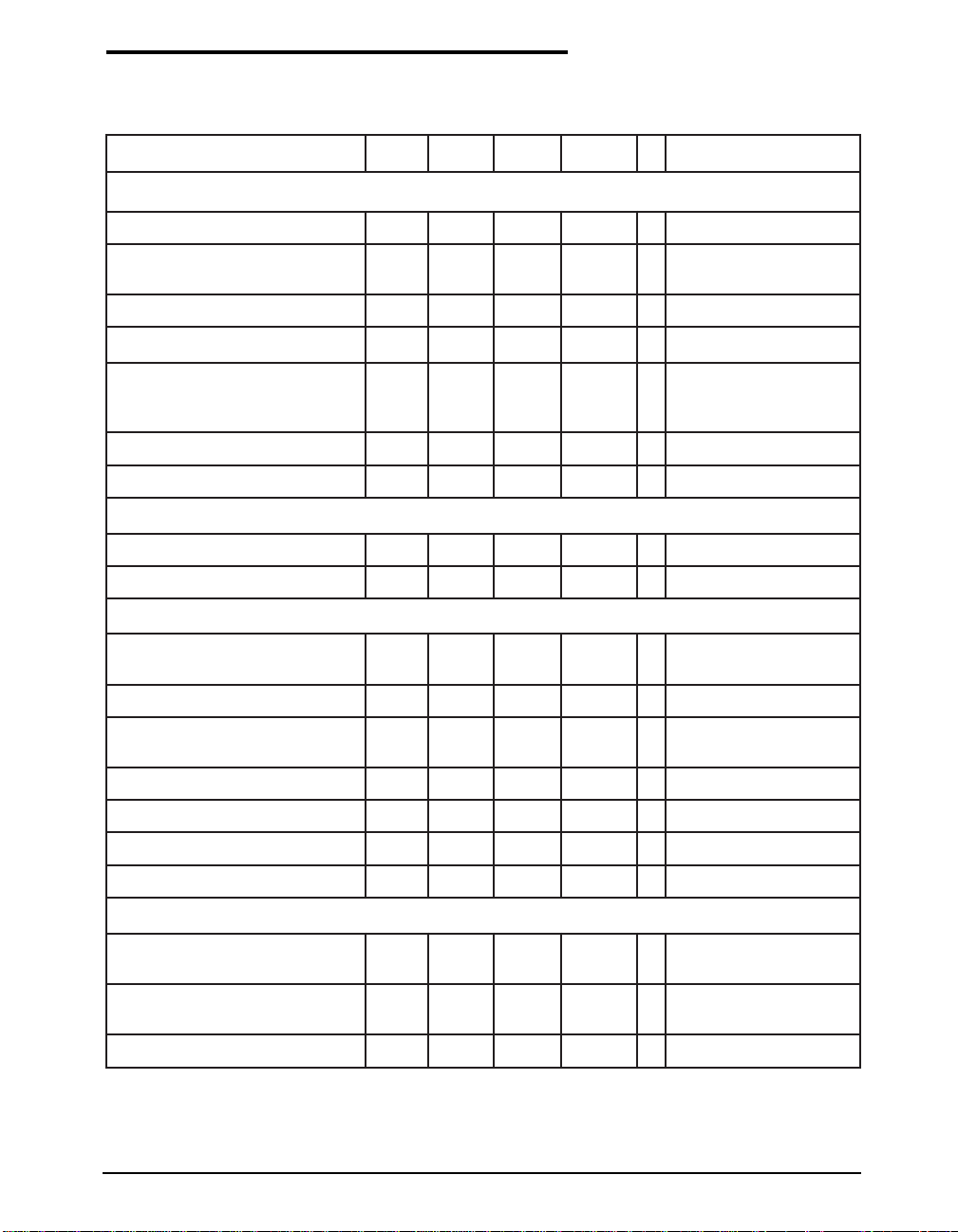
Unless otherwise specified: -40°C < T
LX = GND = 0V, UVIN = 3.0V, CV
The ♦ denotes the specifications which apply over the full temperature range, unless otherwise specified.
RETEMARAP.NIM.PYT.XAMSTINUSNOITIDNOC
edutilpmApmaR29.01.182.1V
< 85°C, -40°C< Tj< 125°C, 4.5V < V
AMB
= 1µF, C
CC
= 0.1µF, CSS = 50nF, Typical measured at V
COMP
< 5.5V, 3V< Vin< 28V, BST=LX + 5V,
CC
CC
= 5V.
HTAPYALEDPOOL&PMAR,ROTARAPMOCMWP:POOLLORTNOC
ELECTRICAL SPECIFICATIONS
T
tesffOPMAR1.1V
A
tneiciffeoC.pmeTtesffoPMAR2-Cº/Vm
htdiWesluPmuminiMHG09081sn
♦
oitaRytuDelballortnoCmumixaM2979%
oitaRytuDmumixaM001%selcyc02rofdilaV
oitaRrotallicsOlanretnI042003063zHk
♦
TRATSTFOS:SREMIT
:tnerruCegrahCSS01Aµ
:tnerruCegrahcsiDSS1Am
♦
lamrehT&tiucriCtrohS:NOITCETORP
egatloVdlohserhTtiucriCtrohS2.052.03.0V
♦
V
BF
tuoemiTpucciH002smVBFV5.0=
elcyCytuD%001ta
selcyCkcolCelbawollAforebmuN
selcyC02retfAesluPLGmuminiM5.0selcyCV
erutarepmeTnwodtuhSlamrehT541CºV
02selcyC
BF
BF
erutarepmeTyrevoceRlamrehT531Cº
PMOCPMAR,Cº52=
gnihctiwSstratsHGlitnu
oitaRytuDmumixaM
erofebtsujderusaeM
snigebgnislup
V2.0=SS,tneserPtluaF
VderusaeM
-)V8.0(
FER
V7.0=
V7.0=
siseretsyHlamrehT01Cº
EGATSREWOP:TUPTUO
V
RhctiwSediShgiH
NOSD
RhctiwSediswoLsuorhcnyS
NOSD
04 Ωm
04 Ωm
CC
T
V
CC
T
I;V5=
A3=
TUO
Cº52=
BMA
I;V5=
A3=
TUO
Cº52=
BMA
tnerruCtuptuOmumixaM3A
Date: 2/18/05 SP7650 Wide Input Voltage Range 3A, 300kHz, Buck Regulator © Copyright 2005 Sipex Corporation
3
Page 4
#niPemaNniPnoitpircseD
3-1P
12-91,8,4DNG
5V
6PMOC
7NIVU
9SS
31-01V
62-32,61-41XLVdnanipsihtneewtebrotcudninatcennoC
22V
71CNtcennoCoN
DNG
BF
VU
NI
CC
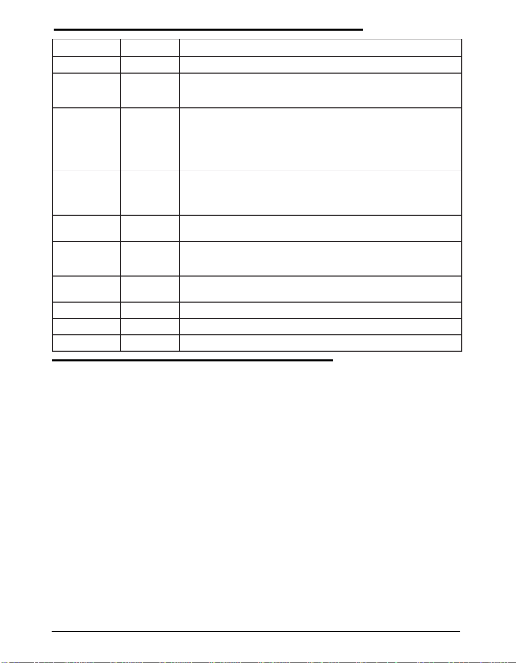
PIN DESCRIPTION
reifitcersuonorhcnysehtrofnoitcennocdnuorG
erarevirdrewoprewoldnaCIehtfoyrtiucriclortnocehT.niPdnuorG
.tuoCfolanimret
VrevenehW.redividrotsiserlanretxenahguorht
BF
.edom
Vrodnuorgrehtiednanipsihtotdetcennoc
.pooledom
NI
ylppussaibV5lanretxeroftupnI
BF
VneewtebredividrotsiseratcennoC.egatlovniVroftupniOLVU
egatlovgnitarepomuminimtesot
.snoitidnoctluafllagnirudtnerruc)nim(Am1aaiv
.DNGPdnanipsihtneewtebroticapac
TUO
NI
)-(ehtotsecartdnuorgrehtomorfyletarapesnruteR.nipsihtotdecnerefer
tupnignitrevniehtsitI.nipnoitceteDtiucriCtrohSdnaegatloVkcabdeeF
roftniopkcabdeefegatlovtuptuoehtsasevresdnareifilpmArorrEehtfo
detsujdaebnacdnadesnessiegatlovtuptuoehT.retrevnoCkcuBeht
ehtwolebV52.0spord
puccihsretneCIehtdnadetcetedsitluaftiucrictrohsa,ecnereferevitisop
tupnignitrevniehtotdetcennocyllanretnisitI.reifilpmArorrEehtfotuptuO
dnanesohcsinoitanibmocretliflamitponA.rotarapmocMWPehtfo
egatlovehtezilibatsot
dna
ehttesotDNGdnaSSneewtebroticapaclanretxenatcennoC.tratStfoS
woldlehsinipSSehT.tnerrucecruosAµ01ehtnodesabetartratstfos
gnilpuocedaecalP.TEFSOMlennahc-NedishgihehtotnoitcennoctupnI
THEORY OF OPERATION
General Overview
The SP7650 is a fixed frequency, voltage mode,
synchronous PWM regulator optimized for high
efficiency. The part has been designed to be
especially attractive for high voltage applications utilizing 5V to power the controller and
2.5V to 28V for step down conversion.
The SP7650 contains two unique control features that are very powerful in distributed applications. First, asynchronous driver control is
enabled during start up, to prohibit the low side
switch from pulling down the output until the
high side switch has attempted to turn on. Second, a 100% duty cycle timeout ensures that the
The heart of the SP7650 is a wide bandwidth
transconductance amplifier designed to accommodate Type II and Type III compensation
schemes. A precision 0.8V reference, present on
low side switch is periodically enhanced during
extended periods at 100% duty cycle. This guarantees the synchronized refreshing of the BST
capacitor during very large duty ratios.
the positive terminal of the error amplifier permits the programming of the output voltage
down to 0.8V via the VFB pin. The output of the
error amplifier, COMP, compared to a 1.1V
peak-to-peak ramp is responsible for trailing
edge PWM control. This voltage ramp, and
PWM control logic are governed by the internal
oscillator that accurately sets the PWM fre-
The SP7650 also contains a number of valuable
protection features. Programmable VIN UVLO
allows the user to set the exact value at which the
conversion voltage can safely begin down conversion, and an internal VCC UVLO which ensures that the controller itself has enough voltage to properly operate. Other protection fea-
quency to 300kHz.
Date: 2/18/05 SP7650 Wide Input Voltage Range 3A, 300kHz, Buck Regulator © Copyright 2005 Sipex Corporation
4
Page 5

THEORY OF OPERATION
tures include thermal shutdown and short-circuit detection. In the event that either a thermal,
short-circuit, or UVLO fault is detected, the
SP7650 is forced into an idle state where the
output drivers are held off for a finite period
before a restart is attempted.
Soft Start
“Soft Start” is achieved when a power converter
ramps up the output voltage while controlling
the magnitude of the input supply source current. In a modern step down converter, ramping
up the positive terminal of the error amplifier
controls soft start. As a result, excess source
current can be defined as the current required to
charge the output capacitor.
I
VIN
= C
OUT
* (DV
OUT
/ DT
SOFT-START
)
The SP7650 provides the user with the option to
program the soft start rate by tying a capacitor
from the SS pin to GND. The selection of this
capacitor is based on the 10uA pull up current
present at the SS pin and the 0.8V reference
voltage. Therefore, the excess source can be
redefined as:
IVIN = C
Under Voltage Lock Out (UVLO)
OUT
* (DV
*10µA / (CSS * 0.8V)
OUT
The SP7650 contains two separate UVLO comparators to monitor the bias (VCC) and conversion (VIN) voltages independently. The V
CC
UVLO threshold is internally set to 4.25V,
whereas the VIN UVLO threshold is programmable through the UVIN pin. When the UVIN
pin is greater than 2.5V, the SP7650 is permitted
to start up pending the removal of all other
faults. Both the VCC and V
UVLO compara-
IN
tors have been designed with hysteresis to prevent noise from resetting a fault.
Thermal and Short-Circuit
Protection
Because the SP7650 is designed to drive large
output current, there is a chance that the power
converter will become too hot. Therefore, an
internal thermal shutdown (145°C) has been
included to prevent the IC from malfunctioning
at extreme temperatures.
A short-circuit detection comparator has also
been included in the SP7650 to protect against
an accidental short at the output of the power
converter. This comparator constantly monitors
the positive and negative terminals of the error
amplifier, and if the VFB pin falls more than
250mV (typical) below the positive reference, a
short-circuit fault is set. Because the SS pin
overrides the internal 0.8V reference during soft
start, the SP7650 is capable of detecting shortcircuit faults throughout the duration of soft
start as well as in regular operation.
Handling of Faults:
Upon the detection of power (UVLO), thermal,
or short-circuit faults, the SP7650 is forced into
an idle state where the SS and COMP pins are
pulled low and both switches are held off. In the
event of UVLO fault, the SP7650 remains in this
idle state until the UVLO fault is removed.
Upon the detection of a thermal or short-circuit
fault, an internal 200ms timer is activated. In the
event of a short-circuit fault, a re-start is attempted immediately after the 200ms timeout
expires. Whereas, when a thermal fault is detected the 200ms delay continuously recycles
and a re-start cannot be attempted until the
thermal fault is removed and the timer expires.
Error Amplifier and Voltage Loop
Since the heart of the SP7650 voltage error loop
is a high performance, wide bandwidth
transconductance amplifier. Because of the
amplifier’s current limited (+/-150µA)
transconductance, there are many ways to compensate the voltage loop or to control the COMP
pin externally. If a simple, single pole, single
Date: 2/18/05 SP7650 Wide Input Voltage Range 3A, 300kHz, Buck Regulator © Copyright 2005 Sipex Corporation
5
Page 6
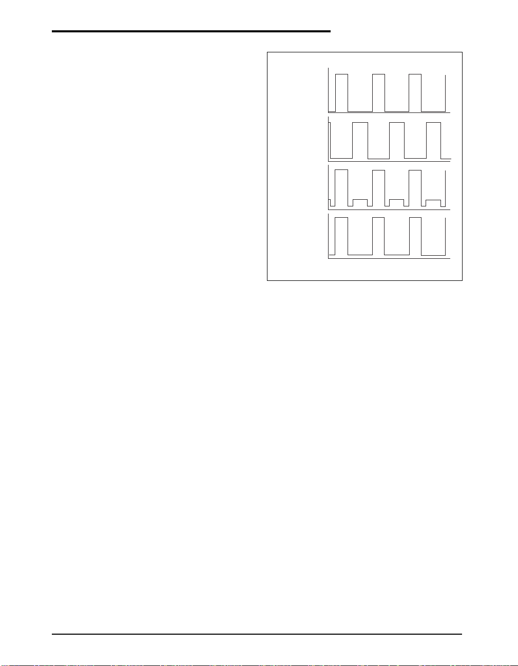
zero response is desired, then compensation can
be as simple as an RC to ground. If a more
complex compensation is required, then the
amplifier has enough bandwidth (45° at 4 MHz)
and enough gain (60dB) to run Type III compensation schemes with adequate gain and phase
margins at cross over frequencies greater than
50kHz.
The common mode output of the error amplifier
is 0.9V to 2.2V. Therefore, the PWM voltage
ramp has been set between 1.1V and 2.2V to
ensure proper 0% to 100% duty cycle capability.
The voltage loop also includes two other very
important features. One is an asynchronous start
up mode. Basically, the synchronous rectifier
can not turn on unless the high side switch has
attempted to turn on or the SS pin has exceeded
1.7V. This feature prevents the controller from
“dragging down” the output voltage during
startup or in fault modes. The second feature is
a 100% duty cycle timeout that ensures synchronized refreshing of the BST capacitor at very
high duty ratios. In the event that the high side
NFET is on for 20 continuous clock cycles, a
reset is given to the PWM flip flop half way
through the 21st cycle. This forces GL to rise for
the cycle, in turn refreshing the BST capacitor.
The boost capacitor is used to generate a high
voltage drive supply for the high side switch,
which is 5V above V
Power MOSFETs
.
IN
The SP7650 contains a pair of integrated low
resistance N-channel switches designed to drive
up to 3A of output current. Care should be taken
to de-rate the output current based on the thermal conditions in the system such as ambient
temperature, airflow and heat sinking. Maximum output current could be limited by thermal
limitations of a particular application by taking
advantage of the integrated over temperature
protective scheme employed in the SP7650.
The SP7650 incorporates a built-in over-temperature protection to prevent internal overheating.
THEORY OF OPERATION
V
BST
GH
Voltage
V
SWN
V(V
CC)
GL
Voltage
0V
V(VIN)
SWN
Voltage
-0V
-V(Diode) V
V(VIN)+V(VCC)
BST
Voltage
V(VCC)
TIME
Setting Output Voltages
The SP7650 can be set to different output
voltages. The relationship in the following
formula is based on a voltage divider from the
output to the feedback pin VFB, which is set
to an internal reference voltage of 0.80V.
Standard 1% metal film resistors of surface
mount size 0603 are recommended.
Vout = 0.80V ( R1 / R2 + 1 ) => R2 = R1 / [ (
Vout / 0.80V ) – 1 ]
Where R1 = 68.1KΩ and for Vout = 0.80V
setting, simply remove R2 from the board.
Furthermore, one could select the value of R1
and R2 combination to meet the exact output
voltage setting by restricting R1 resistance
range such that 50KΩ < R1 < 100KΩ for
overall system loop stability.
Date: 2/18/05 SP7650 Wide Input Voltage Range 3A, 300kHz, Buck Regulator © Copyright 2005 Sipex Corporation
6
Page 7

Inductor Selection
There are many factors to consider in selecting
the inductor including core material, inductance
vs. frequency, current handling capability, efficiency, size and EMI. In a typical SP7650 circuit, the inductor is chosen primarily for value,
saturation current and DC resistance. Increasing
the inductor value will decrease output voltage
ripple, but degrade transient response. Low inductor values provide the smallest size, but
cause large ripple currents, poor efficiency and
more output capacitance to smooth out the larger
ripple current. The inductor must be able to
handle the peak current at the switching frequency without saturating, and the copper resistance in the winding should be kept as low as
possible to minimize resistive power loss. A
good compromise between size, loss and cost is
to set the inductor ripple current to be within
20% to 40% of the maximum output current.
The switching frequency and the inductor operating point determine the inductor value as follows:
L−=
(max)
OUTINOUT
IKFV
(max)(max)
OUTrSIN
)(
VVV
where:
fS = switching frequency
Kr = ratio of the AC inductor ripple current to
the maximum output current
The peak to peak inductor ripple current is:
)( −
VVV
=
I
PP
(max)
(max)
OUTINOUT
LFV
SIN
Once the required inductor value is selected, the
proper selection of core material is based on
peak inductor current and efficiency requirements. The core must be large enough not to
saturate at the peak inductor current
APPLICATIONS INFORMATION
I
II +=
(max)
OUTPEAK
PP
2
and provide low core loss at the high switching
frequency. Low cost powdered iron cores have
a gradual saturation characteristic but can introduce considerable AC core loss, especially when
the inductor value is relatively low and the
ripple current is high. Ferrite materials, although
more expensive, and have an abrupt saturation
characteristic with the inductance dropping
sharply when the peak design current is exceeded. Nevertheless, they are preferred at high
switching frequencies because they present very
low core loss while the designer is only required
to prevent saturation. In general, ferrite or
molypermalloy materials are a better choice for
all but the most cost sensitive applications.
Optimizing Efficiency
The power dissipated in the inductor is equal to
the sum of the core and copper losses. To minimize copper losses, the winding resistance needs
to be minimized, but this usually comes at the
expense of a larger inductor. Core losses have a
more significant contribution at low output current where the copper losses are at a minimum,
and can typically be neglected at higher output
currents where the copper losses dominate. Core
loss information is usually available from the
magnetic vendor. Proper inductor selection can
affect the resulting power supply efficiency by
more than 15%!
The copper loss in the inductor can be calculated
using the following equation:
2
RIP
)()(
WINDINGRMSLCuL
where I
L(RMS)
=
is the RMS inductor current that
can be calculated as follows:
I
L(RMS)
= I
OUT(max)
1 +
1 ( IPP
3 I
) 2
OUT(max)
Date: 2/18/05 SP7650 Wide Input Voltage Range 3A, 300kHz, Buck Regulator © Copyright 2005 Sipex Corporation
7
Page 8

APPLICATIONS INFORMATION
Output Capacitor Selection
The required ESR (Equivalent Series Resistance) and capacitance drive the selection of the
type and quantity of the output capacitors. The
ESR must be small enough that both the resistive voltage deviation due to a step change in the
load current and the output ripple voltage do not
exceed the tolerance limits expected on the
output voltage. During an output load transient,
the output capacitor must supply all the additional current demanded by the load until the
SP7650 adjusts the inductor current to the new
value.
In order to maintain V
,the capacitance must
OUT
be large enough so that the output voltage is
helped up while the inductor current ramps to
the value corresponding to the new load current.
Additionally, the ESR in the output capacitor
causes a step in the output voltage equal to the
current. Because of the fast transient response
and inherent 100%/0% duty cycle capability
provided by the SP7650 when exposed to output
load transient, the output capacitor is typically
chosen for ESR, not for capacitance value.
FS = Switching Frequency
D = Duty Cycle
C
= Output Capacitance Value
OUT
Input Capacitor Selection
The input capacitor should be selected for ripple
current rating, capacitance and voltage rating.
The input capacitor must meet the ripple current
requirement imposed by the switching current.
In continuous conduction mode, the source current of the high-side MOSFET is approximately
a square wave of duty cycle V
OUT/VIN
. More
accurately the current wave form is trapezoidal,
given a finite turn-on and turn-off, switch transition slope. Most of this current is supplied by
the input bypass capacitors. The RMS current
handling capability of the input capacitors is
determined at maximum output current and
under the assumption that the peak
to peak inductor ripple current is low, it is given
by:
I
CIN(RMS)
= I
OUT(max)
√
D(1 - D)
The output capacitor’s ESR, combined with the
inductor ripple current, is typically the main
contributor to output voltage ripple. The maximum allowable ESR required to maintain a
specified output voltage ripple can be calculated
by:
R
≤ ∆V
ESR
I
PK-PK
OUT
where:
∆V
= Peak to Peak Output Voltage Ripple
OUT
I
= Peak to Peak Inductor Ripple Current
PK-PK
50% and gives an RMS current value equal to
I
/2.
OUT
Select input capacitors with adequate ripple
current rating to ensure reliable operation.
The power dissipated in the input capacitor is:
2
RIP =
)( CINESRrmsCINCIN
)(
This can become a significant part of power
losses in a converter and hurt the overall energy
transfer efficiency. The input voltage ripple
primarily depends on the input capacitor ESR
The worse case occurs when the duty cycle D is
The total output ripple is a combination of the
ESR and the output capacitance value and can
be calculated as follows:
∆
V
OUT
Date: 2/18/05 SP7650 Wide Input Voltage Range 3A, 300kHz, Buck Regulator © Copyright 2005 Sipex Corporation
IPP (1 – D)
=
(
C
OUTFS
2
)
+ (IPPR
ESR
2
)
and capacitance. Ignoring the inductor ripple
current, the input voltage ripple can be determined by:
8
Page 9
APPLICATIONS INFORMATION
RIV
+=∆
)((m ax)
CINESRoutIN
)(
The capacitor type suitable for the output capacitors can also be used for the input capacitors.
However, exercise extra caution when tantalum
capacitors are used. Tantalum capacitors are known
for catastrophic failure when exposed to surge
current, and input capacitors are prone to such
surge current when power supplies are connected
“live” to low impedance power sources. Although
−
OUTINOUTMAXOUT
2
VCF
ININS
the loop cross over frequency. High cross over
frequency is desirable for fast transient response,
but often jeopardizes the power supply stability.
Cross over frequency should be higher than the
ESR zero but less than 1/5 of the switching
frequency or 60kHz. The ESR zero is contributed by the ESR associated with the output
capacitors and can be determined by:
ƒ
Z(ESR)
=
2π C
1
OUT RESR
The first step of compensation design is to pick
)(
VVVI
tantalum capacitors have been successfully employed at the input, it is generally not recommended.
Loop Compensation Design
The open loop gain of the whole system can be
divided into the gain of the error amplifier,
The next step is to calculate the complex conjugate poles contributed by the LC output filter,
ƒ
P(LC)
=
2π L C
1
OUT
PWM modulator, buck converter output stage,
and feedback resistor divider. In order to cross
over at the desired frequency cut-off (FCO), the
gain of the error amplifier has to compensate for
the attenuation caused by the rest of the loop at
this frequency. The goal of loop compensation
is to manipulate loop frequency response such
that its cross-over gain at 0db, results in a slope
When the output capacitors are of a Ceramic
Type, the SP7650 Evaluation Board requires a
Type III compensation circuit to give a phase
boost of 180° in order to counteract the effects of
an under damped resonance of the output filter
at the double pole frequency.
of -20db/dec.
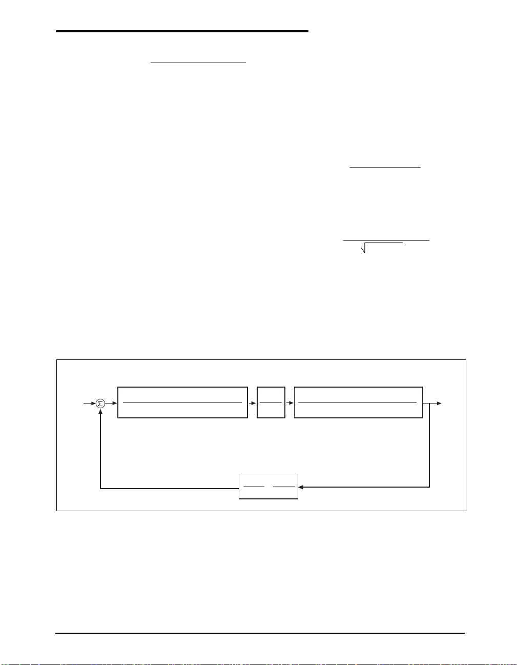
Type III Voltage Loop
Compensation
G
(s) Gain Block
AMP
V
REF
(Volts)
+
_
Notes: R
Condition: Cz2 >> Cp1 & R1 >> Rz3
Output Load Resistance >> R
(SRz2Cz2+1)(SR1Cz3+1) (SR
SR1Cz2(SRz3Cz3+1)(SRz2Cp1+1)
= Output Capacitor Equivalent Series Resistance.
ESR
R
= Output Inductor DC Resistance.
DC
= SP6132 Internal RAMP Amplitude Peak to Peak Voltage.
V
RAMP_PP
& R
ESR
DC
V
FBK
(Volts)
SP7650 Voltage Mode Control Loop with Loop Dynamic
Definitions:
R
= Output Capacitor Equivalent Series Resistance
ESR
R
= Output Inductor DC Resistance
DC
R
RAMP_PP
= SP7650 internal RAMP Amplitude Peak to Peak Voltage
Conditions:
C
2 >> Cp1 and R1 >> Rz3
Z
Output Load Resistance >> R
Date: 2/18/05 SP7650 Wide Input Voltage Range 3A, 300kHz, Buck Regulator © Copyright 2005 Sipex Corporation
ESR
and R
DC
PWM Stage
Gain
G
PWM
Block
V
IN
V
RAMP_PP
Voltage Feedback
G
Gain Block
FBK
R
2
or
(R
)
R
1
+
2
Output Stage
G
(s) Gain
OUT
Block
+ 1)
ESRCOUT
+S(R
) C
[S^2LC
OUT
ESR+RDC
V
REF
V
OUT
+1]
OUT
V
OUT
(Volts)
9
Page 10
Gain
(dB)
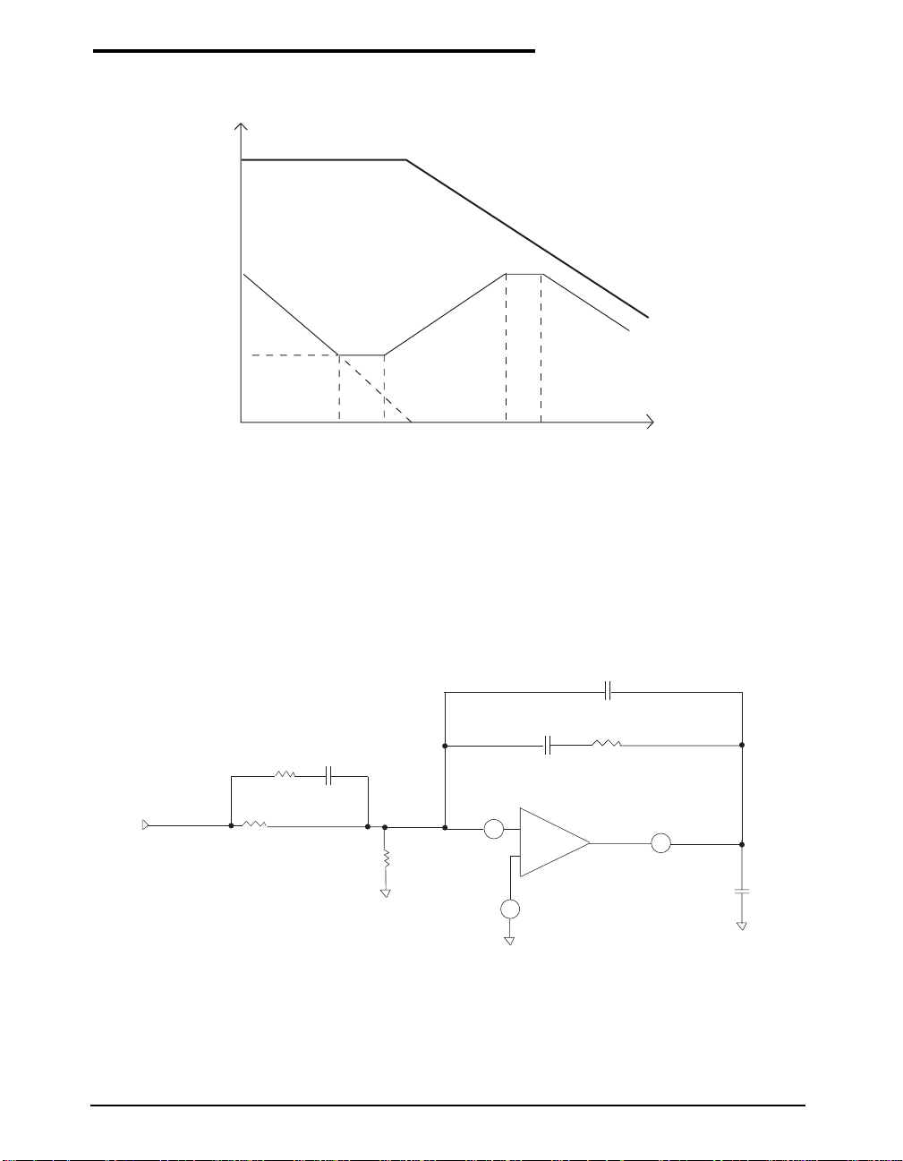
20 Log (RZ2/R1)
Condition:
C22 >> CP1, R1 >> RZ3
1/6.28 (R1) (CZ3)
1/6.28(R22) (CZ2)
1/6.28 (R1) (CZ2)
1/6.28 (RZ2) (CP1)
APPLICATIONS INFORMATION
Error Amplifier Gain
Bandwidth Product
Frequency
(Hz)
1/6.28 (RZ3) (CZ3)
Bode Plot of Type III Error Amplifier Compensation.
V
OUT
RZ3
CZ3
R1
68.1k, 1%
R
SET
Type III Error Amplifier Compensation Circuit
R
SET
=54.48/ (V
OUT
-0.8)
(kΩ)
5
VFB
-
+
+
-
CZ2
0.8V
CP1
RZ2
6
COMP
CF1
Date: 2/18/05 SP7650 Wide Input Voltage Range 3A, 300kHz, Buck Regulator © Copyright 2005 Sipex Corporation
10
Page 11
TYPICAL PERFORMANCE CHARACTERISTICS
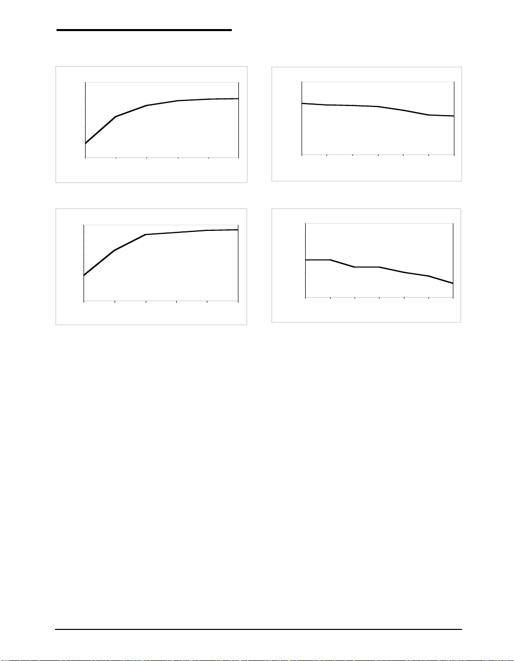
SP7650 Effi. v.s Iout Plots @
95.0
90.0
85.0
80.0
Efficiency (%)
75.0
70.0
0.5 1.0 1.5 2.0 2.5 3.0
94.0
92.0
90.0
88.0
86.0
84.0
82.0
80.0
Efficiency (%)
78.0
76.0
74.0
0.5 1.0 1.5 2.0 2.5 3.0
Vin=12V, and Vout=3.3V
Load Current (A)
SP7650 Effi. v.s Iout Plots @
Vin=12V, and Vout=5.0V
Load Current (A)
SP7650 Vout v.s Iout Plots @
3.34
3.33
3.32
3.31
Output Voltage (V)
3.3
00.51.01.5 2.0 2.5 3.0
4.9710
4.9700
4.9690
4.9680
4.9670
Output Voltage (V)
4.9660
4.9650
0 0.5 1.0 1.5 2.0 2.5 3.0
Vin=12V, and Vout=3.3V
Load Current (A)
SP7650 Vout v.s Iout Plots @
Vin=12V, and Vout=5.0V
Load Current (A)
Date: 2/18/05 SP7650 Wide Input Voltage Range 3A, 300kHz, Buck Regulator © Copyright 2005 Sipex Corporation
11
Page 12
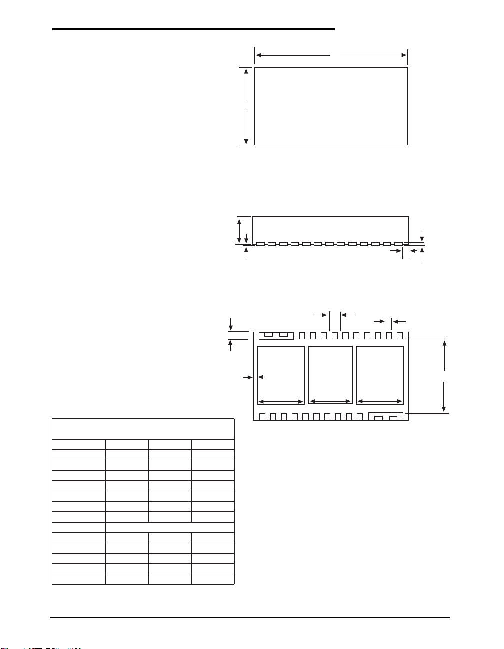
PACKAGE: 26 PIN DFN
D
E
(7 x 4 mm)
Top View
A
A3
A1
L
J
Side View
e
K
b
E2
D2
SYMBOL
26 Pin DFN
MIN NOM MAX
D2
D3
Bottom View
A 0.800 0.850 0.900
A1 0.000 - 0.050
A3 0.178 0.203 0.228
b 0.170 0.220 0.270
D 6.950 7.000 7.050
D2 2.000 2.050 2.100
D3 1.780 1.830 1.880
e
0.500 BSC
E 3.950 4.000 4.050
E2 2.730 2.780 2.830
K 0.340 0.390 0.440
J 0.200 0.250 0.300
L 0.350 0.400 0.450
Note: Dimensions in (mm)
Date: 2/18/05 SP7650 Wide Input Voltage Range 3A, 300kHz, Buck Regulator © Copyright 2005 Sipex Corporation
12
Page 13
ORDERING INFORMATION
Part Number Temperature Package
SP7650ER/TR ......................................... -40°C to +85°C ................................. 26 Pin 7 X 4 DFN
SP7650ER-L/TR .....................................-40°C to +85°C ............. (Lead Free) 26 Pin 7 X 4 DFN
/TR = Tape and Reel
Pack quantity is 3,000 DFN.
CLICK HERE TO ORDER SAMPLES
Corporation
ANALOG EXCELLENCE
Sipex Corporation
Headquarters and
Sales Office
233 South Hillview Drive
Milpitas, CA 95035
TEL: (408) 934-7500
FAX: (408) 935-7600
Sipex Corporation reserves the right to make changes to any products described herein. Sipex does not assume any liability arising out of the
application or use of any product or circuit described herein; neither does it convey any license under its patent rights nor the rights of others.
Date: 2/18/05 SP7650 Wide Input Voltage Range 3A, 300kHz, Buck Regulator © Copyright 2005 Sipex Corporation
13
 Loading...