

Page 1
TVS Diode Arrays (SPA
V+
IN
IN
IN
IN
V+
RoHS
GREEN
®
Diodes)
General Purpose ESD Protection - SP721 Series
SP721 Series 3pF 4kV Diode Array
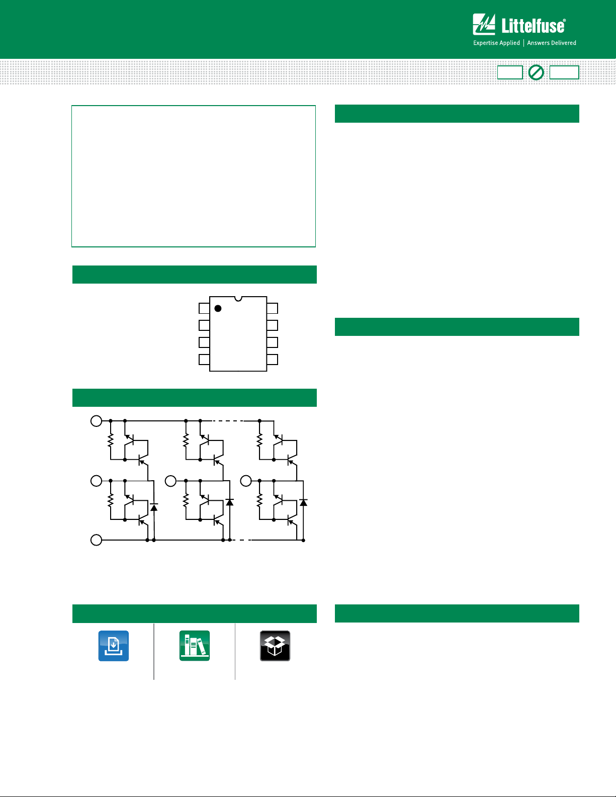
Pinout
SP721 (PDIP, SOIC)
TOP VIEW
Functional Block Diagram
8
1
4
V-
2
IN
1
2
3
V-
4
3, 5-7
IN
8
7
6
5
Pb
Description
The SP721 is an array of SCR/Diode bipolar structures for
ESD and over-voltage protection to sensitive input circuits.
The SP721 has 2 protection SCR/Diode device structures
per input. There are a total of 6 available inputs that can be
used to protect up to 6 external signal or bus lines. Overvoltage protection is from the IN (Pins 1 - 3 and Pins 5 - 7)
to V+ or V-.
The SCR structures are designed for fast triggering at a
threshold of one +V
a -V
diode threshold below V- (Pin 4). From an IN input,
BE
a clamp to V+ is activated if a transient pulse causes the
input to be increased to a voltage level greater than one
V
above V+. A similar clamp to V- is activated if a negative
BE
pulse, one V
less than V-, is applied to an IN input.
BE
Standard ESD Human Body Model (HBM) Capability is:
IN
IN
IN
Features
• ESD Interface Capability for HBM Standards
- MIL STD 3015.7 ................................................. 15kV
- IEC 61000-4-2, Direct Discharge,
- Single Input .......................................... 4kV (Level 2)
- Two Inputs in Parallel ............................ 8kV (Level 4)
- IEC 61000-4-2, Air Discharge ...............15kV (Level 4)
• High Peak Current Capability
- IEC 61000-4-5 (8/20µs) ....................................... ±3A
- Single Pulse, 100µs Pulse Width ........................ ±2A
- Single Pulse, 4µs Pulse Width ............................ ±5A
• Designed to Provide Over-Voltage Protection
- Single-Ended Voltage Range to ........................ +30V
- Differential Voltage Range to ............................ ±15V
• Fast Switching .............................................2ns Rise Time
• Low Input Leakages ............................1nA at 25ºC Typical
• Low Input Capacitance .....................................3pF Typical
• An Array of 6 SCR/Diode Pairs
• Operating Temperature Range....................-40ºC to 105ºC
diode threshold above V+ (Pin 8) or
BE
Additional Information
Datasheet
© 2013 Littelfuse, Inc.
Specifications are subject to change without notice.
Revised: 04/24/13
Resources
Samples
Applications
• Microprocessor/Logic
Input Protection
• Data Bus Protection
• Analog Device Input
Protection
• Voltage Clamp
Page 2
TVS Diode Arrays (SPA
®
Diodes)
General Purpose ESD Protection - SP721 Series
Absolute Maximum Ratings
Parameter Rating Units
Continuous Supply Voltage, (V+) - (V-) +35 V
Forward Peak Current, IIN to VCC, IIN to GND
(Refer to Figure 5)
CAUTION: Stresses above those listed in “Absolute Maximum Ratings” may cause
permanent damage to the device. This is a stress only rating and operation of the device
at these or any other conditions above those indicated in the operational sections of this
specification is not implied.
Note:
ESD Ratings and Capability (Figure 1, Table 1)
Load Dump and Reverse Batter y (Note 2)
Electrical Characteristics T
= -40oC to 105oC, V
A
±2, 100µs A
= 0.5VCC , Unless Otherwise Specified
IN
Thermal Information
Parameter Rating Units
Thermal Resistance (Typical, Note 1) θ
PDIP Package 160
SOIC Package 170
Maximum Storage Temperature Range -65 to 150oC
Maximum Junction Temperature (Plastic
Package)
Maximum Lead Temperature
(Soldering 20-40s)(SOIC Lead Tips Only)
is measured with the component mounted on an evaluation PC board in free air.
1. θ
JA
JA
150
260
o
C/W
o
C/W
o
C/W
o
C
o
C
Parameter Symbol Test Conditions Min Typ Max Units
Operating Voltage Range, V
= [(V+) - (V-)]
V
SUPPLY
SUPPLY
- 2 to 30 - V
Forward Voltage Drop
IN to V- V
IN to V+ V
Input Leakage Current I
Quiescent Supply Current I
QUIESCENT
FWDL
FWDH
IN
IIN = 1A (Peak Pulse) - 2 - V
- 2 - V
-20 5 +20 nA
- 50 200 nA
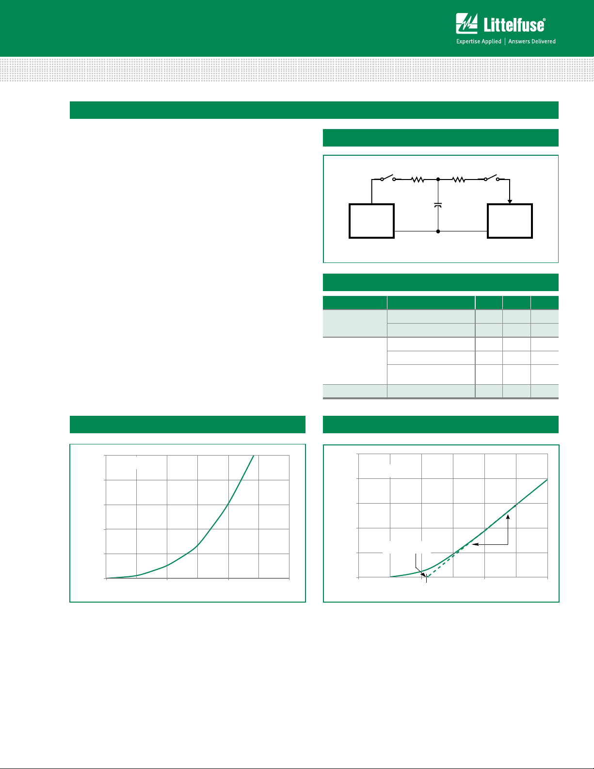
Equivalent SCR ON Threshold Note 3 - 1.1 - V
Equivalent SCR ON Resistance V
Input Capacitance C
Input Switching Speed t
Notes:
2. In automotive and battery operated systems, the power supply lines should be externally protected for load dump and reverse battery. When the V+ and V- Pins are connected to het same
supply voltage source as the device or control line under protection, a current limiti ng resistor should be connected in series between the external supply and the SP721 supply pins to
limit reverse battery current to within the rated maximum limits. Bypass capacitors of typically 0.01µF or larger romf the V+ and V- Pins to ground are recommended.
3. Refer to the Figure 3 graph for definitions of equivalent “SCR ON Threshold” and “SCR ON Resistance”. These characteristics are given here for thumb-rule nformation to determine peak
current and dissipation under EOS conditions.
IN
ON
; Note 3 - 1 - Ω
FWD/IFWD
- 3 - pF
- 2 - ns
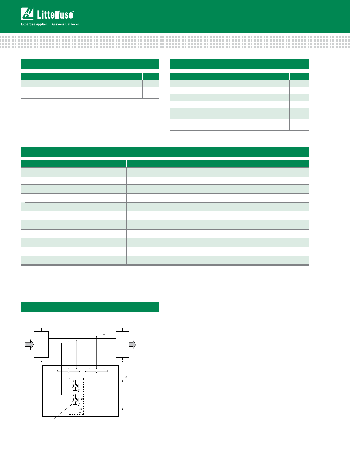
Typical Application of the SP721
(Application as an Input Clamp for Over-voltage, Greater
than 1VBE Above V+ or less than -1VBE below V-)
LINEAR OR
DIGITAL IC
INTERFACE
TO +V
V+
V-
+V
CC
CC
+V
CC
INPUT
DRIVERS
OR
SIGNAL
SOURCES
SP721
SP721 INPUT PROTECTION CIRCUIT (1 OF 6 SHO WN)
IN 5 - 7IN 1 - 3
Specifications are subject to change without notice.
© 2013 Littelfuse, Inc.
Revised: 04/24/13
Page 3
TVS Diode Arrays (SPA
R
2.5
2
1.5
1
0.5
0
V
FWD
I
FWD
EQUIV. SAT. ON
THRESHOLD ~ 1.1V
0
1
2
3
FORWARD SCR CURRENT (A)
FORWARD SCT VOLTAGE DROP (V)
TA = 25ºC
SINGLE PULSE
®
Diodes)
General Purpose ESD Protection - SP721 Series
ESD Capability
ESD capability is dependent on the application and defined
test standard.The evaluation results for various test
standards and methods based on Figure 1 are shown in
Table 1.
For the “Modified”MIL-STD-3015.7 condition that is defined
as an “in-circuit” method of ESD testing, the V+ and V- pins
have a return path to ground and the SP721 ESD capability
is typically greater than 15kV from 100pF through 1.5kΩ.By
strict definition of MIL-STD-3015.7 using “pin-to-pin”device
testing, the ESD voltage capability is greater than 6kV.The
MIL-STD-3015.7 results were determined from AT&T ESD
Test Lab measurements.
The HBM capability to the IEC 61000-4-2 standard is
greater than 15kV for air discharge (Level 4) and greater
than 4kV for direct discharge (Level 2).Dual pin capability (2
adjacent pins in parallel) is well in excess of 8kV (Level 4).
For ESD testing of the SP721 to EIAJ IC121 Machine
Model (MM) standard, the results are typically better than
1kV from 200pF with no series resistance.
Figure 1: Electrostatic Discharge Test
H.V.
SUPPLY
V
D
R
1
CHARGE
SWITCH
IEC 1000-4-2: R150 to 100M
MIL-STD-3015.7: R11 to 10M
C
D
D
DISCHARGE
SWITCH
IN
DUT
Table 1: ESD Test Conditions
Standard Type/Mode R
MIL STD 3015.7
Modified HBM 1.5kΩ 100pF 15kV
Standard HBM 1.5kΩ 100pF 6kV
HBM, Air Discharge 330Ω 150pF 15kV
IEC 61000-4-2
HBM, Direct Discharge 330Ω 150pF 4kV
HBM, Direct Discharge,
Two Parallel Input Pins
330Ω 150pF 8kV
EIAJ IC121 Machine Model 0kΩ 200pF 1kV
C
D
±V
D
D
100
TA = 25ºC
SINGLE PULSE
80
60
40
20
FORWARD SCR CURRENT (mA)
0
600
800
FORWARD SCR VOLTA GE DROP (mV)
© 2013 Littelfuse, Inc.
Specifications are subject to change without notice.
Revised: 04/24/13
1000
Figure 3: High Current SCR Forward Voltage Drop CurveFigure 2: Low Current SCR Forward Voltage Drop Curve
FORWARD SCR CURRENT (A)
1200
2.5
2
1.5
1
0.5
0
TA = 25ºC
SINGLE PULSE
0
EQUIV. SAT. ON
THRESHOLD ~ 1.1V
1
FORWARD SCT VOLTAGE DROP (V)
I
FWD
V
FWD
2
3
Page 4
TVS Diode Arrays (SPA
R
V
C1 ~ 100 µF
General Purpose ESD Protection - SP721 Series
Peak Transient Current Capability of the SP721
®
Diodes)
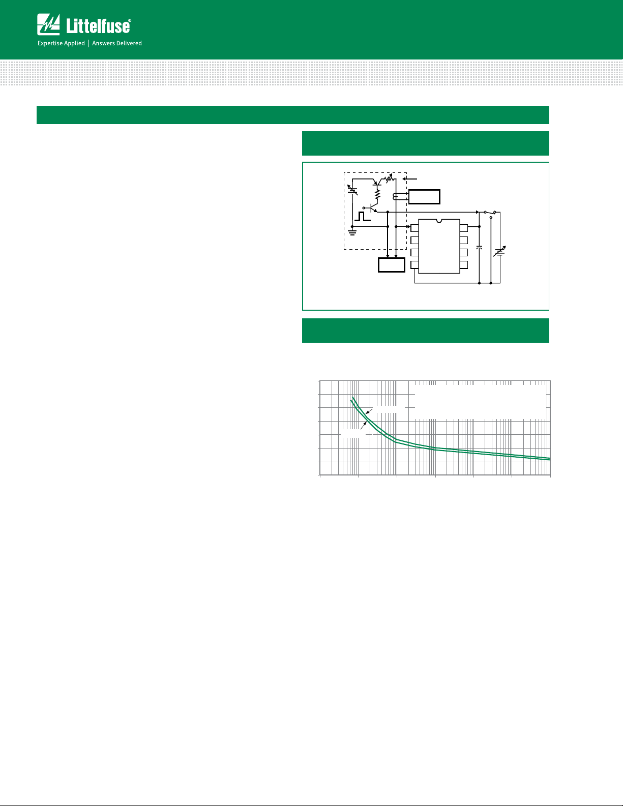
The peak transient current capability rises sharply as the
width of the current pulse narrows. Destructive testing
was done to fully evaluate the SP721’s ability to withstand
a wide range of peak current pulses vs time. The circuit
used to generate current pulses is shown in Figure 4.
The test circuit of Figure 4 is shown with a positive pulse
input. For a negative pulse input, the (-) current pulse input
goes to an SP721 ‘IN’ input pin and the (+) current pulse
input goes to the SP721 V- pin. The V+ to V- supply of the
SP721 must be allowed to float. (i.e., It is not tied to the
ground reference of the current pulse generator.) Figure
5 shows the point of overstress as defined by increased
leakage in excess of the data sheet published limits.
The maximum peak input current capability is dependent
on the ambient temperature, improving as the temperature
is reduced. Peak current curves are shown for ambient
temperatures of 25ºC and 105ºC and a 15V power supply
condition. The safe operating range of the transient peak
current should be limited to no more than 75% of the
measured overstress level for any given pulse width as
shown in the curves of Figure 5.
Note that adjacent input pins of the SP721 may be
paralleled to improve current (and ESD) capability. The
sustained peak current capability is increased to nearly
twice that of a single pin.
Figure 4: Typical SP721 Peak Current Test Circuit
with a Variable Pulse Width Input
VARIABLE TIME DURATION
+
V
X
-
VOLTAG E
~ 10 TYPICAL
1
ADJ. 10V/A TYPICAL
X
PROBE
CURRENT PULSE GENERATO R
R
1
CURRENT
SENSE
(+)
1
IN
2
IN
3
IN
4
V-
SP721
(-)
8
V+
7
IN
6
IN
5
IN
+
C1
-
Figure 5: SP721 Typical Single Peak Current Pulse
Capability
Showing the Measured Point of Overstress in Amperes vs
pulse width time in milliseconds
7
6
5
4
T
3
2
PEAK CURRENT (A)
1
0
0.001 0.01 0.1 1 10
= 105°C
A
T
A
= 25°C
CAUTION: SAFE OPERATING CONDITIONS LIMIT
THE MAXIMUM PEAK CURRENT FOR A GIVEN
PULSE WIDTH TO BE NO GREATER THAN 75%
OF THE VALUES SHOWN ON EACH CURVE.
V+ TO V-SUPPLY = 15V
PULSE WIDTH TIME (ms)
100 1000
Specifications are subject to change without notice.
© 2013 Littelfuse, Inc.
Revised: 04/24/13
Page 5
TVS Diode Arrays (SPA
t
R
R
o
C
e
T
®
Diodes)
General Purpose ESD Protection - SP721 Series
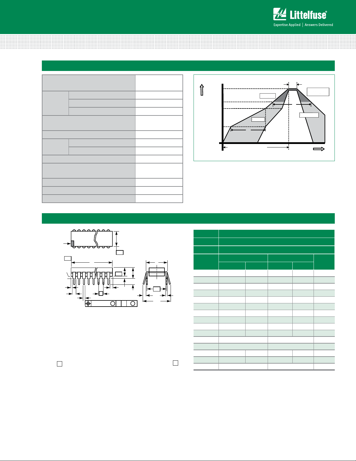
Soldering Parameters
Reflow Condition Pb – Free assembly
Pre Heat
- Temperature Min (T
- Temperature Max (T
) 150°C
s(min)
) 200°C
s(max)
- Time (min to max) (ts) 60 – 180 secs
Average ramp up rate (Liquidus) Temp
(T
) to peak
L
to TL - Ramp-up Rate 5°C/second max
T
S(max)
Reflow
- Temperature (TL) (Liquidus) 217°C
- Temperature (tL) 60 – 150 seconds
Peak Temperature (TP) 260
Time within 5°C of actual peak
Temperature (t
)
p
5°C/second max
+0/-5
°C
20 – 40 seconds
Ramp-down Rate 5°C/second max
Time 25°C to peak Temperature (T
) 8 minutes Max.
P
Do not exceed 260°C
Package Dimensions — Dual-In-Line Plastic Packages (PDIP)
N
INDEX
AREA
PLANE
SEATING
PLANE
Notes:
1. Controlling Dimensions: INCH. In case of conflict between English and Metric
dimensions, the inch dimensions control.
2. Dimensioning and tolerancing per ANSI Y14.5M-1982.
3. Symbols are defined in the “MO Series Symbol List” in Section 2.2 of Publication No.
95.
4. Dimensions A, A1 and L are measured with the package seated in JEDEC seating plane
gauge GS-3.
5. D, D1, and E1 dimensions do not include mold flash or protrusions. Mold flash or
protrusions shall not exceed 0.010 inch (0.25mm).
6. E and e
7. e
and eC are measured at the lead tips with the leads unconstrained. eC must be zero
B
or greater.
8. B1 maximum dimensions do not include dambar protrusions. Dambar protrusions shall
not exceed 0.010 inch (0.25mm).
9. N is t he maximum number of terminal positions.
10. Corner leads (1, N, N/2 and N/2 + 1) for E8.3, E16.3, E18.3, E28.3, E42.6 will have a B1
dimension of 0.030 - 0.045 inch (0.76 - 1.14mm).
12 3 N/2
-A-
BASE
D1
B1
are measured with the leads constrained to be perpendicular to datum -C- .
A
D
B
0.010 (0.25) CAM BS
E1
-B-
E
A2
-C-
D1
e
A
L
A
1
e
C
C
L
e
A
C
e
B
t
T
P
Ramp-up
t
amp-up
PreheatPrehea
S
T
L
T
S(max)
Temperature
T
S(min)
25
time to peak temperature
P
t
L
Ramp-down
Critical Zone
T
amp-d
Time
ritical Zon
L to TP
to
Package PDIP
Pins 8 Lead Dual-in-Line
JEDEC MS-001
Millimeters Inches
Min Max Min Max
A - 5.33 - 0.210 4
A1 0.39 - 0.015 - 4
A2 2.93 4.95 0.115 0.195 -
B 0.356 0.558 0.014 0.022 -
B1 1.15 1.77 0.045 0.070 8, 10
C 0.204 0.355 0.008 0.014 -
D 9.01 10.16 0.355 0.400 5
D1 0.13 - 0.005 - 5
E 7.62 8.25 0.300 0.325 6
E1 6.10 7. 11 0.240 0.280 5
e 2.54 BSC 0.100 BSC -
e
A
e
B
7.62 BSC 0.300 BSC 6
- 10.92 - 0.430 7
L 2.93 3.81 0.115 0.150 4
N 8 8 9
Notes
© 2013 Littelfuse, Inc.
Specifications are subject to change without notice.
Revised: 04/24/13
Page 6
TVS Diode Arrays (SPA
General Purpose ESD Protection - SP721 Series
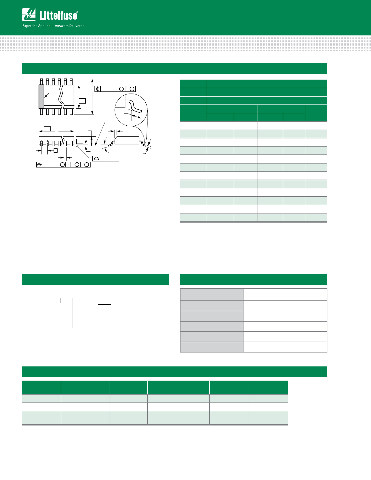
Package Dimensions — Small Outline Plastic Packages (SOIC)
®
Diodes)
N
INDEX
AREA
123
-AD
e
B
0.25(0.010)CAM BS
Notes:
1. Symbols are defined in the “MO Series Symbol List” in Section 2.2 of Publication
Number 95.
2. Dimensioning and tolerancing per ANSI Y14.5M-1982.
3. Dimension “D” does not include mold flash, protrusions or gate burrs. Mold flash,
protrusion and gate burrs shall not exceed 0.15mm (0.006 inch) per side.
4. Dimension “E” does not include interlead flash or protrusions. Inter-lead flash and
protrusions shall not exceed 0.25mm (0.010 inch) per side.
5. The chamfer on the body is optional. If it is not present, a visual index feature must be
located within the crosshatched area.
6. “L” is the length of terminal for soldering to a substrate.
7. “N” is the number of terminal positions.
8. Terminal numbers are shown for reference only.
9. The lead width “B”, as measured 0.36mm (0.014 inch) or greater above the seating
plane, shall not exceed a maximum value of 0.61mm (0.024 inch).
10. Controlling dimension: MILLIMETER. Converted inch dimensions are not necessarily
exact.
E
-B-
SEATING PLANE
-C-
M
H
A
A1
0.25(0.010)BM M
L
h x 45
μ
0.10(0.004)
o
C
Package SOIC
Pins 8
JEDEC MS-012
Millimeters Inches
Min Max Min Max
A 1.35 1.75 0.0532 0.0688 -
A1 0.10 0.25 0.0040 0.0098 -
B 0.33 0.51 0.013 0.020 9
C 0.19 0.25 0.0075 0.0098 -
D 4.80 5.00 0.1890 0.1968 3
E 3.80 4.00 0.1497 0.1574 4
e 1.27 BSC 0.050 BSC -
H 5.80 6.20 0.2284 0.2440 -
h 0.25 0.50 0.0099 0.0196 5
L 0.40 1.27 0.016 0.050 6
N 8 8 7
µ 0º 8º 0º 8º -
Notes
Part Numbering System
SP 721
TVS Diode Arrays
®
(SPA
Diodes)
Series
**
**
G = Green
P = Lead Free
TG= Tape and Reel
Package
AB = 8 Ld SOIC
AP = 8 Ld PDIP
Product Characteristics
Lead Plating Matte Tin
Lead Material Copper Alloy
Lead Coplanarity 0.004 inches (0.102mm)
Substitute Material Silicon
Body Material Molded Epoxy
Flammability UL 94 V-0
Ordering Information
Part Number Temp. Range (ºC) Package
SP721APP -40 to 105 8 Ld PDIP Lead-free SP721AP(P)
SP721ABG -40 to 105 8 Ld SOIC Green SP721A(B)G
SP721ABTG -40 to 105
Notes:
1. SP721AP(P) means device marking either SP721AP or SP721APP.
2. SP721A(B)G means device marking either SP721AG or SP721ABG which are good for types SP721ABG and SP721ABTG.
8 Ld SOIC Tape
and Reel
Environmental
Informaton
Green SP721A(B)G
Marking Min. Order
1
2
2
2000
1960
2500
Specifications are subject to change without notice.
© 2013 Littelfuse, Inc.
Revised: 04/24/13
 Loading...