

Page 1
®
Advanced
SP6656
High Efficiency 400mA Synchronous Buc k Regulator with
Dynamically Adjustable Voltage Output
FEATURES
■ 98% Efficiency Possible
■ Offered in small 2.4 x 2.5mm DFN
■ Ultra-low 20µA Quiescent Current
■ 625mA Inductor Peak Current Limit
P
VIN
OVSO
OVSI
VIN
EN
1
2
3
4
5
SP6656
10 Pin DFN
10
LX
P
9
GND
GND
8
7
V
OUT
6
FB
■ Guaranteed Minimum 400mA Output
Current
■ 2.7V to 5.5V Input Voltage Range
■ Output Adjustable Down to 1.0V
■ 100% Duty Ratio Low Dropout
Operation
■ 80µA Light Load Quiescent Current in
Dropout
■ Dynamic Adjustable Output Voltage
■ Ideal for portable designs powered with
Now Available in Lead Free Packaging
APPLICATIONS
■ Cell Phones
■ PDA's
■ DSC's
■ MP3 Players
■ USB Devices
■ Point of Use Power
Li Ion battery
DESCRIPTION
The SP6656 is a 400mA synchronous buck regulator that is ideal for portable applications that
use a Li-Ion or 3 cell alkaline/NiCD/NiMH input. The SP6656’s proprietary control loop, 20µA light
load quiescent current, and 0.3Ω power switches provide excellent efficiency across a wide range
of output currents. As the input battery supply decreases towards the output voltage the SP6656
seamlessly transitions into 100% duty ratio operation further extending useful battery life. The
SP6656 is protected against overload and short circuit conditions with a precise inductor peak
current limit. Other features include externally programmable output voltage down to 1.0V,
dynamically adjustable output voltage, logic level shutdown control, and 140°C over temperature
shutdown.
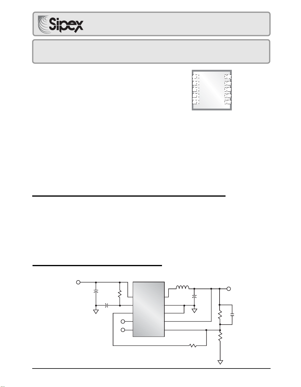
TYPICAL APPLICATION SCHEMATIC
2.7V to 5.5V Input
VI
C
IN
10µF
Date: 02/02/05 SP6656, 400mA Synchronous Buck Regulator with Dynamically Adjustable Voltage Output © Copyright 2005 Sipex Corporation
CV
1µF
10Ω
R
IN
VIN
SP6656
P
VIN
V
IN
OVSO
OVSI
EN
P
GND
GND
V
OUT
LX
FB
3.2 x 1.6 x 1.8mm
L1
10µH
R
S
C
OUT
10µF
R
F
R
I
V
OUT
400mA
VO
CF
22pF
1
Page 2
ABSOLUTE MAXIMUM RATINGS
PVIN,VIN.............................................................................................. 6V
All other pins .............................................................. -0.3V to V
PVIN, P
, LX current ........................................................................ 2A
GND
Storage Temperature .................................................. -65 °C to 150 °C
Operating Temperature ................................................. -40°C to +85°C
+0.3V
IN
These are stress ratings only and functional operation of the device at
these ratings or any other above those indicated in the operation sections
of the specifications below is not implied. Exposure to absolute maximum
rating conditions for extended periods of time may affect reliability.
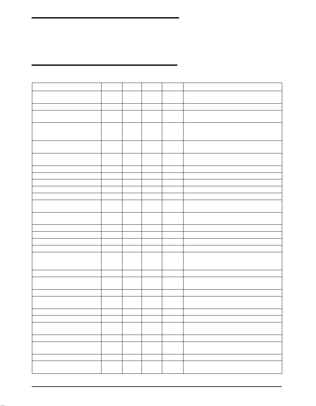
ELECTRICAL CHARACTERISTICS
V
= UV
= V
IN
= 3.6V, V
IN
EN
noted.
PARAMETER MIN TYP MAX UNITS CONDITIONS
Input Voltage Operating 2.7 5.5 V Result of IQ measurement at VIN=PVIN=5.5V
Range
Minimum Output Voltage 1.0 V
FB Set Voltage, Vr 0.784 0.800 0.816 V 25°C, IO = 200mA Close Loop. LI = 10µH,
Overall Accuracy Measured at V
(-40°C to 85°C) ±5%VIN=3.6V, 200mA load, Close Loop
(0°C to 70°C) ±4
On-Time Constant - K
Min, TON=KON/(VIN-V
OUT
Off-Time Constant - K
Min, T
OFF=KOFF/VOUT
Off-Time Blanking 100 ns
Turn On Time 200 400 µs 400mA Load
PMOS Switch Resistance 0.3 0.6 Ω I
NMOS Switch Resistance 0.3 0.6 Ω I
Inductor Current Limit 500 625 750 mA VFB = 0.5V
Power Efficiency 96 % V
Minimum Guaranteed Load 400 500 mA
Current
V
Quiescent Current 20 30 µAV
IN
V
Shutdown Current 1 500 nA EN = 0V
IN
V
Quiescent Current 2 5 µAV
OUT
V
Shutdown Current 1 500 nA EN = 0V
OUT
UVLO
Undervoltage Lockout 2.55 2.70 2.85 V EN = VIN,
Threshold, V
IN
falling
UVLO hysteresis 40 mV
OVSO Output Voltage TBD V
= VFB, IO = 0mA, T
OUT
ON
)
OFF
= -40°C to +85°C, typical values at 27°C unless otherwise
AMB
C
= 22µF
OUT
1.5 2.25 3.0 V*µs Close Loop, LI = 10µH,C
= 5.5V, no load and
IN
= 22µF
OUT
1.6 2.4 3.2 V*µs Inductor current limit tripped, VFB = 0.5V
92 V
Measured at V
= 200mA
PMOS
= 200mA
NMOS
= 2.5V, IO = 200mA
OUT
= 3.3V, IO = 400mA
OUT
= 3.3V, V
OUT
= 3.3V
OUT
= 1V
OUT
= 3.6V and V
IN
= 5.5V
IN
OVSOLeakage Current TBD µA
Over-Temperature 140 °C
Rising Trip Point
Over-Temperature Hysteresis 14 °C
EN Leakage Current 1 500 nA
EN Input Threshold Voltage 0.60 0.90 V High to Low Transition
1.25 1.8 V Low to High Transition
FB Leakage Current 1 100 nA FB =1V
LX Leakage 3 5 µA EN = 0V, V
LX = 0V, LX = V
= 3.6V
IN
+ 0.2V
IN
OVSI Leakage Current 1 500 nA
OVSI Input Threshold Voltage 0.60 0.90 V High to Low Transition
1.25 1.8 Low to High Transition
Date: 02/02/05 SP6656, 400mA Synchronous Buck Regulator with Dynamically Adjustable Voltage Output © Copyright 2005 Sipex Corporation
2
Page 3
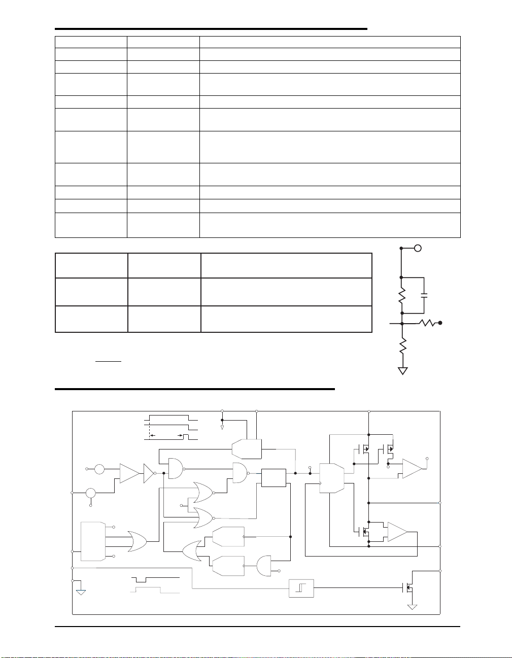
PIN DESCRIPTION
PIN NUMBER PIN NAME DESCRIPTION
1P
2V
VIN
IN
Input voltage power pin. Inductor charging current passes through this pin.
Internal supply voltage. Control circuitry powered from this pin.
3 OVSO Output Voltage Selection Output. OVSI = 1 pulls this node to
GND, OVSI = 0, this node is open.
4 OVSI Output Voltage Select Input. See table 1 for definition.
5ENEN = 1, device is enabled. EN = 0, All internal circuitry is disabled and
power switches are opened.
6FBExternal feedback network input connection. Connect a resistor from
FB to ground and FB to V
regulates to the internal bandgap reference voltage of 0.8V.
7V
OUT
Output voltage sense pin. Used by the timing circuit to set minimum on
to set the output voltage. This pin
OUT
and off times.
8 GND Internal ground pin. Control circuitry returns current to this pin.
9P
GND
Power ground pin. Synchronous rectifier current returns through this pin.
10 LX Inductor switching node. Inductor tied between this pin and the output
capacitor to create regulated output voltage.
V
OUT
ISVOOSVOegatloVtuptuO
R(8.0=
0nepOV
WOL_TUO
IR+F
)R/
I
VO
CF
R
22pF
F
1DNGottrohSV
Table 1. Output Voltage Selection
RI R
+-
V
RAMP
DRVON
Ref
Block
RI +R
Vos
RST
S
REF'
FB'
UVLO
TSD
DRVON
BLANK
BLANK = T
S
DRVON
VOLOW
T
ONOVER
VOLOW
+
-
REF
ILIM/M
MIN Ton
C
(=100ns) or T
BLANK
Note: RA =
REF
+-
FB
EN
OVSI
GND
OVR_I
BLANK
HGIH_TUO
(8.0=RAR+F)R/
A
FB
OVSO
R
S
R
I
FUNCTIONAL DIAGRAM
P
IN
=100ns
T
=
OFF
OFF/VOUT
Min Ton
V
OUT
Min TON =
QR
_
QS
OVR_IK
K
ON
/(
V
-
IN
DRVON
V
)
OUT
DRIVER
V
Internal Supply
T
ONOVER
One-Shot
= K
OFF
OFF/VOUT
VIN
OVR_I
1
M
+
ILIM/M
C
-
LX
+
Zero_X
C
-
P
GND
OVSO
Date: 02/02/05 SP6656, 400mA Synchronous Buck Regulator with Dynamically Adjustable Voltage Output © Copyright 2005 Sipex Corporation
3
Page 4
Refer to the typical application schematic, T
100
95
90
85
80
Efficiency (%)
75
0.1 1.0 10.0 100.0 1000.0
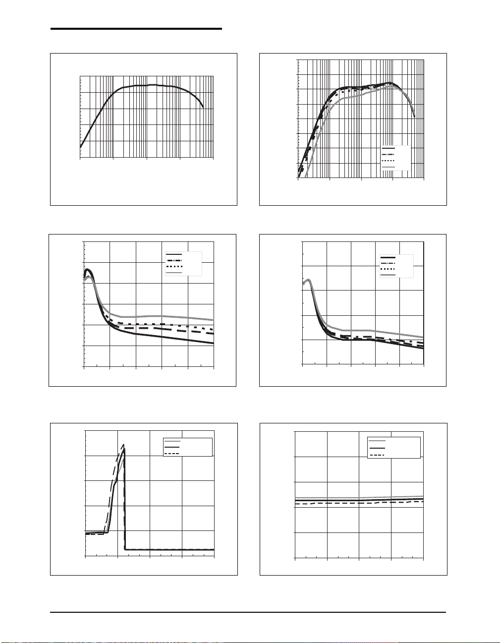
Efficiency vs. Load, V
ILoad (mA)
=3.3V, VIN=3.6V
OUT
TYPICAL PERFORMANCE CHARACTERISTICS
= +27°C
AMB
100
95
90
85
80
75
Efficiency (%)
70
65
60
0.1 1.0 10.0 100.0 1000.0
Efficiency vs Load, V
OUT
ILoad (mA)
= 1.5V
Vi=3.6V
Vi=3.9V
Vi=4.2V
Vi=5.0V
3.45
3.40
3.35
3.30
Vout (V)
3.25
3.20
3.15
0 100 200 300 400 500
Line/Load Rejection, V
500
400
300
Iin (uA)
200
ILoad (mA)
= 3.3V
OUT
Vi=3.6V
Vi=3.9V
Vi=4.2V
Vi=5.0V
Tam b = 85°C
Tam b = 25°C
Tam b = -40°C
1.55
1.53
1.51
Vout (V)
1.49
1.47
1.45
0 100 200 300 400 500
Line/Load Rejection, V
50
40
30
Iin(µA)
20
OUT
ILoad (mA)
= 1.5V
Vi=3.6V
Vi=3.9V
Vi=4.2V
Vi=5.0V
Tamb = 85°C
Tamb = 25°C
Tamb = -40°C
100
0
3.0 3.3 3.6 3.9 4.2
No Load Battery Current, V
Vin (V)
OUT
=3.3V
10
0
3.0 3.3 3.6 3.9 4.2
No Load Battery Current, V
Vin (V)
OUT
=1.5V
Date: 02/02/05 SP6656, 400mA Synchronous Buck Regulator with Dynamically Adjustable Voltage Output © Copyright 2005 Sipex Corporation
4
Page 5
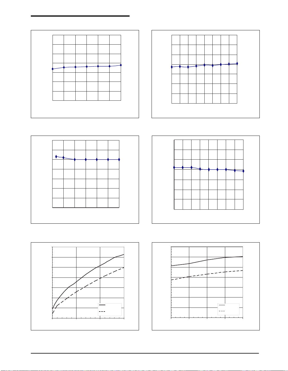
Refer to the typical application schematic, T
TYPICAL PERFORMANCE CHARACTERISTICS
= +27°C
AMB
3.5
3.0
2.5
2.0
1.5
Kon (V*usec)
1.0
0.5
0.0
KON vs VIN, V
3.5
3.0
2.5
2.0
1.5
Koff (V*usec)
1.0
0.5
0.0
3.6 3.9 4.2 4.5 4.8 5.1 5.4
3.6 3.9 4.2 4.5 4.8 5.1 5.4
Vin (V)
=3.3V KON vs VIN, V
OUT
Vin (V)
3.5
3.0
2.5
2.0
1.5
Kon (V*usec)
1.0
0.5
0.0
3.0 3.3 3.6 3.9 4.2 4.5 4.8 5.1 5.4
=1.5V
OUT
3.5
3.0
2.5
2.0
1.5
Koff (V*usec)
1.0
0.5
0.0
3.0 3.3 3.6 3.9 4.2 4.5 4.8 5.1 5.4
Vin (V)
Vin (V)
K
vs VIN, V
OFF
700.0
600.0
500.0
400.0
300.0
Frequency (KHz)
200.0
100.0
Ripple Frequency vs. VIN, I
=3.3V
OUT
Vout = 3.3V
Measured
Vout = 3.3V
=0.4A, V
Calculated
=3.3V
OUT
0.0
3.5 4.0 4.5 5.0
Vin (V)
OUT
K
vs VIN, V
OFF
700.0
600.0
500.0
400.0
300.0
Frequency (KHz)
200.0
100.0
0.0
=1.5V
OUT
3.4 3.8 4.2 4.6 5.0
Ripple Frequency vs. VIN, I
Vin (V)
=0.4A, V
OUT
Vout = 1.5V
Measured
Vout = 1.5V
Calculated
=1.5V
OUT
Date: 02/02/05 SP6656, 400mA Synchronous Buck Regulator with Dynamically Adjustable Voltage Output © Copyright 2005 Sipex Corporation
5
Page 6
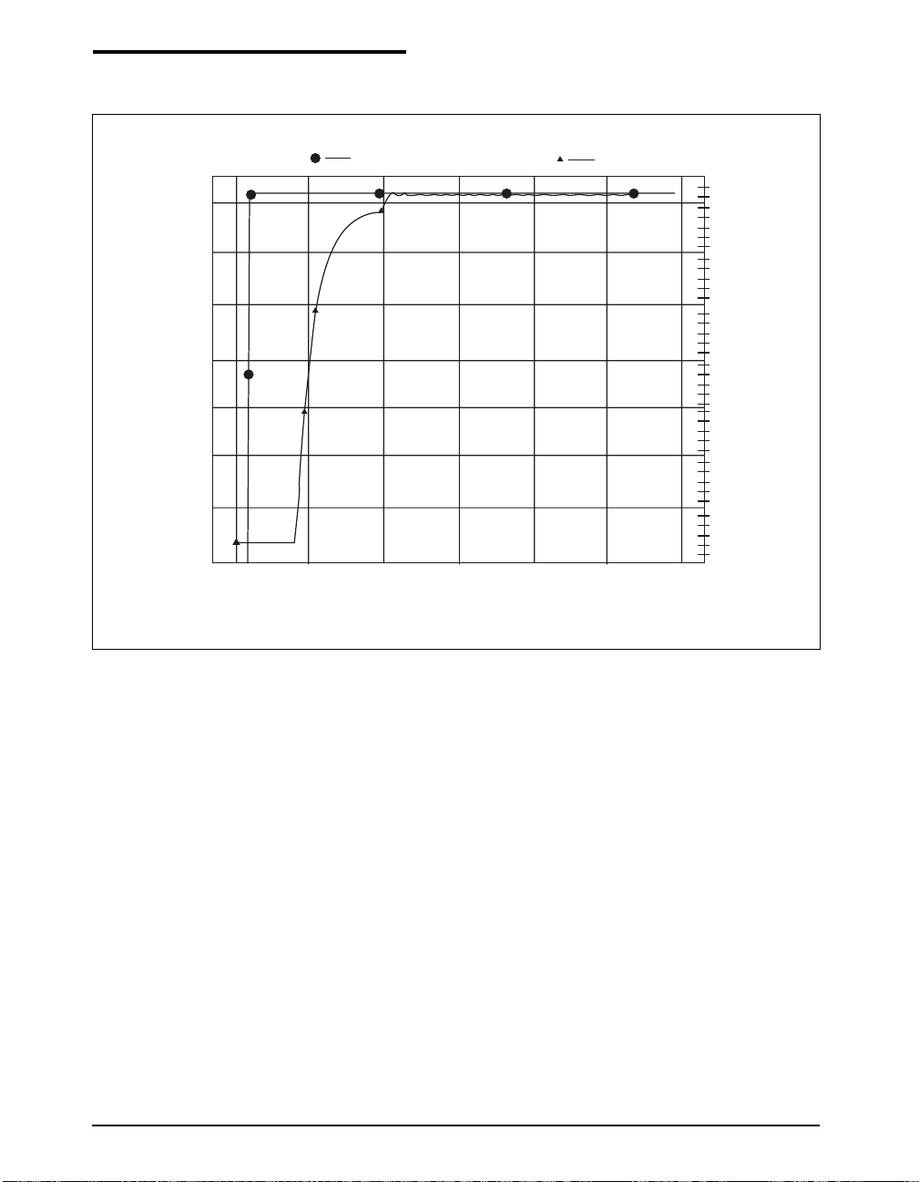
Refer to the typical application schematic, T
1: Startupawg (APU #16)
3.5
TYPICAL PERFORMANCE CHARACTERISTICS
= +27°C
AMB
Plot Overlay
2: S1 Fbx data (APU #10)
0.8
3.0
2.5
2.0
1.5
1.0
1: Awg Pattern (in Volts)
0.5
0.0
Turn on Time, 400mA Load
0.7
2: Digitized Value (in Value)
0.6
0.5
0.4
0.3
0.2
0.1
0.0
0.25 0.50 0.75 1.00 1.25 1.50
Time in Milliseconds
Date: 02/02/05 SP6656, 400mA Synchronous Buck Regulator with Dynamically Adjustable Voltage Output © Copyright 2005 Sipex Corporation
6
Page 7
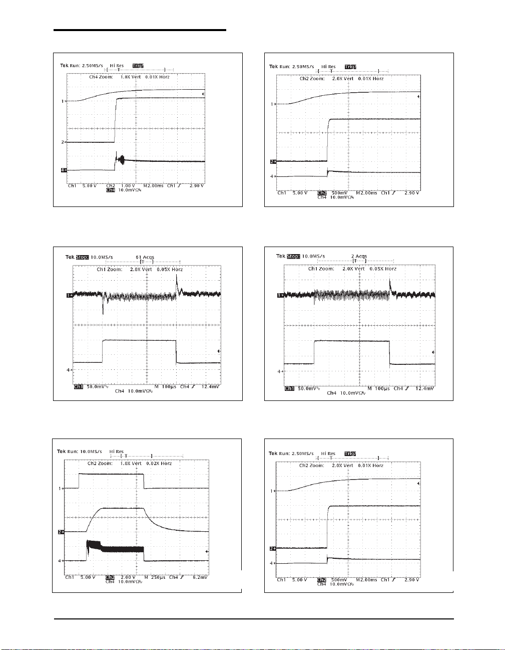
Refer to the typical application schematic, T
CH.1=V
SHDN
5.0V/DIV.
CH.2=V
OUT
2.0V/DIV.
CH.4=I
LX
0.5A/DIV.
TYPICAL PERFORMANCE CHARACTERISTICS
= +27°C
AMB
CH.1=V
IN
5.0V/DIV.
CH.2=V
OUT
0.5V/DIV.
CH.4=I
IN
0.5A/DIV.
VIN Start up, VIN=4.2V, I
Load Step, VIN=4.2V, I
=0.4A, V
OUT
=0.1A to 0.4A, V
OUT
OUT
=3.3V
OUT
=3.3V
CH.1=V
5.0V/DIV.
SHDN
VIN Start up,VIN=4.2V, I
Load Step, VIN=4.2V, I
=0.4A, V
OUT
=0.1A to 0.4A, V
OUT
OUT
=1.5V
OUT
=1.5V
CH.1=V
5.0V/DIV.
SHDN
CH.2=V
Start up from SHDN, VIN=5V ,I
=0.4A, V
OUT
OUT
2.0V/DIV.
CH.4=I
0.5A/DIV.
=3.3V
OUT
LX
Start up from SHDN, VIN=5V, I
=0.4A, V
OUT
OUT
CH.2=V
0.5V/DIV.
CH.4=I
0.5A/DIV.
=1.5V
OUT
LX
Date: 02/02/05 SP6656, 400mA Synchronous Buck Regulator with Dynamically Adjustable Voltage Output © Copyright 2005 Sipex Corporation
7
Page 8
THEORY OF OPERATION
The SP6656 is a high efficiency synchronous
buck regulator with an input voltage range of
+2.7V to +5.5V and an output that is adjustable
between +1.0V and V
. The SP6656 features a
IN
unique on-time control loop that runs in discontinuous conduction mode (DCM) or continuous
conduction mode (CCM) using synchronous
rectification. Other features include over-temperature shutdown, over-current protection, an
external feedback pin, digitally controlled enable and output voltage selection.
The SP6656 operates with a light load quiescent
current of 20µA using a 0.3Ω PMOS main
switch and a 0.3Ω NMOS synchronous switch.
It operates with excellent efficiency across the
entire load range, making it an ideal solution for
battery powered applications and low current
step-down conversions. The part smoothly transitions into a 100% duty cycle under heavy load/
low input voltage conditions.
On-Time Control - Charge Phase
The SP6656 uses a precision comparator and a
minimum on-time to regulate the output voltage
and control the inductor current under normal
load conditions. As the feedback pin drops below the regulation point, the loop comparator
output goes high and closes the main switch.
The minimum on-timer is triggered, setting a
logic high for the duration defined by:
K
TON =
ON
VIN - V
OUT
where:
KON = 2.25V*µsec constant
VIN = VIN pin voltage
V
OUT
= V
pin voltage
OUT
To accommodate the use of ceramic and other
low ESR capacitors, an open loop ramp is added
to the feedback signal to mimic the inductor
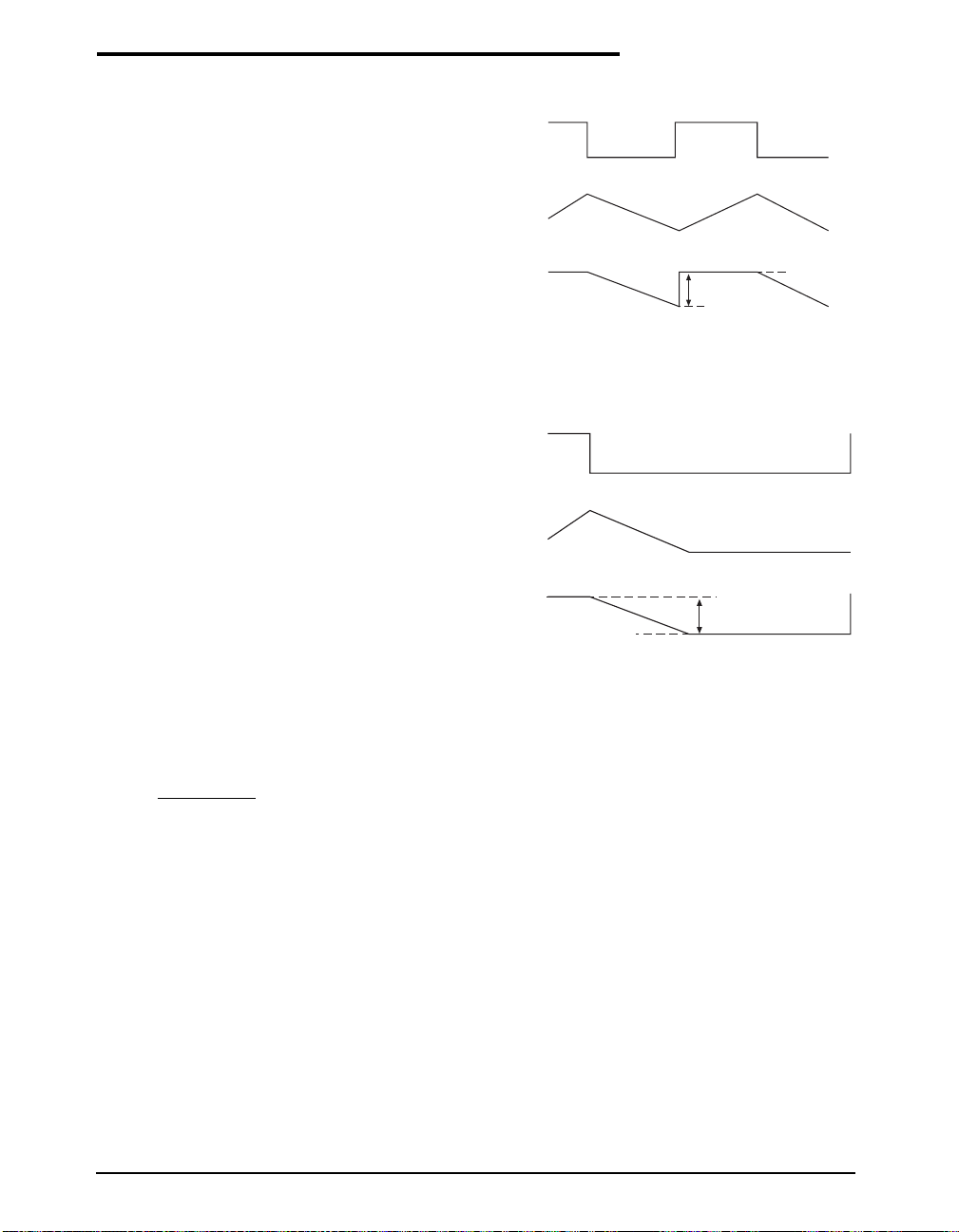
current ripple. The following waveforms describe the ideal ramp operation in both CCM and
DCM operation.
In either CCM or DCM, the negative going
ramp voltage (V
in the functional diagram)
RAMP
RAMP: CCM OPERATION
DRVON
I(L1)
REF, FB
V
FB’
OS
REF’
RAMP: DCM OPERATION
DRVON
I(L1)
FB’
REF’
REF, FB
V
OS
is added to FB and this creates the FB's signal.
This FB signal is applied to the negative terminal of the loop comparator. To the positive
terminal of the loop comparator is applied the
REF voltage of 0.8V plus an offset voltage Vos
to compensate for the DC level of V
RAMP
applied to the negative terminal. The result is an
internal ramp with enough negative going offset
(approximately 50mV) to trip the loop comparator whenever FB falls below regulation.
The output of the loop comparator, a rising
VOLOW, causes a SET if BLANK = 0 and
OVR_I = 0. This starts inductor charging
(DRVON = 1) and starts the minimum on-timer.
The minimum on-timer times out and indicates
DRVON can be reset if the voltage loop is
satisfied. If V
point RESET is held low until V
is still below the regulation
OUT
OUT
is above
Date: 02/02/05 SP6656, 400mA Synchronous Buck Regulator with Dynamically Adjustable Voltage Output © Copyright 2005 Sipex Corporation
8
Page 9

THEORY OF OPERATION
regulation. Once RESET occurs TON minimum
is reset, and the T
one-shot is triggered to
OFF
blank the loop comparator from starting a new
charge cycle for a minimum period. This blanking period occurs during the noisy LX transition
to discharge, where spurious comparator states
may occur. For T
OFF
> T
the loop is in a
BLANK
discharge or wait state until the loop comparator
starts the next charge cycle by DRVON going
high.
If an over current occurs during charge the loop
is interrupted and DRVON is RESET. The offtime one-shot pulse width is widened to T
K
/ V
OFF
, which holds the loop in discharge
OUT
OFF
=
for that time. At the end of the off-time the loop
is released and controlled by VOLOW. In this
manner maximum inductor current is controlled
on a cycle-by-cycle basis. An assertion of UVLO
(undervoltage lockout) or TSD (thermal shutdown) holds the loop in no-charge until the fault
has ended.
On-Time Control - Discharge Phase
The discharge phase follows with the high side
PMOS switch opening and the low side NMOS
switch closing to provide a discharge path for
the inductor current. The decreasing inductor
current and the load current cause the output
voltage to drop. Under normal load conditions
when the inductor current is below the programmed limit, the off-time will continue until
the output voltage falls below the regulation
threshold, which initiates a new charge cycle via
the loop comparator.
The inductor current “floats” in continuous conduction mode. During this mode the inductor
peak current is below the programmed limit and
the valley current is above zero. This is to satisfy
load currents that are greater than half the minimum current ripple. The current ripple, ILR, is
defined by the equation:
≈ KON * VIN - V
I
LR
L VIN - V
OUT
- I
OUT
OUT
* R
CH
where:
L = Inductor value
= Load current
I
OUT
RCH = PMOS on resistance, 0.3Ω typ.
If the I
with (V
* RCH term is negligible compared
OUT
- V
IN
), the above equation simplifies
OUT
to:
K
ILR ≈
L
ON
For most applications, the inductor current ripple
controlled by the SP6656 is constant regardless
of input and output voltage. Because the output
voltage ripple is equal to:
V
(ripple) = I
OUT
LR
* R
ESR
where:
R
= ESR of the output capacitor
ESR
the output ripple of the SP6656 regulator is
independent of the input and output voltages.
For battery powered applications, where the
battery voltage changes significantly, the SP6656
provides constant output voltage ripple throughout the battery lifetime. This greatly simplifies
the LC filter design.
The maximum loop frequency in CCM is defined by the equation:
(VIN - V
FLP ≈
KON * [VIN + I
OUT
) * (V
OUT
+ I
OUT
OUT
(RDC - RCH)]
*
* RDC)
where:
FLP = CCM loop frequency
RDC = NMOS on resistance, 0.3Ω typ.
Ignoring conduction losses simplifies the loop
frequency to:
1 * V
FLP ≈
KON V
OUT
IN
* (VIN - V
OUT
)
AND’ing the loop comparator and the on-timer
reduces the switching frequency for load currents below half the inductor ripple current. This
increases light load efficiency. The minimum
on-time insures that the inductor current ripple
is a minimum of KON/L, more than the load
Date: 02/02/05 SP6656, 400mA Synchronous Buck Regulator with Dynamically Adjustable Voltage Output © Copyright 2005 Sipex Corporation
9
Page 10

THEORY OF OPERATION
current demands. The converter goes in to a
standard pulse frequency modulation (PFM)
mode where the switching frequency is proportional to the load current.
Low Dropout and Load Transient Operation
Using AND logic function the loop comparator
also increases the duty ratio past the ideal D=
V
/V
OUT
up to and including 100%. Under a
IN
light to heavy load transient, the loop comparator will hold the main switch on longer than the
minimum on timer until the output is brought
back into regulation.
Also, as the input voltage supply drops down
close to the output voltage, the main MOSFET
resistance loss will dictate a much higher duty
ratio to regulate the output. Eventually as the
input voltage drops low enough, the output
voltage will follow, causing the loop comparator to hold the converter at 100% duty cycle.
This mode is critical in extending battery life
when the output voltage is at or above the
minimum usable input voltage. The dropout
voltage is the minimum (VIN -V
OUT
) below
which the output regulation cannot be maintained. The dropout voltage of SP6656 is equal
to IL* (0.3Ω+ RL1) where 0.3Ω is the typical
R
of the P-Channel MOSFET and RL is
DS(ON)
the DC resistance of the inductor.
The SP6656 has been designed to operate in
dropout with a light load Iq of only 80µA. The
on-time control circuit seamlessly operates the
converter between CCM, DCM, and low dropout modes without the need for compensation.
The converter’s transient response is quick since
there is no compensated error amplifier in the loop.
Inductor Over-Current Protection
To reduce the light load dropout Iq, the SP6656
over-current system is only enabled when IL1 >
400mA. The inductor over-current protection
circuitry is programmed to limit the peak inductor current to 0.625A. This is done during the
on-time by comparing the source to drain voltage drop of the PMOS passing the inductor
current with a second voltage drop representing
the maximum allowable inductor current. As
the two voltages become equal, the over-current
comparator triggers a minimum off-time one
shot. The off-time one shot forces the loop into
the discharge phase for a minimum T
OFF
time
causing the inductor current to decrease. At the
end of the off-time, loop control is handed back
to the AND logic function on-time signal. If the
output voltage is still low, charging begins until
the output is in regulation or the current limit has
been reached again. During startup and overload conditions, the converter behaves like a
current source at the programmed limit minus
half the current ripple. The minimum T
OFF
is
controlled by the equation:
K
T
OFF (MIN)
Under-Voltage Lockout
=
OFF
V
OUT
The SP6656 is equipped with a programmable
under-voltage lockout to protect the input battery source from excessive currents when substantially discharged. When the input supply is
below the UVLO threshold both power switches
are open to prevent inductor current from flowing. The level of falling input voltage has a
typical hysteresis of 120mV to prevent chattering due to the impedance of the input source.
Under-Current Detection
The synchronous rectifier is comprised of an
inductor discharge switch, a voltage comparator, and a driver latch. During the off-time,
positive inductor current flows into the PGND
pin 9 through the low side NMOS switch to LX
pin 10, through the inductor and the output
capacitor, and back to pin 9. The comparator
monitors the voltage drop across the discharge
NMOS. As the inductor current approaches zero,
the channel voltage sign goes from negative to
positive, causing the comparator to trigger the
driver latch and open the switch to prevent
inductor current reversal. This circuit along
with the on-timer puts the converter into PFM
Date: 02/02/05 SP6656, 400mA Synchronous Buck Regulator with Dynamically Adjustable Voltage Output © Copyright 2005 Sipex Corporation
10
Page 11

THEORY OF OPERATION
mode and improves light load efficiency when
the load current is less than half the inductor
ripple current defined by KON/L.
Thermal Shutdown
The converter will open both power switches if
the die junction temperature rises above 140°C.
The die must cool down below 126°C before the
regulator is re-enabled. This feature protects the
SP6656 and surrounding circuitry from excessive power dissipation due to fault conditions.
Shutdown/Enable Control
The EN pin of the device is a logic level control
pin that shuts down the converter when logic is
low, or enables the converter when logic is high.
When the converter is shut down, the power
switches are opened and all circuit biasing is
extinguished leaving only junction leakage currents on supply pins 1 and 2. After pin 5 is
brought high to enable the converter, there is a
turn on delay to allow the regulator circuitry to
reestablish itself. Power conversion begins with
the assertion of the internal reference ready
signal which occurs approximately 150µs after
the enable signal is received.
Output Voltage Selection
The OVSI (Output Voltage Selection Input) pin
is internally driving a NMOS Gate which Drain
(OVSO pin) is used to short circuit RS and then
achieve a higher output voltage ( see table 1 for
calculation, page 3)
External Feedback Pin
The FB pin 6 is compared to an internal reference voltage of 0.8V to regulate the SP6656
output. The output voltage can be externally
programmed within the range +1.0V to +5.0V
by tying a resistor from FB to ground and FB to
V
(pin7). See the applications section for
OUT
resistor selection information.
APPLICATION INFORMATION
Inductor Selection
The SP6656 uses a specially adapted minimum
on-time control of regulation utilizing a precision comparator and bandgap reference. This
adaptive minimum on-time control has the advantage of setting a constant current ripple for a
given inductor size. From the operations section
it has been shown:
K
ON
L
Inductor Current Ripple, ILR ≈
would be fairly constant for different input and
output voltages, simplifying the selection of components for the SP6656 power circuit. Other
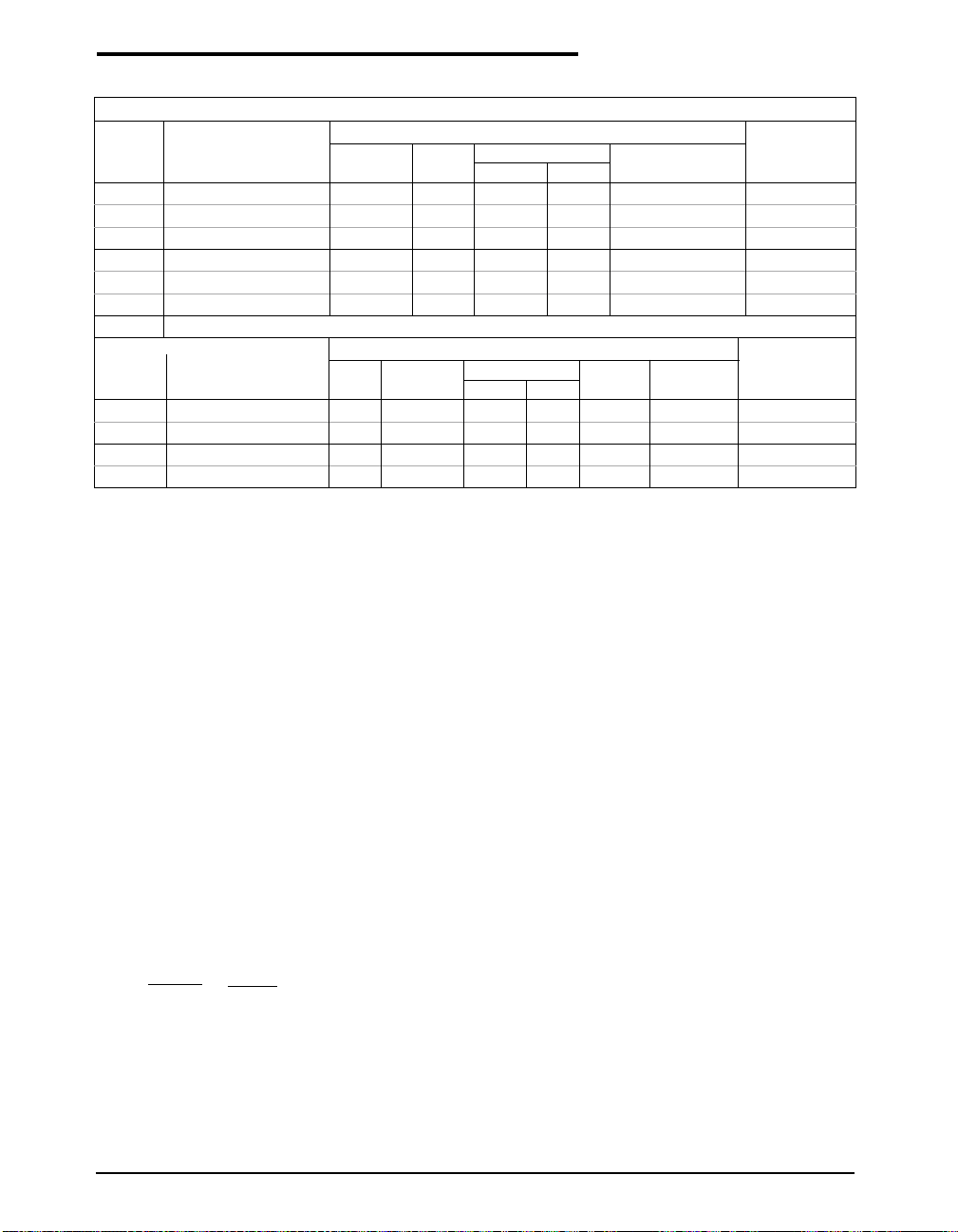
inductor values could be selected, as shown in
Table 2 Components Selection. Using a larger
value than 10µH in an attempt to reduce output
voltage ripple would reduce inductor current ripple
and may not produce as stable an output ripple.
For larger inductors with the SP6656, which has
a peak inductor current of 0.625A, most 15µH
or 22µH inductors would have to be larger
physical sizes, limiting their use in small por-
For the typical SP6656 application circuit with
inductor size of 10µH, and KON of 2V*µsec, the
SP6656 current ripple would be about 200mA, and
Date: 02/02/05 SP6656, 400mA Synchronous Buck Regulator with Dynamically Adjustable Voltage Output © Copyright 2005 Sipex Corporation
table applications. Smaller values like 10µH
would more easily meet the 0.625A limit and
come in small case sizes, and the increased
11
Page 12

APPLICATION INFORMATION
inductor current ripple of almost 200mA would
produce very stable regulation and fast load
transient response at the expense of slightly
reduced efficiency.
Other inductor parameters are important: the inductor current rating and the DC resistance. When
the current through the inductor reaches the level
of I
, the inductance drops to 70% of the
SAT
nominal value. This nonlinear change can cause
stability problems or excessive fluctuation in inductor current ripple. To avoid this, the inductor
should be selected with saturation current at least
equal to the maximum output current of the converter plus half the inductor current ripple. To
provide the best performance in dynamic conditions such as start-up and load transients, inductors
should be chosen with saturation current close to
the SP6656 inductor current limit of 0.625A.
DC resistance, another important inductor characteristic, directly affects the efficiency of the converter, so inductors with minimum DC resistance
should be chosen for high efficiency designs.
Recommended inductors with low DC resistance
are listed in Table 2. Preferred inductors for on
board power supplies with the SP6656 are magnetically shielded types to minimize radiated magnetic field emissions.
Capacitor Selection
The SP6656 has been designed to work with very
low ESR output capacitors (listed in Table 2
Component Selection) which for the typical application circuit are 10µF ceramic capacitors. These
capacitors combine small size, low ESR and good
value. To regulate the output with low ESR capacitors of 0.01Ω or less, an internal ramp voltage
V
has been added to the FB signal to reliably
RAMP
trip the loop comparator (as described in the Operations section).
Output ripple for a buck regulator is determined
mostly by output capacitor ESR, which for the
SP6656 with a constant inductor current ripple can
be expressed as:
V
(ripple) = I
OUT
LR
R
ESR
*
For the 10µF Ceramic Output Capacitor with
0.003Ω ESR, and a 10µH inductor yielding 200mA
inductor current ripple I
, the V
LR
ripple would
OUT
be 0.6mVpp. Since 0.6mV is a very small signal
level, the actual value would probably be as large
as 10mV due to noise and layout issues, but this
illustrates that the SP6656 output ripple can be
very low indeed. To improve stability, a small
ceramic capacitor, C
= 22pF should be paralleled
F
with the feedback voltage divider RF, as shown on
the typical application schematic on page 1. Another function of the output capacitance is to hold
up the output voltage during the load transients and
prevent excessive overshoot and undershoot. The
typical performance characteristics curves show
very good load step transient response for the
SP6656 with the recommended output capacitance of 10µF ceramic.
The input capacitor will reduce the peak current
drawn from the battery, improve efficiency and
significantly reduce high frequency noises induced by a switching power supply. The typical
input capacitor for the SP6656 is 10µF ceramic.
These capacitors will provide good high frequency
bypassing and their low ESR will reduce resistive
losses for higher efficiency. An RC filter is recommended for the VIN pin 2 to effectively reduce the
noise for the ICs analog supply rail which powers
sensitive circuits. This time constant needs to be at
least 5 times greater than the switching period,
which is calculated as 1/FLP during the CCM
mode. The typical application schematic uses the
values of R
= 10Ω and C
VIN
= 1µF to meet these
VIN
requirements.
Date: 02/02/05 SP6656, 400mA Synchronous Buck Regulator with Dynamically Adjustable Voltage Output © Copyright 2005 Sipex Corporation
12
Page 13
APPLICATION INFORMATION
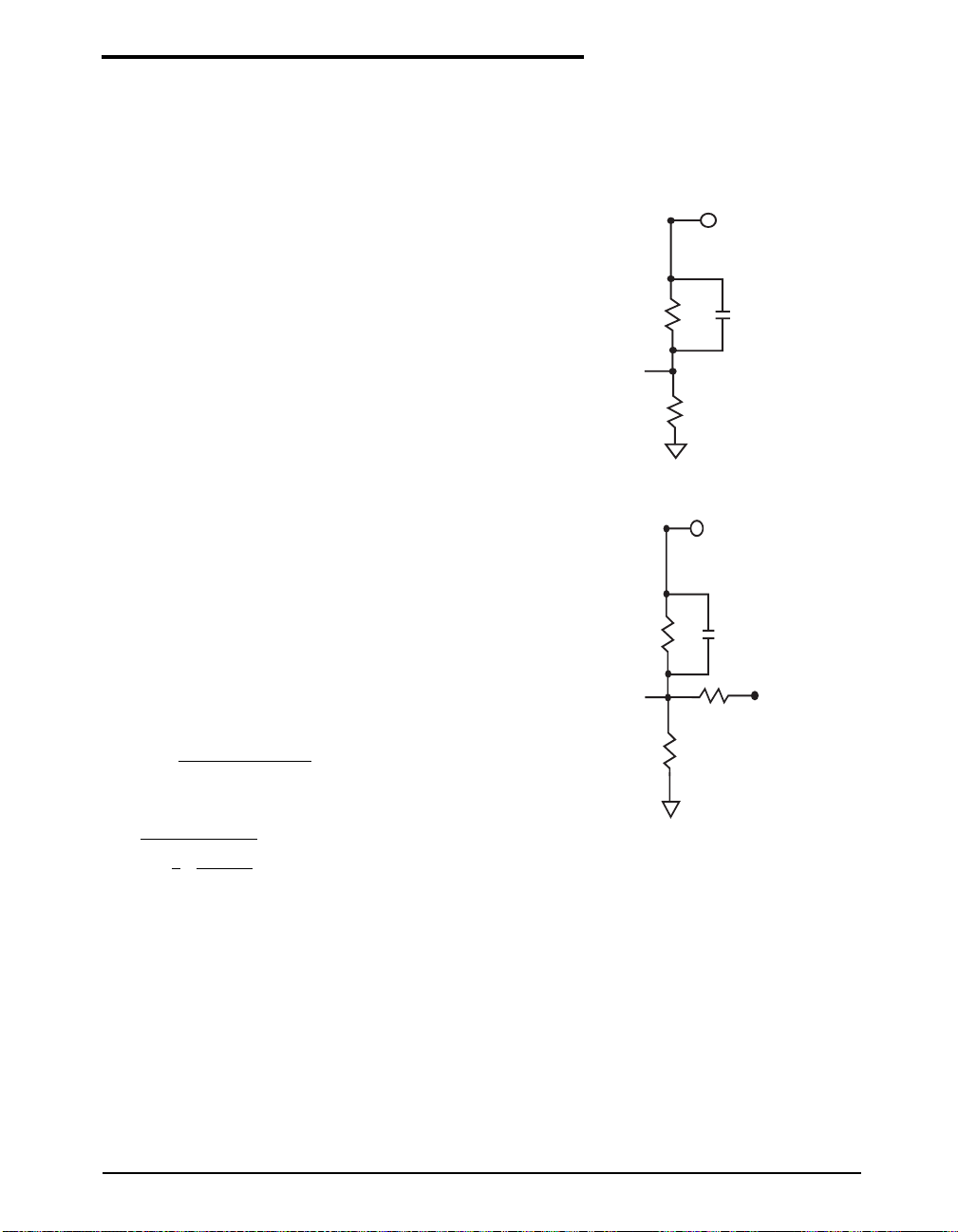
The output voltage is programmed by the external divider, as shown in the typical
application circuit on Page 1. Depending on the topology used, 1 or 2 voltages ,V
is set as follows:
OUT
1) Single V
OUT
First pick a value for RI that is no larger than 300K.
Too large a value of RI will reduce the AC voltage
seen by the loop comparator since the internal FB
pin capacitance can form a low pass filter with RF
in parallel with RI. The formula for RF with a given
RI and output voltage is:
RF = (V
2) Dual V
/ 0.8V - 1) x (RI)
OUT
(selectable)
OUT
First pick the lowest voltage that will be used and
utilize the same method as above.
RF = (V
OUT_LOW
/ 0.8V - 1) x (RI) RI≤ 300k
Then use the following equation to determine R
V
OUT
FB
V
OUT
S:
FB
VO
CF
R
22pF
F
R
I
VO
CF
R
F
22pF
R
OVSO
S
0.8 x R
[RI//RS] =
R
S =
Date: 02/02/05 SP6656, 400mA Synchronous Buck Regulator with Dynamically Adjustable Voltage Output © Copyright 2005 Sipex Corporation
V
OUT_HIGH
[RI//RS]
[RI//RS]
1
F
- 0.8
R
I
R
I
13
Page 14
APPLICATION INFORMATION
INDUCTORS SURFACE MOUNT
Inductor Specification
Inductance Manufacturer/Part No. Series R Ω I
(µH) LxW(mm) Ht. (mm) Website
10 Murata LQH32CN100K11 0.300 0.45 3.2 x 1.6 1.8
10 TDK RLF5018T-100MR94 0.056 0.94 5.6 x 5.2 2.0 Shielded Ferrite Core tdk.com
10 Coilcraft LPO6013-103K 0.300 0.70 6.0 x 5.4 1.3 Unshielded Ferrite Core coilcraft.com
22 Murata LQH32CN220K21 0.710 0.25 3.2 x 1.6 1.8
22 TDK RLF5018T- 220MR63 0.130 0.63 5.6 x 5.2 2.0 Shielded Ferrite Core tdk.com
22 Coilcraft LPO6013-103 0.520 0.45 6.0 x 5.4 1.3 Unshielded Ferrite Core coilcraft.com
CAPACITORS - SURFACE MOUNT
Capacitance Manufacturer/Part No. ESR RippleCurrent Size Voltage Capacitor Type Manufacturer
(µF) Ω (max) (A) @ 45°C LxW(mm) Ht. (mm) (V) Website
10 TDK C2012X5R0J106M 0.003 1.00 2.0 x 1.2 1.25 6.3 X5R Ceramic tdk.com
10
Murata GRM21BR60J106KE01
4.7 TDK C2012X5R0J475M 0.005 1.00 2.0 x 1.2 1.25 6.3 X5R Ceramic tdk.com
4.7
Murata GRM21BR60J475KE01
Note: Components highlighted in bold are those used on the SP6656 Evaluation Board.
Table 2 Component Selection
0.003 1.00 2.0 x 1.2 1.25 6.3 POSCAP murata.com
0.005 1.00 2.0 x 1.2 1.25 6.3 POSCAP murata.com
(A) Size Inductor Type Manufacturer
SAT
Unshielded Ferrite Core
Unshielded Ferrite Core
Capacitor Specification
murata.com
murata.com
Output Voltage Ripple Frequency
An important consideration in a power supply
application is the frequency value of the output
ripple. Given the control technique of the SP6656
(as described in the operations section), the
frequency of the output ripple will vary when in
light to moderate load in the discontinuous or
PFM mode. For moderate to heavy loads greater
than about 100mA inductor current ripple, (for
the typical 10µH inductor application on 100mA
is half the 200mA inductor current ripple), the
output ripple frequency will be fairly constant.
From the operations section, this maximum loop
frequency in continuous conduction mode is:
FLP ≈
1 V
K
ON
OUT
*
(V
- V
OUT
)
IN
*
V
IN
Data for loop frequency, as measured from
output voltage ripple frequency, can be found in
the typical performance curves.
Layout Considerations
Proper layout of the power and control circuits is
necessary in a switching power supply to obtain
good output regulation with stability and a minimum of output noise. The SP6656 application
circuit can be made very small and reside close to
the IC for best performance and solution size, as
long as some layout techniques are taken into
consideration. To avoid excessive interference
between the SP6656 high frequency converter and
the other active components on the board, some
rules should be followed. Refer to the typical
application schematic on page 1 and the sample
PCB layout shown in the following figures to
illustrate how to layout a SP6656 power supply.
Avoid injecting noise into the sensitive part of
circuit via the ground plane. Input and output
capacitors conduct high frequency current through
the ground plane. Separate the control and power
grounds and connect them together at a single
point. Power ground plane is shown in the figure
titled PCB top sample layout and connects the
Date: 02/02/05 SP6656, 400mA Synchronous Buck Regulator with Dynamically Adjustable Voltage Output © Copyright 2005 Sipex Corporation
14
Page 15

APPLICATION INFORMATION
ground of the C
capacitor to the ground of the
OUT
CIN capacitor and then to the PGND pin 10. The
control ground plane connects from pin 9 GND to
ground of the C
capacitor and the RI ground
VIN
return of the feedback resistor. These two separate
control and power ground planes come together in
the figure titled PCB top sample layout where
SP6656 pin 9 GND is connected to pin 10 PGND.
Power loops on the input and output of the converter should be laid out with the shortest and
widest traces possible. The longer and narrower
the trace, the higher the resistance and inductance
it will have. The length of traces in series with the
capacitors increases its ESR and ESL and reduces
their effectiveness at high frequencies. Therefore,
put the 1µF bypass capacitor as close to the V
IN
and
GND pins of the converter as possible, the 10µF
C
close to the P
IN
pin and the 10µF output
VIN
capacitor as close to the inductor as possible. The
external voltage feedback network RF, RI, RS and
feedforward capacitor CF should be placed very
close to the FB pin. Any noise traces like the LX
pin should be kept away from the voltage feedback
network and separated from it by using power
ground copper to minimize EMI.
Date: 02/02/05 SP6656, 400mA Synchronous Buck Regulator with Dynamically Adjustable Voltage Output © Copyright 2005 Sipex Corporation
15
Page 16
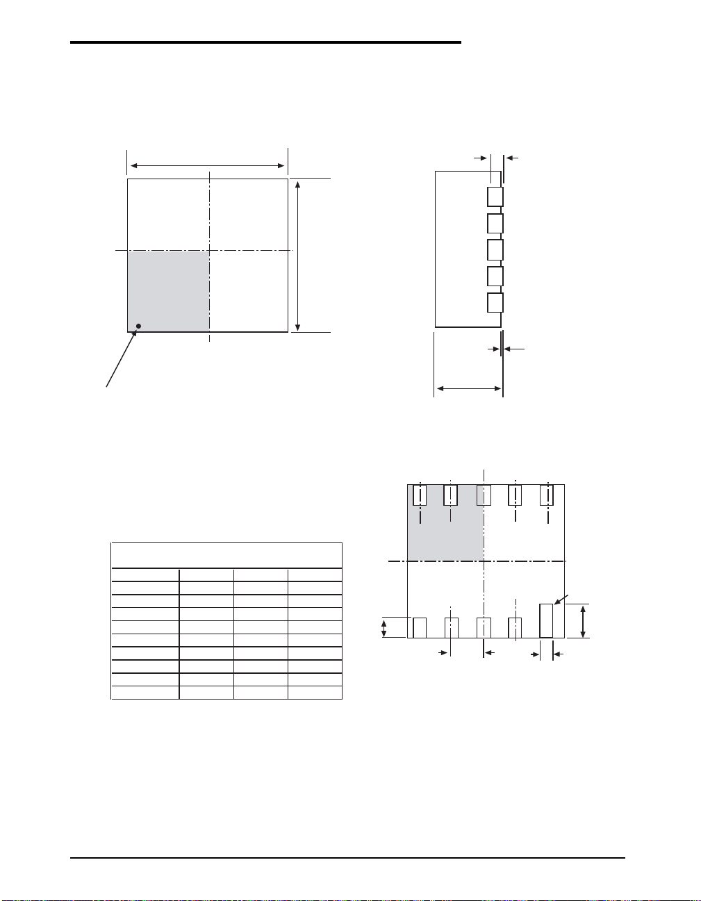
PACKAGE: 10 PIN DFN
Pin 1 Dot by
Marking
SYMBOL
A
B
Top View
2.4x2.5 10 Pin DFN
MIN NOM MAX
A 2.45 2.50 2.55
B 2.35 2.40 2.45
C 0.18 0.20 0.23
D-0.00 0.05
E 0.80 0.85 0.90
F 0.45 0.50 0.55
G 0.45 0.50 0.55
H 0.20 0.25 0.30
I 0.70 0.75 0.80
F
D
E
Side View
G
Bottom View
C
Pin 1
Indentification
I
H
Note: Dimensions in (mm)
Date: 02/02/05 SP6656, 400mA Synchronous Buck Regulator with Dynamically Adjustable Voltage Output © Copyright 2005 Sipex Corporation
16
Page 17
ORDERING INFORMATION
Part Number Operating Temperature Range Package Type
SP6656ER ........... ...............................-40°C to +85°C ............................................................... 10 Pin DFN
SP6656ER/TR .....................................-40°C to +85°C...............................................................10 Pin DFN
Available in lead free packaging. To order add "-L" suffix to part number.
Example: SP6656ER/TR = standard; SP6656ER-L/TR = lead free
/TR = Tape and Reel
Pack quantity is 3,000 for DFN.
Corporation
ANALOG EXCELLENCE
Sipex Corporation
Headquarters and
Sales Office
233 South Hillview Drive
Milpitas, CA 95035
TEL: (408) 934-7500
FAX: (408) 935-7600
Sipex Corporation reserves the right to make changes to any products described herein. Sipex does not assume any liability arising out of the
application or use of any product or circuit described herein; neither does it convey any license under its patent rights nor the rights of others.
Date: 02/02/05 SP6656, 400mA Synchronous Buck Regulator with Dynamically Adjustable Voltage Output © Copyright 2005 Sipex Corporation
17
 Loading...