

Page 1
®
SP6641A/6641B
500mA Alkaline DC/DC Boost Regulator in SOT-23
■ Ultra Low Quiescent Current: 10µA
■ Wide Input Voltage Range: 0.9V to 4.5V
■ 90mA I
■ 500mA I
■ 100mA I
■ 500mA I
at 1.3V Input (SP6641A-3.3V)
OUT
at 2.6V Input (SP6641B-3.3V)
OUT
at 2.0V Input (SP6641A-5.0V)
OUT
at 3.3V Input (SP6641B-5.0V)
OUT
■ Fixed 3.3V or 5.0V Output Voltage
■ Up to 87% Efficiency
■ 0.3Ω NFET RDSon
■ Startup Voltage Guaranteed at 0.9V
■ 0.33A Inductor Current Limit (SP6641A)
■ 1A Inductor Current Limit (SP6641B)
■ Logic Shutdown Control
■ SOT-23-5 Package
APPLICATIONS
■ PDA's
■ DSC's
■ CD/MP3 Players
■ Pagers
■ Digital Cameras
■ Portable Handheld Medical Devices
Now Available in Lead Free Packaging
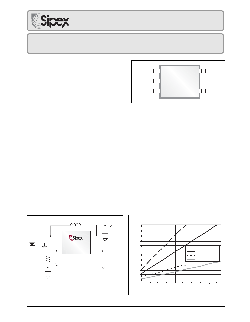
GND
V
OUT
LX
1
5
SP6641
2
5 Pin SOT-23
3
4
V
BATT
SHDN
DESCRIPTION
The SP6641 is an ultra-low quiescent current, high efficiency, DC-DC boost converter designed
for single and dual cell alkaline, or Li-ion battery applications found in PDA’s, MP3 players, and
other handheld portable devices. The SP6641 features a 10µA quiescent current, a 0.3Ω N-
channel charging switch, 0.9V input startup, and a 0.33A or 1.0A inductor current limiting feature.
The SP6641 is offered in a 5 pin SOT-23 package and provides an extremely small power supply
footprint optimized for portable applications. The SP6641 is preset to 3.3V and can be controlled
by a 1nA active LOW shutdown pin.
L1
1
LX
2
D1
R1
C2
SP6641A 3.3V & 5V: C1 = C2 = 22µF Ceramic, L1 = 22µH CDRH5D28,
SP6641B 3.3V & 5V: C1 = C2 = 100µF POSCAP, L1 = 10µH CDRH5D28,
GND
3
V
OUT
C3
D1 = MBR0520, C3 = Open, R1 = Shorted.
D1 = ZHCS2000, C3 = 1µF Ceramic, R1 = 10Ω.
U1
SP6641A
V
BATT
®
®
SHDN
Figure 1. Typical Application Schematic
Rev. 5/26/05,
*Patent Pending
SP6641A/6641B 500mA Alkaline DC/DC Boost Regulator in SOT-23 © Copyright 2002 Sipex Corporation
0.9V to 4.5V
V
BATT
C1
5
4
SHDN
V
OUT
+3.3V or 5V
700
650
600
550
500
450
400
350
(mA)
300
OUT
I
250
200
150
100
50
0
1.0 1.5 2.0 2.5 3.0 3.5 4.0 4.5
V
(V)
IN
SP6641B, 1.0A, 3.3V
SP6641B, 1.0A, 5V
SP6641A, 0.33A, 3.3V
SP6641A, 0.33A, 5V
Figure 2. Maximum Load Current in Operation
1
Page 2
ABSOLUTE MAXIMUM RATINGS
These are stress ratings only and functional
operation of the device at these ratings or any other
above those indicated in the operation sections of
the specifications below is not implied. Exposure to
absolute maximum rating conditions for extended
periods of time may affect reliability.
LX, V
LX Current.......................................................... 1.5A
Reverse V
Storage Temperature ........................ -65°C to 150°C
Operating Temperature..................... -40°C to +85°C
Lead Temperature (Soldering, 10 sec) .......... 300 °C
, SHDN, V
OUT
Current ................................... 220mA
BATT
to GND pin .......-0.3 to 6.0V
BATT
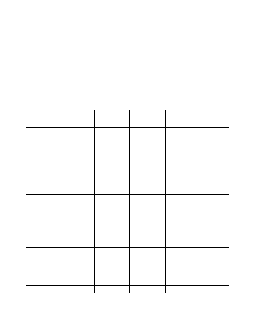
ELECTRICAL SPECIFICATIONS
V
= V
BATT
unless otherwise noted.
PARAMETER MIN TYP MAX UNITS CONDITIONS
Input Voltage Operating Range, 0.5 4.5 V after startup
V
BATT
Startup Voltage, V
Output Voltage, V
Quiescent Current into V
I
Q(OUT)
Quiescent Current into V
I
QB
Shutdown Current into V
I
SHDN
Shutdown Current into V
I
SHDN
Inductor Current Limit 280 330 380 mA
(SP6641A)
Inductor Current Limit 850 1000 1150 mA
(SP6641B)
Output Current (SP6641AEK-3.3) 90 mA V
Output Current (SP6641BEK-3.3) 200 mA V
Output Current (SP6641AEK-5.0) 100 mA V
Output Current (SP6641BEK-5.0) 275 mA V
Minimum Off-Time Constant 1.50 V*µsT
K
OFF
NMOS Switch Resistance 0.3 0.75 Ω Inmos=100mA
SHDN Input Voltage Vil 20 % % of V
SHDN Input Current 1 100 nA
SHDN
= 1.3V, I
= 0mA, -40°C <TA < +85°C, V
LOAD
BATT
OUT
3.16 3.30 3.44 V 3.3V V
4.80 5.00 5.20 V 5.0V V
,1015µAV
OUT
, 250 500 nA V
BATT
,1500 nA V
OUT
,20100 nA V
BATT
Vih 80 % % of V
= +3.3V or +5.0V preset, typical values at 27°C
OUT
0.85 0.90 V R
1.00 V R
190 mA V
500 mA V
175 mA V
500 mA V
LOAD
LOAD
=3.5V, 3.3V V
OUT
V
=5.5V, 5.0V V
OUT
=3.5V, 3.3V V
OUT
V
=5.5V, 5.0V V
OUT
SHDN
SHDN
=1.3V
BATT
=2.6V
BATT
=1.3V
BATT
=2.6V
BATT
=2.0V
BATT
=3.3V
BATT
=2.0V
BATT
=3.3V
BATT
≥ K
OFF
=3kΩ, TA =27°C
=3kΩ,-40°C <TA < +85°C
preset
OUT
preset
OUT
preset
OUT
preset
OUT
preset
OUT
preset
OUT
=0V
=0V
/ (V
OUT
– VIN)
OFF
BATT
BATT
Rev. 5/26/05,
*Patent Pending
SP6641A/6641B 500mA Alkaline DC/DC Boost Regulator in SOT-23 © Copyright 2002 Sipex Corporation
2
Page 3
PIN DESCRIPTION
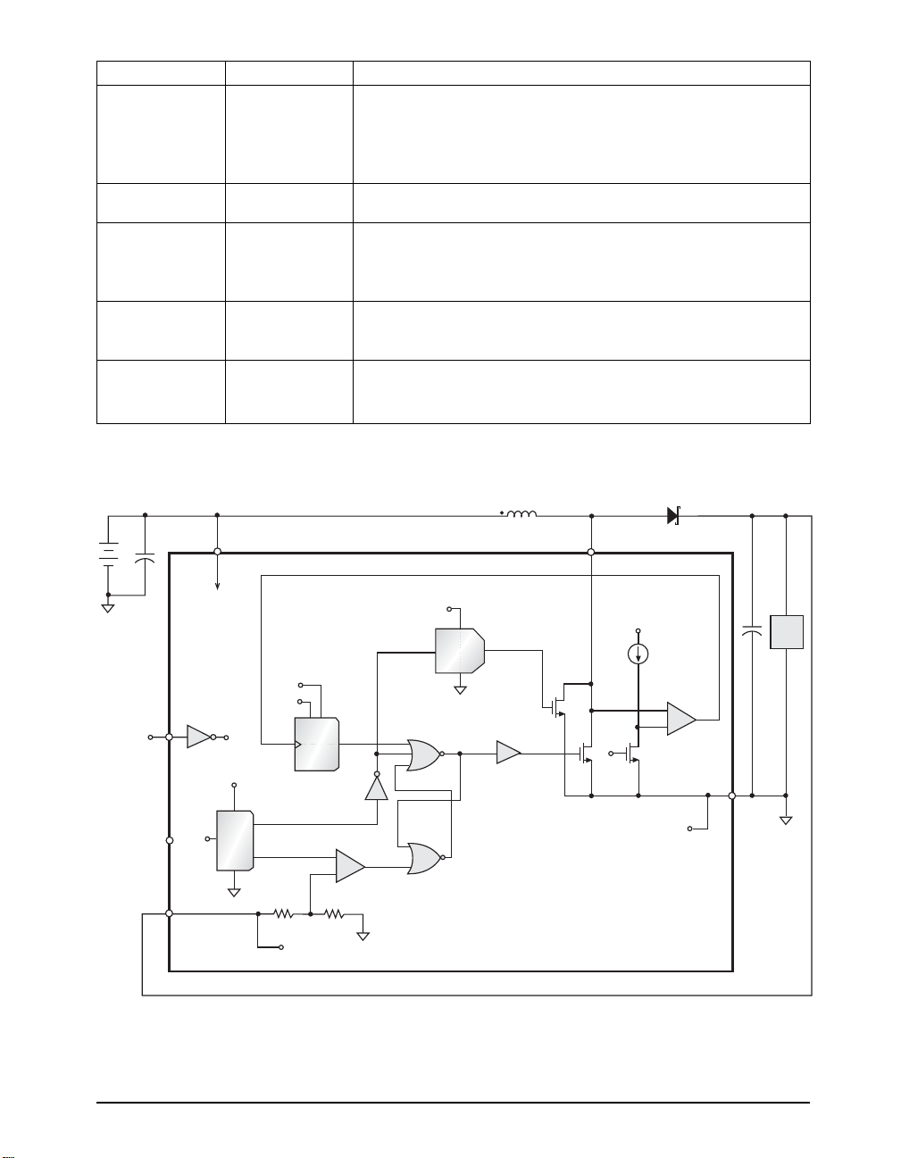
PIN NO. PIN NAME DESCRIPTION
1LXInductor switching node. Connect one terminal of the inductor to the
positive terminal of the battery. Connect the second terminal of the
inductor to this pin. The inductor charging current flows into LX,
through the internal charging N-channel FET, and out through the GND
pin.
2 GND Ground pin. The internal regulator bias currents and the inductor
charging current flows out of this pin.
3V
OUT
Output voltage sense pin, internal regulator voltage supply, and
minimum off-time one shot input. Kelvin connect this pin to the positive
terminal of the output capacitor, but for SP6641B, use 10Ω series
resistor and 1µF bypass per Figure 1 schematic.
4 SHDN Shutdown. Tie this pin to V
ground to disable all circuitry inside the chip. In shutdown mode, the
output voltage will float at a diode drop below the battery potential.
5V
BATT
Battery voltage pin. The startup circuitry runs off of this pin. The
regulating circuitry also uses this voltage to control the minimum offtime. T
BLOCK DIAGRAM
V
BATT
V
BATT
OFF
≥ K
OFF
/ (V
OUT
for normal operation. Tie this pin the
BATT
– VIN).
LX
V
OUT
SHDN
Internal
V
BATT
V
OUT
V
BATT
Min.
SHDN
V
OUT
Ref
SHDN
Block
V
OUT
REFREADY
Internal
Supply
T
OFF
T
OFF
REF
+
V
OUT(LOW)
C
FB
-
V
BATT
SUGATE
SU
EN
OSC
Q
CHARGE
Qn
DRIVER
NGATE
R
S
V
OUT
I
/M
PK
LX
V
OUT
M
1
ITH
+
-
Internal
Ground
ICHN
C
LOAD
GND
SP6641
Rev. 5/26/05,
*Patent Pending
SP6641A/6641B 500mA Alkaline DC/DC Boost Regulator in SOT-23 © Copyright 2002 Sipex Corporation
3
Page 4
PERFORMANCE CHARACTERISTICS
)
)
Refer to the circuit in Figure 1, T
AMB
= +25°C
100
VIN = 3.0V
95
90
V
V
= 2.6V
IN
= 2.0V
IN
V
V
= 1.3V
IN
= 1.0V
IN
85
80
75
Efficiency (%)
70
65
60
0.1 1.0 10.0 100.0 1000.0
Iload (mA)
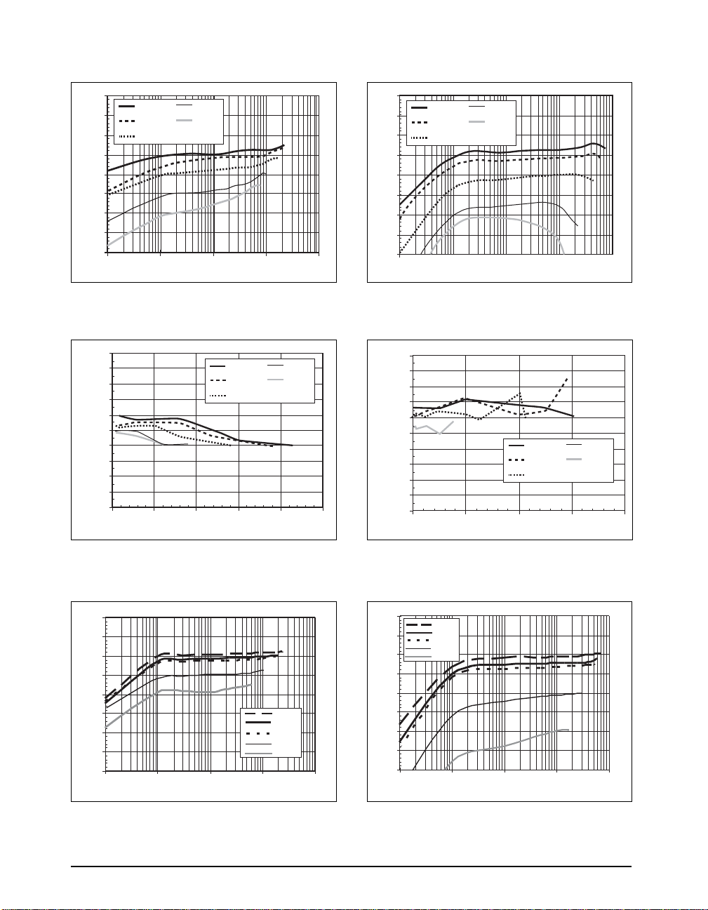
Figure 3. SP6641AEK - 3.3 Efficiency vs Load Current
3.400
3.380
3.360
3.340
VIN = 3.0V
V
= 2.6V
IN
= 2.0V
V
IN
3.320
3.300
OUT
V
3.280
3.260
3.240
3.220
3.200
0
50 100 150
Iload (mA)
= 1.3V
V
IN
V
= 1.0V
IN
200 250
Figure 5. SP6641AEK - 3.3 Line/Load Rejection vs Load
Current
100
V
VIN = 3.0V
95
V
= 2.6V
V
IN
= 2.0V
IN
90
V
= 1.3V
IN
= 1.0V
IN
85
80
75
Efficiency (%)
70
65
60
0.1 1.0 10.0 100.0 1000.0
Iload (mA)
Figure 4. SP6641BEK - 3.3 Efficiency vs Load Current
3.400
3.380
3.360
3.340
3.320
3.300
OUT
V
3.280
3.260
3.240
VIN = 3.0V
V
= 2.6V
IN
= 2.0V
V
IN
V
V
= 1.3V
IN
= 1.0V
IN
3.220
3.200
0 200 400 600 800
Iload (mA)
Figure 6. SP6641BEK - 3.3 Line/Load Rejection vs Load
Current
100
95
90
85
80
75
Efficiency (%)
70
65
60
0.1 1.0 10.0 100.0 1000.0
Iload (mA
Vi=4.2V
Vi=3.6V
Vi=3.3V
Vi=2.0V
Vi=1.3V
Figure 7. SP6641AEK-5.0 Efficiency Vs Load Current
Rev. 5/26/05,
*Patent Pending
SP6641A/6641B 500mA Alkaline DC/DC Boost Regulator in SOT-23 © Copyright 2002 Sipex Corporation
100
95
90
Vi=4.2V
Vi=3.6V
Vi=3.3V
Vi=2.0V
Vi=1.3V
85
80
75
Efficiency (%)
70
65
60
0.1 1.0 10.0 100.0 1000.0
Iload (mA
Figure 8. SP6641BEK-5.0 Efficiency Vs Load Current
4
Page 5
PERFORMANCE CHARACTERISTICS
)
)
)
)
Refer to the circuit in Figure 1, T
= +25°C
AMB
5.200
5.180
5.160
5.140
5.120
5.100
Vo (V)
5.080
5.060
5.040
5.020
5.000
050100 150 200 250
Vi=4.2V
Vi=3.6V
Vi=3.3V
Vi=2.0V
Vi=1.3V
Iload (mA
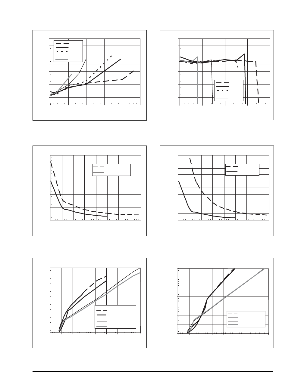
Figure 9. SP6641AEK-5.0 Line/Load Rejection Vs Load
Current
250
200
150
Iin (uA)
100
50
0
0.5 1.0 1.5 2.0 2.5 3.0 3.5 4.0 4.5
SP6641AEK-5.0
SP6641AEK-3.3
Vin (V
5.100
5.080
5.060
5.040
5.020
5.000
Vo (V)
4.980
4.960
4.940
4.920
4.900
0 200 400 600 800
Iload (mA)
Vi=4.2V
Vi=3.6V
Vi=3.3V
Vi=2.0V
Vi=1.3V
Figure 10. SP6641BEK-5.0 Line/Load Rejection Vs
Load Current
500
450
400
350
300
250
Iin (uA)
200
150
100
50
0
0.5 1.0 1.5 2.0 2.5 3.0 3.5 4.0 4.5
Vin (V)
SP6641B-5.0
SP6641B-3.3
Figure 11. SP6641AEK-3.3 & SP6641AEK-5.0 No Load
Battery Current
250
200
150
Io (mA)
100
50
0
0.5 1.0 1.5 2.0 2.5 3.0 3.5 4.0 4.5
SP6641AEK-3.3, 22µH
SP6641AEK-3.3, 10µH
SP6641AEK-5.0, 22µH
SP6641AEK-5.0, 10µH
Vin (V
Figure 13. SP6641AEK-3.3 & SP6641AEK-5.0
Maximum Resistive Load Current in Startup
Rev. 5/26/05,
*Patent Pending
SP6641A/6641B 500mA Alkaline DC/DC Boost Regulator in SOT-23 © Copyright 2002 Sipex Corporation
Figure 12. SP6641BEK-3.3 & SP6641AEK-5.0 No Load
Battery Current
700
600
500
400
Io (mA)
300
200
100
0
0.5 1.0 1.5 2.0 2.5 3.0 3.5 4.0 4.5
Vin (V
SP6641BEK-3.3, 22µH
SP6641BEK-3.3, 10µH
SP6641BEK-5.0, 22µH
SP6641BEK-5.0, 10µH
Figure 14. SP6641BEK-3.3 & SP6641BEK-5.0
Maximum Resistive Load Current in Startup
5
Page 6

OPERATION
General Overview
The SP6641 is a high efficiency, low quiescent
current step-up DC-DC converter ideal for single
and dual cell alkaline and single cell Lithium Ion
battery applications such as medical monitors,
PDA’s, MP3 players, and other portable end
products. The SP6641’s 10µA quiescent current, low 0.3Ω NFET switch, and unique PFM
control scheme combine to provide excellent
efficiency over a wide output power range.
Other features include a logic level enable control pin, guaranteed 0.9V startup, a tiny SOT23
5 pin package, and precise inductor peak current
control. SP6641A sources up to 90mA at 1.3V,
typ. and SP6641B sources up to 500mA at 2.6V,
typ. by supporting different peak inductor current
levels. Only two capacitors, an inductor, and a
diode are required to build a power supply for
the SP6641A. The SP6641B, 1A peak current
requires an additional small resistor and capacitor as a low pass filter for the V
IC power pin.
OUT
Loop Regulation
The SP6641 combines a fixed inductor peak
current limit, a feed-forward minimum off-time
one-shot, and a precision loop comparator to
regulate the output voltage. Under light-load
conditions the loop operates as a standard PFM
converter. The frequency of fixed amplitude
inductor current triangles is modulated to regulate the load. Under heavy load conditions, the
converter adjusts the number of successive continuous mode current pulses to regulate the load.
Refer to the block diagram for the following
explanation of operating modes in loop regulation.
The output voltage is internally divided down and
fed to the negative terminal of the loop comparator. A +1.25V bandgap reference voltage is applied to the positive terminal of the comparator. As
the output voltage droops below the regulation
threshold due to the load the loop comparator
output (signal V
OUT(LOW)
) transitions to a logic
“1”. This sets the SR latch and initiates inductor
charging by pulling the signal NGATE high. Inductor charging continues until the current reaches
the internally programmed limit, at which point,
the off-time one-shot is triggered.
The off-time one-shot via signal T
SR latch regardless of the SET state (V
resets the
OFF
OUT(LOW)
opens the NMOS charge switch, and forces the
inductor to discharge through the rectifying
diode for a minimum time defined by the oneshot duration. The end of the off-time pulse
releases the SR latch, and its output state is once
again determined by the output of the loop
comparator (V
OUT(LOW)
). Under light load conditions, the output voltage will have been pulled
above the regulation threshold during the minimum off-time, the signal V
OUT(LOW)
logic “0”, and the NMOS charging switch will
remain open. The inductor current discharges
until it reaches zero or the loop comparator
triggers a new charge cycle.
Under a heavy load, the output voltage will
remain below the regulation point at the end of
the off-time pulse. In this condition, V
has a logic value of 1 which immediately starts
a new charge/discharge cycle defined by the
peak inductor current and the minimum offtime. The inductor current will remain in a
continuous conduction mode until the loop comparator indicates the output voltage is above the
regulation threshold, and the inductor current
will relax towards zero.
During continuous mode bursts, the inductor
current frequency and ripple amplitude are controlled by the minimum off-time one-shot and
the input and output voltage levels. The SP6641
sets the minimum off-time to:
K
T
OFF
K
V
V
= Off-time Constant, typically 1.5µs*V
OFF
= Output Voltage
OUT
= Input Voltage
IN
Plugging the T
=
OFF
OFF
(V
– VIN), where:
OUT
expression into the boost
mode equations yields the maximum output
current in regulation:
V
IN
OUT
IPK –
) (
I
OUT(MAX)
≈ η (
V
where:
η = Efficiency, typically 0.80 to 0.90
I
= Programmed inductor peak current, typi-
PK
cally 0.33A for the SP6641A, typically
1.0A for the SP6641B.
),
L= Inductor value
K
2L
will be a
OUT(LOW)
OFF
)
Rev. 5/26/05,
*Patent Pending
SP6641A/6641B 500mA Alkaline DC/DC Boost Regulator in SOT-23 © Copyright 2002 Sipex Corporation
6
Page 7
OPERATION
Loop Regulation: continued
The SP6641 feed forward off-time control delivers more load current than constant off-time
control because the input battery voltage drops
during its life cycle. The term (IPK – K
OFF
/2L) is
the average current delivered to the output capacitor during the discharge phase. This is constant with respect to input and output voltage.
With constant off-time control, the average discharge current term becomes
(IPK-T
OFF
*(V
OUT-VIN
)/2L),
which decreases as the input voltage drops.
Table 1 illustrates the average inductor current
delivered to the load during discharge versus the
input voltage. The SP6641 feed forward offtime control and the constant off-time control
are compared. For purposes of illustration, the
off times of each control scheme are normalized
at a typical two cell alkaline input voltage of
2.6V. The values used in Table 1 are:
IPK = 0.33A
L = 22µH
V
= 3.3V
OUT
T
(SP6641) = 1.5V*µs/(3.3-VIN)
OFF
T
(constant) = 2.14µs
OFF
SP6641A Constant T
V
T
IN
OFF
Avg I
T
L
OFF
OFF
Avg I
3.0 5.00µs 0.30A 2.14µs 0.32A
2.6 2.14µs 0.30A 2.14µs 0.30A
2.0 1.15µs 0.30A 2.14µs 0.27A
1.3 0.75µs 0.30A 2.14µs 0.23A
1.0 0.65µs 0.30A 2.14µs 0.22A
Table 1- Average IL vs. Input Voltage
The following equation defines the burst mode
frequency under heavy load conditions:
F
BURST
=
(
OUT
K
– V
OFF
VIN – V
IN
) (
V
+ VD –V
OUT
C
)
C
V
where:
VD = Forward schottky drop, (0.4V, typ)
VC = Average charging switch drop,
Rnmos*IPK, typically 0.1V
Ignoring the conduction losses of VD and VC,
the burst frequency equation simplifies to:
F
BURST
=
(V
OUT
K
– VIN)V
OFFVOUT
Startup
The internal regulator circuitry is bootstrapped
to the V
pin. This requires a low voltage
OUT
oscillator and charging switch powered from the
V
pin to pump up the output voltage until
BATT
the reference is established. The reference provides a REFREADY signal that determines when
output control is handed over to the regulator.
REFREADY shuts down the startup circuit and
enables the regulator when the reference is valid
and V
is above +1.9V. Once the regulator is
OUT
given control it will continue to pump up the
output at full power until regulation is reached.
For two cell alkaline input voltages and above,
the output voltage will be pulled above +1.9V
quickly through the rectifying diode before the
reference has a chance to establish. In this scenario the startup circuit will coarsely regulate
around +2.8V until the REFREADY signal asserts. This keeps the output from overshooting
in startup with higher input voltages.
Startup is guaranteed at +0.9V at room temperature with a 3kΩ load. Heavier loads will require
L
a higher input voltage.
Shutdown/Enable Control
Pin 4 of the device is a V
referred control
BATT
pin that shuts down the converter with the pin
tied to ground, or enables the converter with the
pin tied to V
. When the converter is shut-
BATT
down the power switch is opened and all circuit
biasing is extinguished leaving only junction leakage currents on supply pins 3 and 5. The output
voltage will droop to one diode drop below the
battery voltage through the rectifying diode.
After pin 4 is brought high, the startup circuit is
enabled and starts pumping up the output until
REFREADY hands over control to the internal
regulator.
IN
Rev. 5/26/05,
*Patent Pending
SP6641A/6641B 500mA Alkaline DC/DC Boost Regulator in SOT-23 © Copyright 2002 Sipex Corporation
7
Page 8

APPLICATION INFORMATION
Circuit Layout
Printed circuit board layout is a critical part of a
power supply design. Poor designs can result in
excessive EMI on the voltage gradients and
feedback paths on the ground planes with applications involving high switching frequencies
and large peak currents. Excessive EMI can
result in instability or regulation errors. All
power components should be placed on the PC
board as closely as possible with the traces kept
short, direct, and wide (>50mils or 1.25mm).
Extra copper on the PC board should be integrated into ground as a pseudo-ground plane.
On a multilayer PC board, route the star ground
using component-side copper fill, then connect
it to the internal ground plane using vias. For the
SP6641A/6641B devices, input and output filter capacitors should be soldered with their
ground pins as close together as possible in a
star-ground configuration. The VOUT pin must
be bypassed directly to ground as close to the
SP6641A/6641B devices as possible (within
0.2in or 5mm). The DC-DC converter and any
digital circuitry should be placed on the opposite corner of the PC board as far away from
sensitive RF and analog input stages. Noisy
traces, such as from the LX pin, should be kept
away from the voltage-feedback VOUT node
and separated from it using grounded copper to
minimize EMI. See the SP6641A/6641B Evaluation Board Manual for PC Board Layout design details.
Component Selection
Selection of capacitors, inductors and schottky
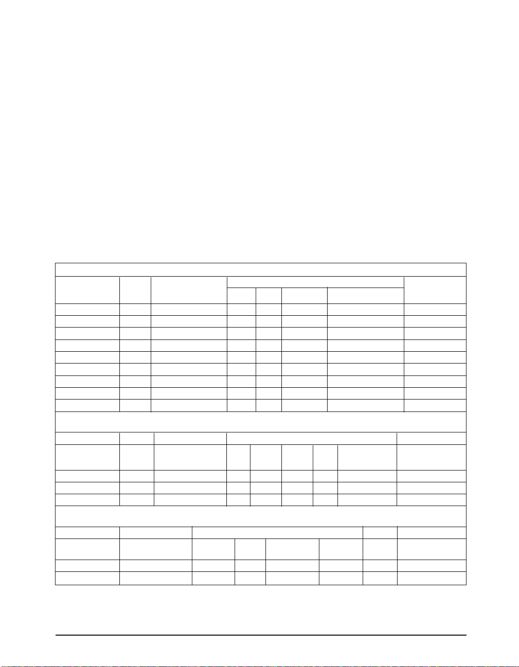
diodes for SP6641A and SP6641B power supply circuits can be made through the use of
Table 1 component selection. Capacitor equivalent series resistance is a major contributor to
output ripple, usually greater than 60%. Low
ESR capacitors are recommended. Ceramic capacitors have the lowest ESR. Low-ESR tantalum capacitors may be a more acceptable solution having both a low ESR and lower cost than
large ceramic capacitors. Designers should select input and output capacitors with a rating
exceeding the peak inductor current. Do not
allow tantalum capacitors to exceed their ripplecurrent ratings. For example, in the SP6641A a
22µF, 6V, low-ESR, surface-mount tantalum
output filter capacitor typically provides 60mV
output ripple when stepping up from 1.3V to
3.3V at 20mA. An input filter capacitor can
reduce peak currents drawn from the battery and
improve efficiency. Low-ESR aluminum electrolytic capacitors are acceptable in some applications but standard aluminum electrolytic capacitors are not recommended.
In selecting an inductor, the saturation current
specified for the inductor needs to be greater
then the SP6641A/B peak current to avoid saturating the inductor, which would result in a loss
in efficiency and could damage the inductor.
The SP6641A evaluation board uses a Sumida
CDRH5D28 22µH inductor with an Isat value
of 0.9A and a DCR of 0.095Ω, which easily
handles the Ipeak of 0.33A of the SP6641A and
will deliver high efficiencies. The SP6641B
evaluation board uses a Sumida CDRH5D28
10µH inductor with an Isat value of 1.3A and a
DCR of 0.065Ω, which easily handles the Ipeak
of 1.0A of the SP6641B and will deliver high
efficiencies. Other inductors could be selected
provided their Isat is greater than the Ipeak of
the SP6641A/SP6641B.
Output Filter or LDO Regulator
Designers could add LC pi filters, linear postregulators, or shielding in applications necessary
to address excessive noise, voltage ripple, or EMI
concerns. The LC pi filter’s cutoff frequency should
be at least a decade or two below the DC-DC
converters’ switching frequency for the specified
load and input voltage. The SP6201, a small SOT235pin 200mA Low Drop Out linear regulator can be
used at the SP6641A/6641B output to reduce
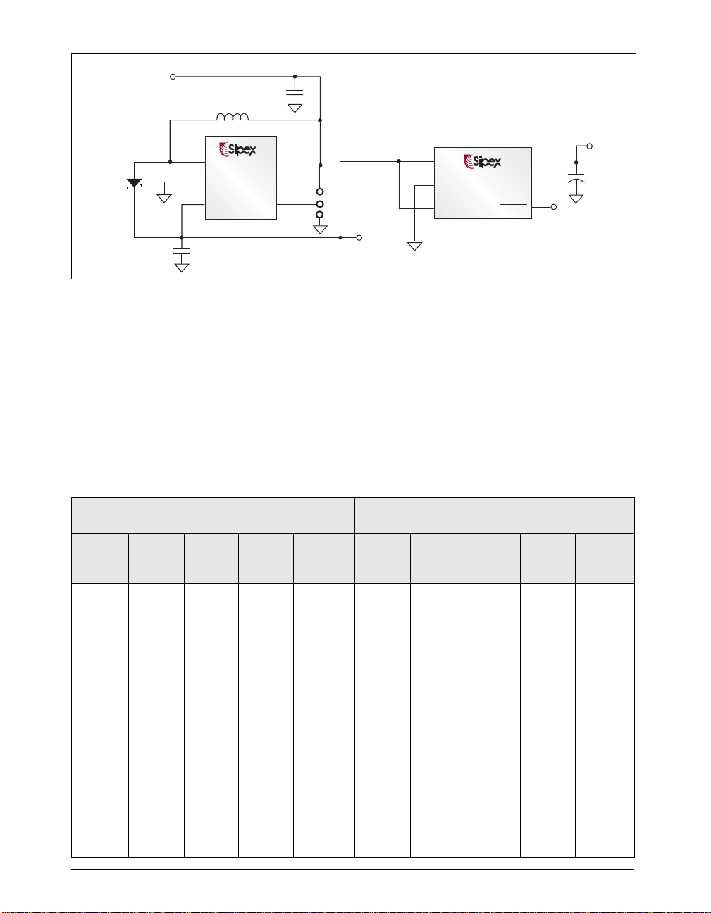
output noise and ripple. The schematic in figure 15
illustrates this circuit on the SP6641A Evaluation
Board with the SP6641 3.3V output followed by
the Sipex SP6201 3.0V output Low Drop Out
linear regulator.
Rev. 5/26/05,
*Patent Pending
SP6641A/6641B 500mA Alkaline DC/DC Boost Regulator in SOT-23 © Copyright 2002 Sipex Corporation
8
Page 9
APPLICATION INFORMATION: continued
Maximum Startup Current
It should be noted that for low input voltages the
SP6641 startup circuit can not support large
load currents at startup. In startup the SP6641
needs to boost the output from zero volts using
a charge pump which has a limited current
capacity. Once the output is greater than 1.7 to
1.9V the operate circuit takes over and the
SP6641 can supply much more current. Curves
of maximum resistive load current in startup for
the SP6641A and SP6641B are shown in Figures 13 & 14 and can be compared with Figure
2, maximum load current in operation. Also,
Table 2 provides SP6641A 3.3V resistive load
current in startup for some low cost 1812 size
From the curves in Figures 13 and 14, you can
see that for low input voltages, the 22µH inductor has more current capacity at startup than the
10µH inductor, due to more energy per charge
cycle in the relationship
1
/2LI2. Thus for 1 cell
applications, 22µH is recommended for more
startup current than 10µH.
For 1-cell battery applications, it is recommended
to apply any large load current after the SP6641
has started up, typically in a few millisecs. This
is typically not a problem in many applications
where the load is a processor whose load current
is low until the processor voltage comes up.
chip inductors.
TABLE 1. COMPONENT SELECTION
INDUCTORS - SURFACE MOUNT
Sipex Inductance Manufacturer/ Series R Isat Size LxWxH Inductor Manufacturer
Part Number (µH) Part Number (Ω) (A) (mm) Type Website
SP6641A Ipk = .33A 22 Sumida CDRH5D28-220 0.095 0.90 5.7x5.5x3 Shielded Ferrite Core www.sumida.com
SP6641A Ipk = .33A 22 Coilcraft DO1608C-223 0.370 0.70 6.6x4.5x2.9 Unshielded Ferrite Core www.coilcraft.com
SP6641A Ipk = .33A 22 TDK NLC453232T-220 0.900 0.37 4.4x3.2x3.2 Unshielded Ferrite Core www.tdk.com
SP6641A Ipk = .33A 22 Murata LQH43C220K04 0.600 0.42 4.5x3.2x2.6 Unshielded Ferrite Core www.murata.com
SP6641B Ipk = 1A 10 Sumida CDRH5D28-100 0.065 1.30 5.7x5.5x3 Shielded Ferrite Core www.sumida.com
SP6641B Ipk = 1A 10 Coilcraft DO1608C-103 0.160 1.10 6.6x4.5x2.9 Unshielded Ferrite Core www.coilcraft.com
SP6641B Ipk = 1A 10 Murata LQH55DN100M01 0.077 1.70 5x5x4.7 Unshielded Ferrite Core www.murata.com
SP6641B Ipk = 1A 22 Sumida CDRH6D28-220 0.128 1.20 6.7x6.5x3 Shielded Ferrite Core www.sumida.com
SP6641B Ipk = 1A 22 Murata LQH55DN220M01 0.160 1.20 5x5x4.7 Unshielded Ferrite Core www.murata.com
Inductor Specification
CAPACITORS - SURFACE MOUNT & THRU-HOLE
Capacitor Specification
Sipex Capacitance Manufacturer/ (max) Current LxWxH Voltage Capacitor Manufacturer
Part Number (µF) Part Number (Ω)@ 45°C (A) (mm) (V) Type Website
SP6641A Ipk = .33A 22 TDK C3225X5R0J226M 0.010 4.00 1210 6.3 SMT X5R Cer. www.tdk.com
SP6641B Ipk = 1A 100 SANYO 10TPA100M 0.080 1.20 7343 6.3 SMT POSCAP Tant. www.sanyovideo.com
SP6641B Ipk = 1A 100 SANYO 16SA100M 0.030 2.70 8Dx10L 16.0 Thru-hole OS-CON www.sanyovideo.com
ESR Ripple Size
SCHOTTKY DIODE - SURFACE MOUNT
Diode Specification
Sipex Manufacturer/ VF @ IF IF(AV) Size LxWxH Reverse V Package Manufacturer
Part Number Part Number (V) (A) (mm) (V) Type Website
SP6641A Ipk = .33A STMicro STPS0520Z 0.39 0.50 3.9x1.7x1.3 20 SOD-123 www.st.com
SP6641B Ipk = 1A Zetex ZCHS2000 0.42 2.00 3x3x1.4 40 SOT23-6 www.zetex.com
Note: Components highlighted in bold are those used on the SP6641A or SP6641B Evaluation Board.
Rev. 5/26/05,
*Patent Pending
SP6641A/6641B 500mA Alkaline DC/DC Boost Regulator in SOT-23 © Copyright 2002 Sipex Corporation
9
Page 10
APPLICATION INFORMATION: continued
+0.9V to +3.3V Input
V
BATT
L1
22µH
1
LX
U1
SP6641
2
D1
C2
22µF
GND
3
V
OUT
+
22µF
®
®
V
BATT
SHDN
+
C1
5
1
4
2
J1
3
V
OUT
+3.3V
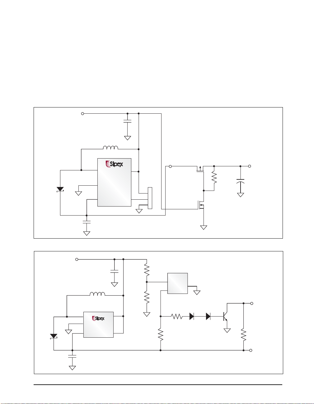
Figure 15. SP6641A 3.3V Evaluation Board with SP6201 LDO Regulator
SuperCap Application on the
SP6641 Output
When the battery input to SP6641A is removed,
the SP6641A output will end up in the charge
mode and will slowly discharge a Supercap
connected to the output. The typical Supercap
of 0.22F will go from fully charged at 3.3V to
less than 2V in 5 minutes. The following appli-
cation circuit in figure 16 is recommended to
disconnect the SP6641 output from the SuperCap
when the battery is removed. The small SOT233pin MOS switches are an inexpensive addition
to the SP6641 circuit and work well to maintain
SuperCap voltage to retain Non-Volatile CMOS
Memory while a battery is changed.
1
V
2
GND
3
ENABLE
V
OUT
+3.0V
®
®
5
V
IN
SP6201
OUT
RESET
C3
1µF
4
TABLE 2. SP6641A Resistive Load Current in Startup - low cost inductors
SP6641A APPLICATION CIRCUIT WITH PANASONIC INDUCTOR SP6641A APPLICATION CIRCUIT WITH TDK INDUCTOR
L1 = ELJ-PB220KF 22µH, IDCmax = 300mA, DCR = 1.0Ω L1 = NLC453232T-220K 22µH, IDCmax = 370mA, DCR = 0.9Ω
Startup V
V
IN
V Ω VmAmA (max) V Ω VmAmA (max)
Load after after then Load after after then
R
(min) Startup Startup Load V
OUT
OUT
I
OUT
Startup Startup V
R
IN
(min) Startup Startup Load
OUT
OUT
I
OUT
0.86 16000 3.31 0.2 37 0.86 16000 3.30 0.2 42
0.88 1500 3.31 2 39 0.88 1500 3.30 2 43
0.90 800 3.30 4 40 0.90 900 3.30 4 44
0.95 230 3.30 14 44 0.95 260 3.30 13 48
1.00 125 3.30 26 48 1.00 126 3.30 26 52
1.10 73 3.29 45 56 1.10 66 3.29 50 60
1.20 58 3.29 57 63 1.20 49 3.29 67 69
1.30 50 3.28 66 71 1.30 43 3.29 77 77
1.40 43 3.28 76 78 1.40 39 3.29 84 84
1.50 39 3.28 84 86 1.50 36 3.29 91 91
Rev. 5/26/05,
*Patent Pending
SP6641A/6641B 500mA Alkaline DC/DC Boost Regulator in SOT-23 © Copyright 2002 Sipex Corporation
10
Startup
Page 11
APPLICATION INFORMATION: continued
Low Battery Circuit for SP6641
Application
The circuit in figure 17 uses the Sipex SPX432
shunt regulator as a reference and comparator
circuit to detect a low battery condition and give
a high level, typically 1.7V output. When the
battery is good, the SPX432 output is low, but
not at ground but at 0.8V or about one Vbe
below the 1.24V reference. To translate that
level to a CMOS Low of less than 0.4V, an NPN
and 2 signal diodes can be added to the SPX432
V
BATT
C1
22µF
L1
22µH
®
®
Diode
Schottky
1
LX
U1
SP6641
2
GND
3
V
OUT
V
BATT
SHDN
5
SHDN
J1
1
2
4
3
output, as shown. The small SOT23-3pin
SPX432 and 2N3904 bipolar transistor and diodes are small and inexpensive to add to the
SP6641 circuit and work well to add a Battery
Low detection circuit, with the addition of about
130µA current from 3.3V out. As a bonus, the
output of this circuit can be used to drive the
SP6641 SHDN_N pin 3 to GND when the battery is removed, which would reset the SP6641
and eliminate the need for the SuperCap Switch
shown in figure 16.
2.7V, 0.9Ω PMOS
SOT23-3 IRLML6302
V
OUT
+3.3V
Q1
32
R1
1M
1
3
Q2 SOT23-3 IRLML2402
1
2.7V NMOS
3.3V to
Nonvolatile Function
C3
.22F Supercap
C2
22µF
Figure 16. SP6641A 3.3V with SuperCap Switch
V
BATT
C1
22µF
L1
22µH
5
V
BATT
®
®
U1
4
SHDN
Diode
Schottky
D1
C2
22µF
1
LX
2
GND
SP6641
3
V
OUT
Figure 17. SP6641A 3.3V with Low Battery Detection
Rev. 5/26/05,
*Patent Pending
SP6641A/6641B 500mA Alkaline DC/DC Boost Regulator in SOT-23 © Copyright 2002 Sipex Corporation
2
1.8V THRES. VTHRES = 1.24V(1 + R1/R2)
R1
44k
R2
100k
R3
20k
1
2
REF
K
100k
U2
SPX432M
SOT23-3
R4
3
A
D2
1N4148
D3
1N4148
Q2
2N3904
11
BATT GOOD
2V = BATT GOOD
0V = LOW BATT
R5
100k
V
3.3V
OUT
Page 12
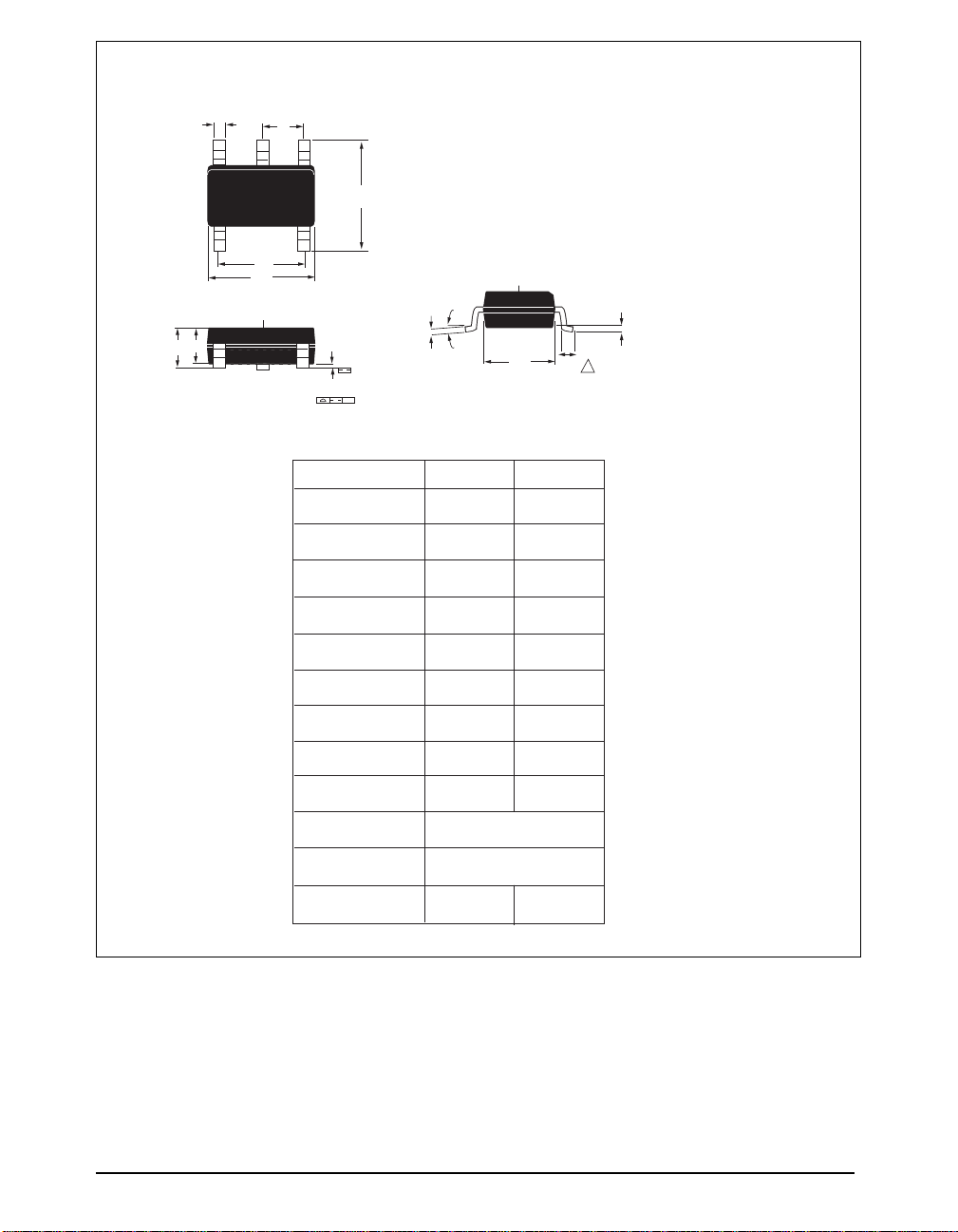
PACKAGE: 5 Lead SOT23
C
L
b
e
E
e1
D
C
L
A2
A
A
A1
A
.10
SYMBOL
A
A1
A2
b
C
D
E
E1
L
a
C
C
L
E1
MIN MAX
0.90
0.00
0.90
0.25
0.09
2.80
2.60
1.50
0.35
1.45
0.15
1.30
0.50
0.20
3.10
3.00
1.75
0.55
DATUM 'A
L
0.20
'
2
Rev. 5/26/05,
*Patent Pending
e
e1
a
SP6641A/6641B 500mA Alkaline DC/DC Boost Regulator in SOT-23 © Copyright 2002 Sipex Corporation
0.95ref
1.90ref
O
0
O
10
12
Page 13
ORDERING INFORMATION
Part Number TOP MARK Temperature Range Package Type
SP6641AEK-3.3/TR ............. K1...................... -40°C to 85°C........
SP6641BEK-3.3/TR ............. L1 ...................... -40°C to 85°C........
SP6641AEK-5.0/TR ............. P1...................... -40°C to 85°C........
SP6641BEK-5.0/TR .............Q1...................... -40°C to 85°C........
(Tape & Reel)
(Tape & Reel)
(Tape & Reel)
(Tape & Reel)
5-Pin SOT-23
5-Pin SOT-23
5-Pin SOT-23
5-Pin SOT-23
Available in lead free packaging. To order add “-L” suffix to part number.
Example: SP6641AEK-3.3/TR = standard; SP6641AEK-L-3.3/TR = lead free, Top Mark “H4”.
/TR = Tape and Reel
Pack quantity is 2,500 for SOT23.
Corporation
SIGNAL PROCESSING EXCELLENCE
Sipex Corporation
Headquarters and
Sales Office
22 Linnell Circle
Billerica, MA 01821
TEL: (978) 667-8700
FAX: (978) 670-9001
e-mail: [email protected]
Sales Office
233 South Hillview Drive
Milpitas, CA 95035
TEL: (408) 934-7500
FAX: (408) 935-7600
Sipex Corporation reserves the right to make changes to any products described herein. Sipex does not assume any liability arising out of the
application or use of any product or circuit described herein; neither does it convey any license under its patent rights nor the rights of others.
Rev. 5/26/05,
*Patent Pending
SP6641A/6641B 500mA Alkaline DC/DC Boost Regulator in SOT-23 © Copyright 2002 Sipex Corporation
13
Page 14

 Loading...