

Page 1
查询SP5658供应商
SP5658
2.7GHz 3-Wire Bus Controlled Frequency Synthesiser
Advance Information
Supersedes October 1996 Media IC Handbook HB3923-2 DS4064 - 4.1 March 1998
The SP5658 is a single chip frequency synthesiser
designed for tuning systems up to 2.7GHz.
The RF preamplifer contains a divide by two prescaler
which can be disabled for applications up to 2GHz so enabling
a step size equal to the comparison frequency up to 2GHz and
twice the comparison frequency up to 2.7GHz.
Comparison frequencies are obtained either from a crystal
controlled on–chip oscillator or from an external source.
The device contains two switching ports, in the 14 pin
version and four in the 16 pin, together with an ‘‘in–lock” flag
output. The device also contains a varactor line disable and
charge pump disable facility.
FEATURES
■ Complete 2.7GHz single chip system
■ Optimised for low phase noise
■ Selectable divide by two prescaler
■ Selectable reference division ratio
■ Charge pump disable
■ Varactor line disable
■ ‘In–lock’ flag
■ Two switching ports in 14 pin version
■ Four switching ports in 16 pin version
■ Pin compatible with SP5659 I 2 C bus low
phase noise synthesiserPP
■ ESD protection (Normal ESD handling procedures
should be observed)
APPLICATIONS
■ SAT, TV, VCR and Cable tuning systems
■ Communications systems
CHARGE PUMP
CRYSTAL
DISABLE
ENABLE
DATA
CLOCK
PORT P1/OC
CHARGE PUMP
CRYSTAL
DISABLE
ENABLE
DATA
CLOCK
PORT P3
PORT P2
114
116116
SP5658S SP5658F
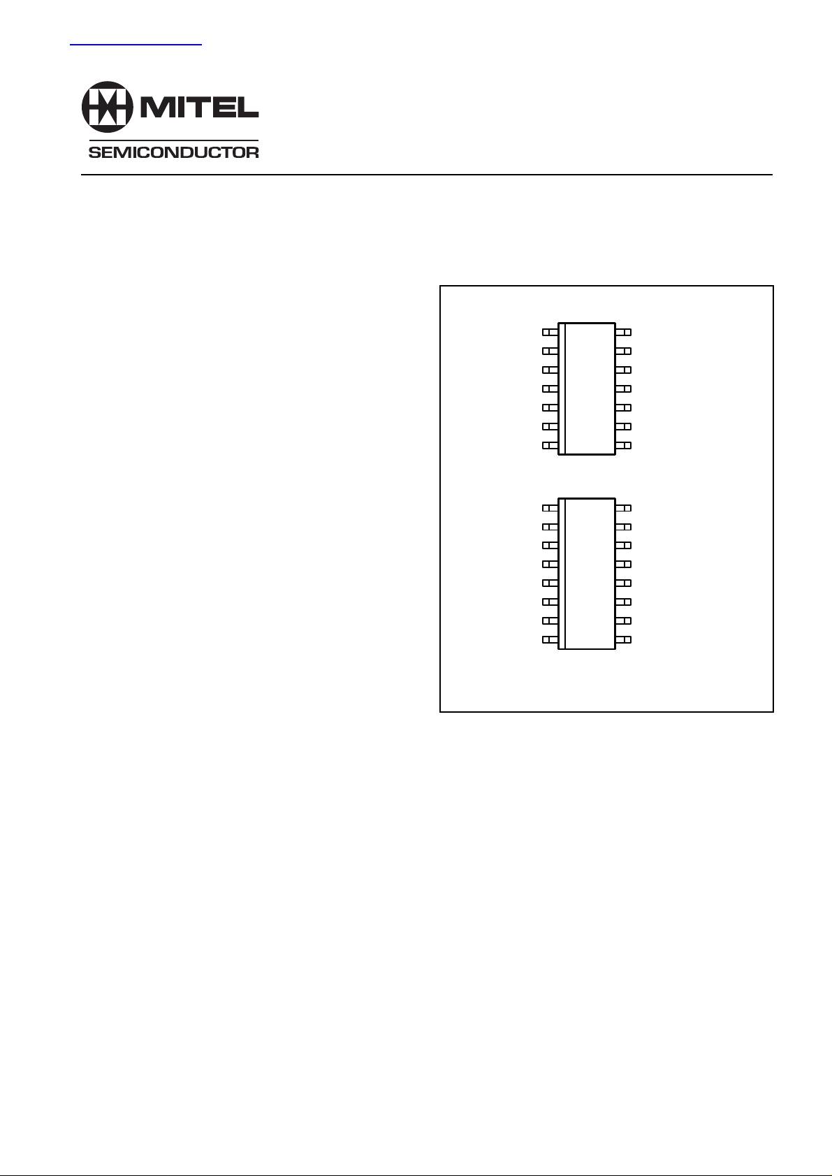
Fig. 1 Pin connections – top view
ORDERING INFORMATION
SP5658F/KG/MP1S (Tubes, 14 lead SO)
SP5658S/KG/MP2S (Tubes, 16 lead SO)
SP5658F/KG/MP1T (Tape and Mounted)
SP5658S/KG/MP2T (Tape and Mounted)
DRIVE
V
EE
RF INPUT
RF INPUT
V
CC
LOCK
PORT P0/OP
DRIVE
V
EE
RF INPUT
RF INPUT
V
CC
LOCK
PORT P0/OP
PORT P1/OC
MP14
MP16
Page 2
SP5658
RF
INPUTS
DISABLE
ENABLE
DATA
CLOCK
13
14
PHASE
PROGRAMMABLE
DIVIDER
-16/17
DE
:
DISABLE
INTERFACE
DATA
4 BIT
COUNT
18 BIT LA
- 2/1
:
3
4
5
6
13 BIT
COUNT
TCH
LA
INTERFACE
P3 P0/OP
COMP
F
pd
CHARGE
PUMP
1 BIT
LATCH
4 BIT
TCH
AND
PORT
89
P2 P1/0C
CO
F
comp
T0
3 BIT LA
(R0,R1,R2)
REFERENCE
DIVIDER
See T
able 1
TCH
1 BIT
LATCH
FLOCK
11107
LOCK
OSC 2
1 BIT
OS
LATCH
CRYSTAL
CHARGE
1
PUMP
16
DRIVE
15
V
12
V
EE
CC
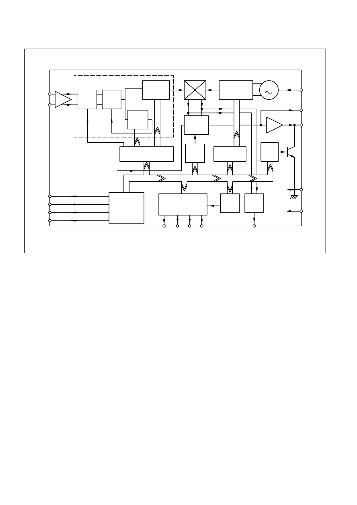
Fig. 2 SP5658S block diagram
2
Page 3
SP5658
ELECTRICAL CHARACTERISTICS
T amb = –20°C to + 80°C, VCC = + 4.5V to + 5.5V. Reference frequency = 4MHz. These characteristics are guaranteed by
either production test or design. They apply within the specified ambient temperature and supply voltage ranges unless otherwise
stated.
Characteristics Pin Units Conditions
Value
(SP5658S)
Supply current, I
CC
12 59 74 mA V
RF input voltage 13, 14 40 300 mV
Min Typ Max
52 65 mA V
=5V Prescaler enabled, DE=1
CC
=5V Prescaler disabled, DE=0
CC
300MHz to 2.7GHz Prescaler
rms
enabled, DE=1, See Fig. 5b
13,14 100 300 mV
80MHz Prescaler enabled,
rms
DE=1, See Fig. 5b.
13, 14 40 300 mV
100MHz to 2.0GHz Prescaler
rms
disabled, DE=0, See Fig. 5a
13,14 50 300 mV
80MHz Prescaler disabled,
rms
DE=0, See Fig. 5a.
RF input impedance 13, 14 50 Ω Refer to Fig. 4
RF input capacitance 13, 14 2 pF Refer to Fig. 4
Data, Clock, Enable & Disable 3,4,5,6
Input high voltage 3 V
CC
V
Input low voltage 0 0.7 V
Input high current 10 µA Input voltage = V
Input low current –10 µA Input voltage = V
Clock Rate 6 500 kHz
Clock data & enable input 4,5,6 0.4 V
hysteresis
CC
EE
3
Page 4
SP5658
ELECTRICAL CHARACTERISTICS
T amb = –20°C to + 80°C, VCC = + 4.5V to + 5.5V. Reference frequency = 4MHz. These characteristics are guaranteed
by either production test or design. They apply within the specified ambient temperature and supply voltage ranges unless
otherwise stated.
Characteristics Pin Value Units Conditions
(SP5658S)
Min Typ Max
Bus Timing 4,5,6
Data set up, t
Data hold, t
Enable set up, t
Enable hold, t
Clock to enable, t
SU
HD
ES
EH
CE
Charge pump output current 1 See Table 3, V
Charge pump output leakage 1 ± 3 ± 10 nA V
Charge pump drive output 16 1 mA V
current
300 ns See Fig. 3
600 ns See Fig. 3
300 ns See Fig. 3
600 ns See Fig. 3
300 ns See Fig. 3
= 2V
PIN1
= 0.7V
PIN16
PIN1
= 2V
Oscillator temperature stability 2 2 ppm/°C
Oscillator supply voltage 2 2 ppm/V
stability
External reference input 2 2 20 MHz AC coupled sinewave
frequency
External reference input 2 200 500 mV
amplitude
AC coupled sinewave
PP
Crystal frequency 2 4 12 MHz
Crystal oscillator drive level 2 45 mV
PP
Recommended crystal series 100 200 Ω Applies to 4MHz crystal only.
resistance ‘‘Parallel resonant” crystal. Figure
quoted is under all conditions
including start up.
Crystal oscillator negative 2 400 Ω Includes temperature and process
resistance tolerances.
Comparison frequency 2 MHz
Phase noise at phase detector –142 dBC/ 6kHz loop BW, phase comparator
Hz freq 250kHz. Figure measured @
1kHz offset, DSB (within loop band
width).
RF division ratio 240 131071 Prescaler disabled, DE=0
480 262142 Prescaler enabled, DE=1
Reference division ratio See Table 1
Output ports P0–P3 # 7,8,9,10
Sink current 10 mA V
Leakage current 10 µAV
PORT
PORT
=0.7V
=13.2V
Lock output 11
Sink current 1 mA V
=0.7V, ‘out of lock’
LOCK
Leakage current 10 µA ‘in lock’
4
# Ports P2 and P3 are not available on the SP5658F.
Page 5
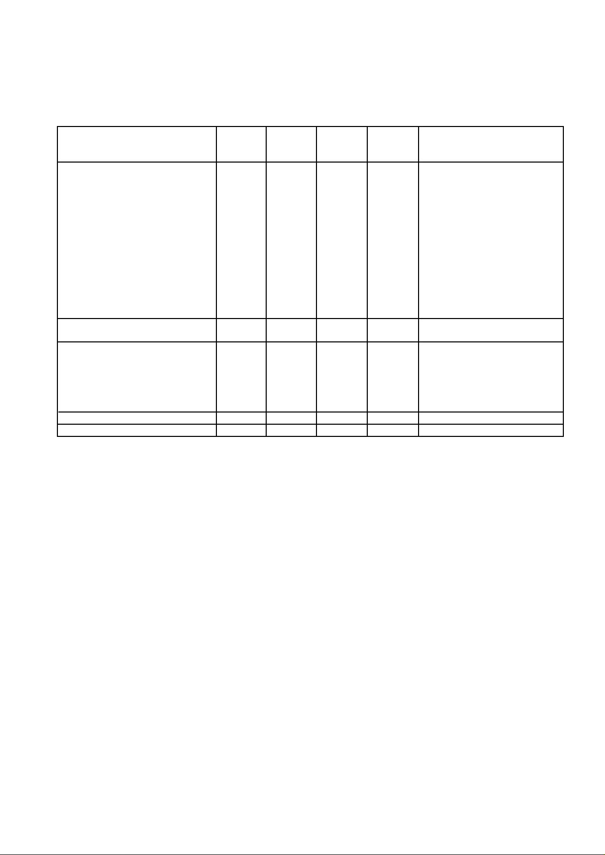
ABSOLUTE MAXIMUM RATINGS
All voltages are referred to V EE at 0V
Characteristics Pin Min Max Units Conditions
(SP5658S)
SP5658
Supply voltage, V
CC
RF input voltage 13, 14 2.5 V
12 –0.3 7 V
p–p
AC coupled as per application
RF input DC offset 13, 14 –0.3 VCC +0.3 V
Port voltage 7 – 10 –0.3 14 V Port in off state
7 – 10 –0.3 6 V Port in on state
Total port current 7 – 10 50 mA
Lock output DC offset 11 –0.3 V
Charge pump DC offset 1 –0.3 V
+0.3 V
CC
+0.3 V
CC
Drive DC offset 16 –0.3 VCC +0.3 V
Crystal DC offset 2 –0.3 VCC +0.3 V
Data, Clock, Enable & Disable DC 3 – 6 –0.3 V
+0.3 V
CC
offset
Storage temperature –55 +125 °C
Junction temperature 150 °C
MP14 Thermal Resistance
Chip to ambient 123 °C/W
Chip to case 45 °C/W
MP16 Thermal Resistance
Chip to ambient 111 °C/W
Chip to case 41 °C/W
Power consumption at V
=5.5V 407 mW All ports off, prescaler enabled
CC
ESD protection ALL 2 kV MIL–STD 883 TM 3015
FUNCTIONAL DESCRIPTION
The SP5658 contains all the elements necessary, with the
exception of a frequency reference, loop filter and external
high voltage transistor, to control a varicap tuned local
oscillator, so forming a complete PLL frequency synthesised
source. The device allows for operation with a high
comparison frequency and is fabricated in high speed logic,
which enables the generation of a loop with good phase noise
performance. The RF preamplifier contains a selectable
divide by two for operation above 2.0GHz. Up to 2GHz the RF
input interfaces directly with the programmable divider, so
eliminating degradation in phase noise due to the prescaler
action. The block diagram is shown in Fig.2.
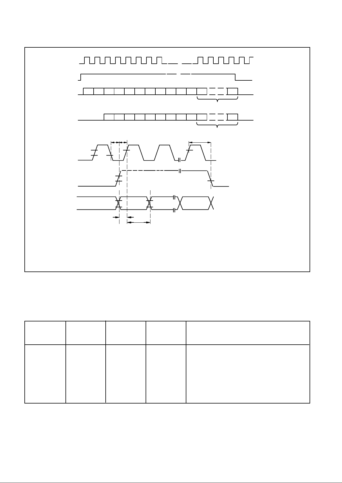
The SP5658 is controlled by a standard 3–wire bus
comprising data, clock and enable inputs. The programming
word for the 16 pin variant contains 28 bits, four of which are
used for port selection, 18 to set the programmable divider
ratio and enable/disable the prescaler, bit DE, three bits to
select the reference division ratio, bits R0–R2, one bit to set
charge pump current, bit C0, and the remaining two bits to
access test modes, bit T0, and to disable the varactor drive,
bit OS. The data word for 14 pin variant is identical to 16 pin
except 26 bits only are required, two of which are used for port
selection. The programming format is shown in Fig. 3.
The clock input is disabled by an enable low signal, data
is therefore only clocked into the internal shift registers during
an enable high and is loaded into the controlling buffers by an
enable high to low transition. This load is also synchronised
with the programmable divider so giving smooth fine tuning.
The RF signal is fed to an internal preamplifier, which
provides gain and reverse isolation from the divider signals.
The output of the preamplifier is fed to the 2/1 selectable
prescaler and then to the 17 bit fully programmable divider,
which is of MN+A architecture. The M counter is 13 bit and the
A counter 4. If bit DE is set to a 0 the prescaler is disabled; Note
that the control function DE cannot be used dynamically.
The output of the programmable divider is fed to the phase
comparator where it is compared in both phase and frequency
domain with the comparison frequency. This frequency is
derived either from the on board crystal controlled oscillator or
from an external source. In both cases the reference
frequency is divided down to the comparison frequency by the
reference divider which is programmable into 1 of 8 ratios as
described in Table 1.
The output of the phase comparator feeds the charge
pump and loop amplifier section, which when used with an
external high voltage transistor and loop filter integrates the
current pulses into the varactor line voltage. The charge pump
can be disabled to a high impedance state by the DISABLE
input. The varactor drive output can also be disabled by the OS
bit within the data word, so switching the external transistor
‘OFF’ and allowing an external voltage to be written to the
varactor line for tuner alignment purposes.
The phase comparator also drives the lock detect circuit
which generates a lock flag. ‘In–lock’ is indicated by a high
impedance state on the lock output.
The programmable divider output divided by 2, F pd /2 and
the comparison frequency, F comp can be switched to ports P0
and P1 respectively by switching the device into test mode.
The test modes are described in Table 2.
5
Page 6
SP5658
CLOCK
ENABLE
16 PIN V
14 PIN V
2
DE
R2 R1 R0,,
P3, P2, P1, P0
CO
OS
T0
DATA
ARIANT
DATA
ARIANT
ENABLE
16
to
CLOCK
DATA
0
2
27226225224223222221220219218217216
2
MSB
P3 P2 P1 P0 TO OS CO R2 R1 R0 DE
25224223222221220219218217216
2
MSB
P1 P0 TO OS CO R2 R1 R0 DE
t
CEtES
3V
0.7V
3V
0.7V
3V
0.7V
t
SU
t
HD
t : Programmable divider ratio control bits
:
- 2 Prescaler (Enable = 1, Disable = 0):
t : Reference divider ratio control bits (see Table1)
t : Port control bits
t : Charge Pump current select (see Table 3)
t : Drive output disable switch
t : T
est mode enable (see Table 2)
0
2
FREQUENCY DATA
0
2
FREQUENCY DATA
t
EH
LSB
MSB IS TRANSMITTED
LSB
t
=Enable set up time
ES
t
=Data set up time
SU
t
=Data hold time
HD
t
=Clock–to–enable time
CE
t
=Enable hold time
EH
FIRST
Fig. 3 Data format and timing
R2 R1 R0 RATIO Comparison Frequency with a 4MHz
external reference.
0 0 0 2 2MHz
0 0 1 4 1MHz
0 1 0 8 500kHz
0 1 1 16 250kHz
1 0 0 32 125kHz
1 0 1 64 62.5kHz
1 1 0 128 31.25kHz
1 1 1 256 15.625kHz
Table 1 Reference division ratios
6
Page 7
SP5658
300
100
40
10
1000 2000
3000
FREQUENCY
(MHz)
3500
OPERATING
WINDOW
1000 2000
2700
3000
FREQUENCY
(MHz)
3500300
OPERATING
WINDOW
300
100
40
10
VIN
(mV RMS
INT
O 50
)
VIN
(mV RMS
INT
O 50
)
100
8080
50
TO OS DIS P0/OP P1/0C FUNCTIONAL DESCRIPTION
0 0 0 # # NORMAL OPERATION
0 0 1 # # CHARGE PUMP DISABLE
1 0 0 F pd/2 F comp NORMAL OPERATION
0 1 0 # # VARACTOR LINE DISABLE
0 1 1 # # CHARGE PUMP AND
VARACTOR LINE DISABLE
1 X 1 – – NOT PERMITTED
# CONTROLLED BY BITS P0 AND P1 WITHIN DATA WORD
Table 2 Test modes
C0 CURRENT IN mA
MIN TYP MAX
0 0.23 0.3 0.37
1 0.68 0.9 1.12
Table 3 Charge pump current
+j1
S11:Z0 = 50
NORMALISED
T
O 50
+j0.2
–j0.2
+j0.5
0.50.2 10
–j0.5
2 5
X
–j1
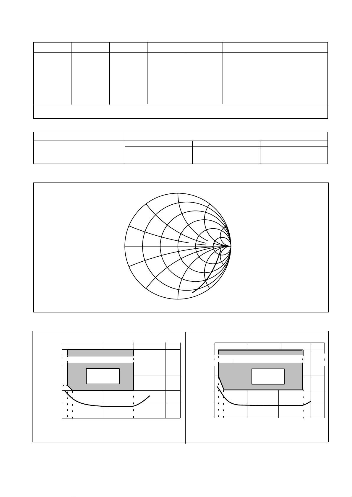
Fig. 4 Typical input impedance
+j2
X
X
–j2
+j5
X
–j5
FREQUENCY
500MHz, 1GHz
MARKERS AT 100MHz,
AND 2.7GHz
Fig. 5a Typical input sensitivity (Prescaler disabled, DE=0) Fig. 5b Typical input sensitivity (Prescaler enabled, DE=1)
7
Page 8
SP5658
DOUBLE CONVERSION TUNER SYSTEMS
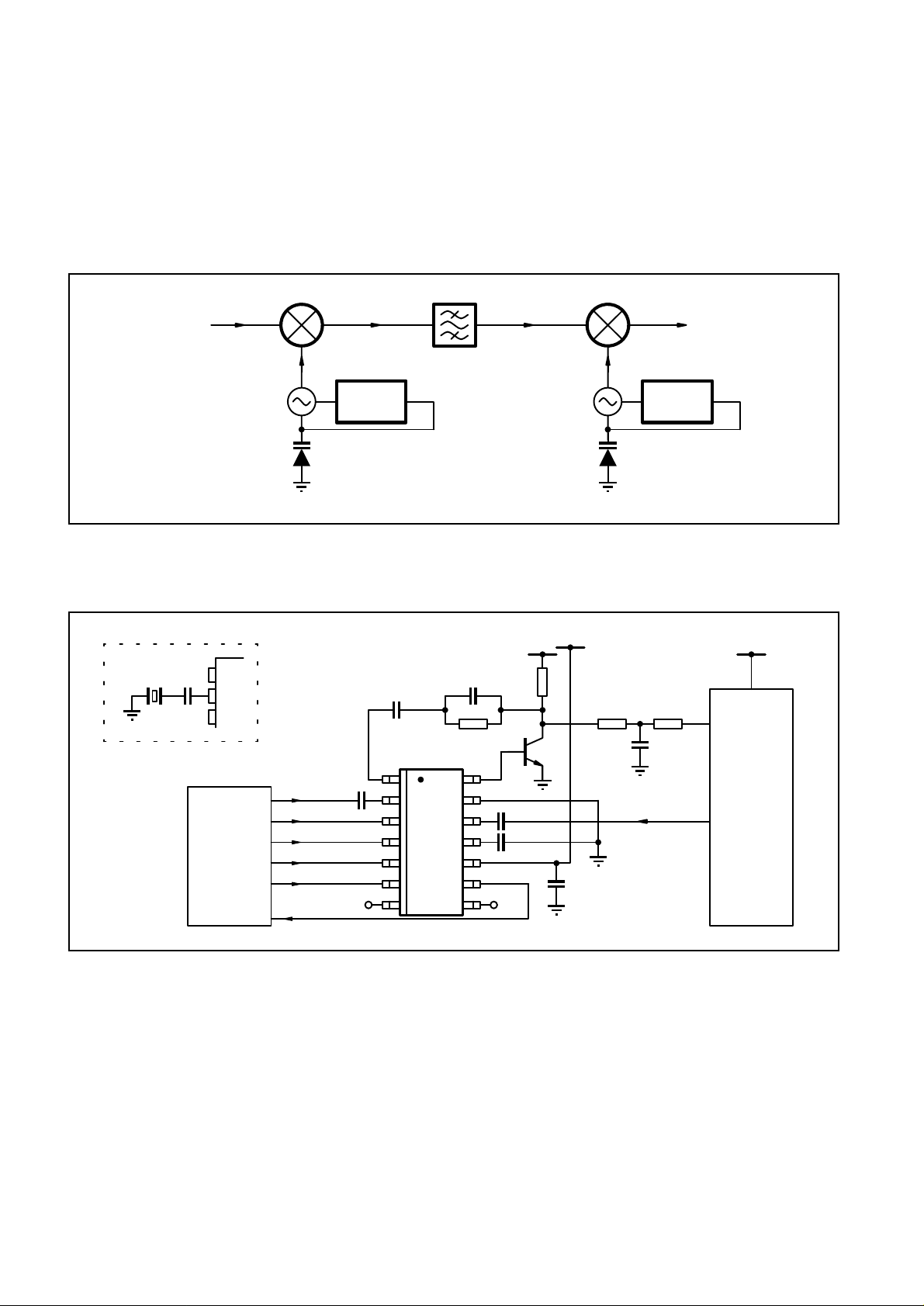
The high 2.7GHz maximum operating frequency and
excellent noise characteristics of the SP5658 enables the
construction of double conversion high IF tuners.
A typical system shown in Fig.7 will use the SP5658 as the
first LO control for full band upconversion to an IF of greater
than 1GHz. The wide range of reference division ratios allows
the SP5658 to be used both for the up converter LO with a high
phase comparator frequency (hence low phase noise) and the
down converter which utilises the device in a lower
comparison frequency mode (which offers a fine step size).
50–900MHz
First LO
Fig. 6 Example of double conversion from VHF/UHF frequencies to TV IF
18pF4MHz
Optional application utilising
on–board crystal controlled
oscillator
CONTROL
MICRO
1.6GHz
1650–2700MHz
SP5658 SP5658
10n
REF
DIS
ENABLE
DATA
CLOCK
P1
LOCK
15nF
114
2
3
4
5
6
7
68pF
13k3
13
12
11
10
SP5658F
9
8
+30V
22k
1n
1n
P0
Second LO
10n
+5V
16k 47k
OSCILLATOR
OUTPUT
38.9MHz
+12V
2n22N3904
TUNER
Fig. 7 Typical application, SP5658F
APPLICATION NOTES
A generic set of application notes AN168 for designing
with synthesisers such as the SP5658 has been written. This
covers aspects such as loop filter design and decoupling. This
application note is also featured in the Media IC Handbook.
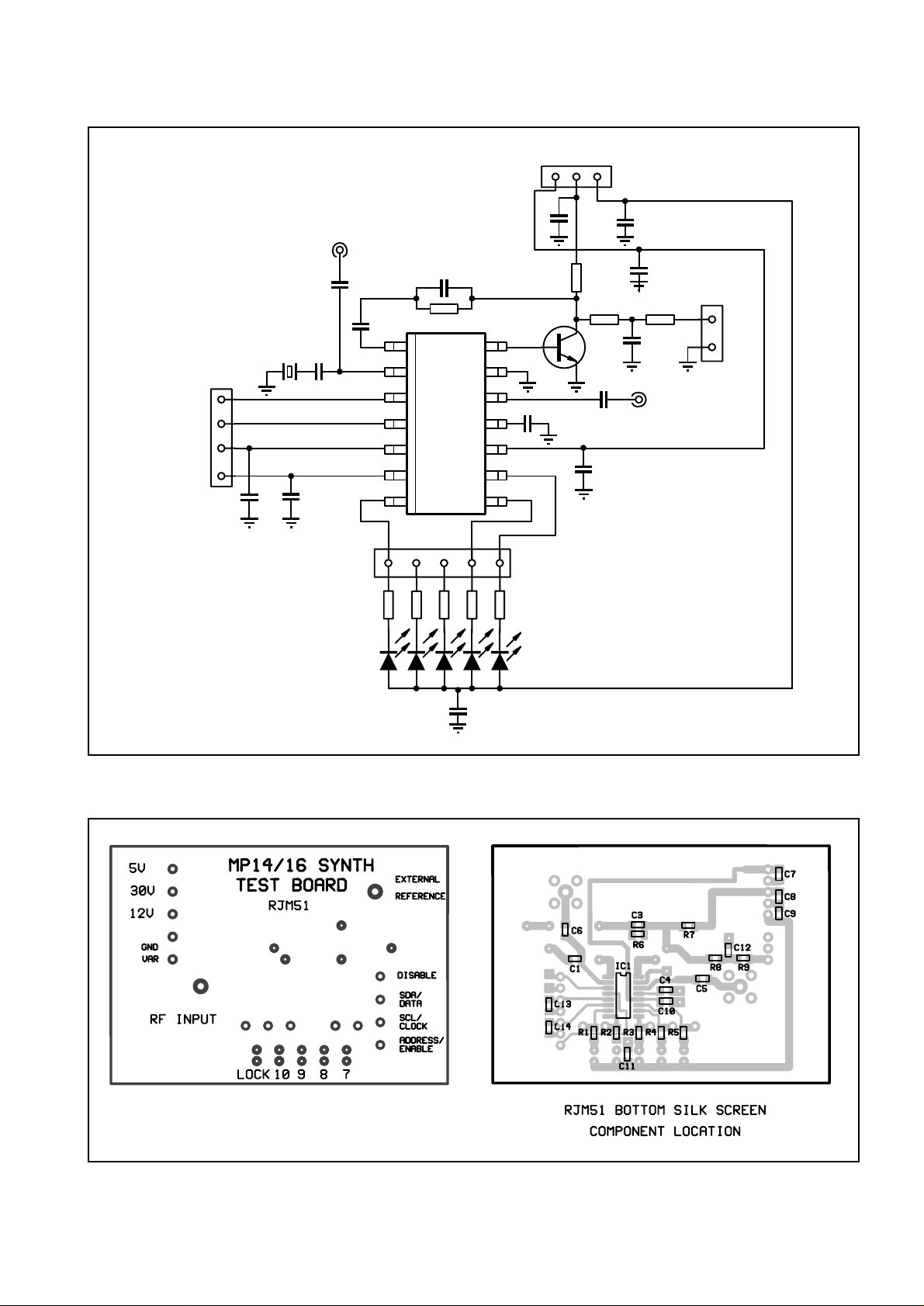
A generic test/demo board has been produced which can
be used for the SP5658. A circuit diagram and layout for the
board is shown in Figs. 8 and 9.
8
The board can be used for the following purposes:
(A) measuring RF sensitivity performance.
(B) Indicating port function.
(C) Synthesising a voltage controlled oscillator.
(D) Testing of external reference sources.
Page 9
+5V
P2
SP5658
+30V
+12V
DISABLE / REF
ENABLE
DATA
/ SDA
CLOCK / SCL
*(NOT FITTED)
X1 4MHz
P1
C13
100pF
EXTERNAL
C6
10nF*
C1
18pF
C14
100pF
REFERENCE
SKT2
C2
15nF
R1 4K7
C3
68pF
R6 13K3
114
13
2
12
3
4
11
5
10
6
7
NC NC
R4 4K7
R3 4K7
R2 4K7
C8
C9
C7/C8/C9 = 100nF
47K
C12
2n2F
SKT1
C7
R9
VAR
GND
RF INPUT
R7
22K
R8
16K
T1
2N3904
C4
1nF
9
8
C5
1nF
C10
1nF
R5 4K7
PIN NO : 7
D5D4D3D2D1
8
LOCK
C11
1nF
Fig. 8 Test board
Fig. 9 Test board (layout)
9
Page 10

SP5658
LOOP BANDWIDTH
The majority of applications for which the SP5658 is
intended require a loop filter bandwidth of between 2kHz and
10kHz.
Typically the VCO phase noise will be specified at both
1kHz and10kHz offset. It is common practice to arrange the
loop filter bandwidth such that the 1kHz figure lies within the
loop bandwidth. Thus the phase noise depends on the
synthesiser comparator noise floor, rather than the VCO.
The 10kHz offset figure should depend on the VCO
providing the loop is designed correctly, and is not
underdamped.
REFERENCE SOURCE
The SP5658 offers optimal LO phase noise performance
when operated with a large step size. This is due to the fact that
the LO phase noise within the loop bandwidth is:
phase comparator
noise floor + 20 log
Assuming the phase comparator noise floor is flat irrespective
of sampling frequency, this means that the best performance
will be achieved when the overall LO to phase comparator
division ratio is a minimum.
There are two ways of achieving a higher phase
comparator sampling frequency:–
A) Reduce the division ratio between the reference source
and the phase comparator
B) use a higher reference source frequency.
Approach B) may be preferred for best performance since it is
possible that the noise floor of the reference oscillator may
degrade the phase comparator performance if the reference
division ratio is very small.
10
( )
LO frequency
phase comparator frequency
10
Page 11
RF INPUTS
V
REF
500 500
SP5658
V
CC
CHARGE
PUMP
25K
RF inputs
V
CC
BIAS
200
OS
(Output disable)
Loop amplifier
PORT/LOCK
DRIVE
OUTPUT
Disable, Enable, Data and Clock inputs
V
CC
CRYSTAL
Reference oscillator
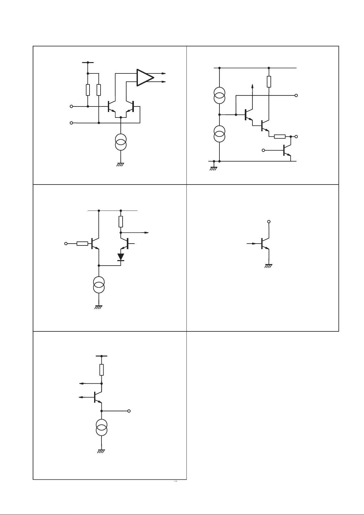
Fig. 10 Input/Output interface circuits
Output Ports and Lock Output
11
Page 12
Page 13
Page 14

M Mitel (design) and ST-BUS are registered trademarks of MITEL Corporation
Mitel Semiconductor is an ISO 9001 Registered Company
Copyright 1999 MITEL Corporation
All Rights Reserved
Printed in CANADA
TECHNICAL DOCUMENTATION - NOT FOR RESALE
World Headquarters - Canada
Tel: +1 (613) 592 2122
Fax: +1 (613) 592 6909
North America Asia/Pacific Europe, Middle East,
Tel: +1 (770) 486 0194 Tel: +65 333 6193 and Africa (EMEA)
Fax: +1 (770) 631 8213 Fax: +65 333 6192 Tel: +44 (0) 1793 518528
Fax: +44 (0) 1793 518581
http://www.mitelsemi.com
Information relating to products and services furnished herein by Mitel Corporation or its subsidiaries (collectively “Mitel”) is believed to be reliable. However, Mitel assumes no
liability for errors that may appear in this publication, or for liability otherwise arising from the application or use of any such information, product or service or for any infringement of
patents or other intellectual property rights owned by third parties which may result from such application or use. Neither the supply of such information or purchase of product or
service conveys any license, either express or implied, under patents or other intellectual property rights owned by Mitel or licensed from third parties by Mitel, whatsoever.
Purchasers of products are also hereby notified that the use of product in certain ways or in combination with Mitel, or non-Mitel furnished goods or services may infringe patents or
other intellectual property rights owned by Mitel.
This publication is issued to provide information only and (unless agreed by Mitel in writing) may not be used, applied or reproduced for any purpose nor form part of any order or
contract nor to be regarded as a representation relating to the products or services concerned. The products, their specifications, services and other information appearing in this
publication are subject to change by Mitel without notice. No warranty or guarantee express or implied is made regarding the capability, performance or suitability of any product or
service. Information concerning possible methods of use is provided as a guide only and does not constitute any guarantee that such methods of use will be satisfactory in a specific
piece of equipment. It is the user’s responsibility to fully determine the performance and suitability of any equipment using such information and to ensure that any publication or
data used is up to date and has not been superseded. Manufacturing does not necessarily include testing of all functions or parameters. These products are not suitable for use in
any medical products whose failure to perform may result in significant injury or death to the user. All products and materials are sold and services provided subject to Mitel’s
conditions of sale which are available on request.
 Loading...