

Page 1
SP5510
1.3GHz Bidirectional I2C BUS Controlled Synthesiser
Supersedes version in April 1994 Consumer IC Handbook, HB3120 - 2.0 DS2184 - 4.0 Janaury 1997
The SP5510 is a single-chip frequency synthesiser designed
for TV tuning systems. Control data is entered in the standard
I2C BUS format. The device has four addressable currentlimited output ports (P0-P3) and four bi-directional opencollector ports (P4-P7), one of which (P6) is also a 3-bit 5-level
ADC input. The information on these ports can be read via the
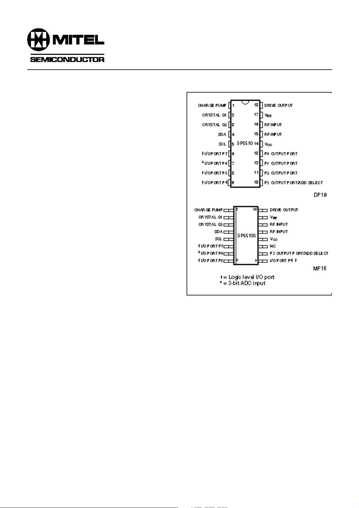
I2C BUS. The SP5510S is a variant in a 16-lead miniature
plastic package, without P0-P2 but functionally identical in
other respects.
Both variants have one fixed I2C BUS address and three
programmable addresses, allowing two or more synthesisers
to be used in a system.
FEATURES
■ Complete 1·3GHz Single Chip System
■ Programmable via the I
■ Low Power Consumption (215mW Typ.)
■ Low Radiation
■ Phase Lock Detector
■ Varactor Drive Amp Disable
■ 8 Controllable Outputs, 4 Bi-directional(SP5510)
■ 5 Controllable Outputs, 4 Bi-directional (SP5510S)
■ 5-Level ADC
■ Variable I
2
C BUS Address for Picture in Picture TV
■ ESD Protection *
* Normal ESD handling precautions should be observed.
2
C BUS
APPLICATIONS
■ Cable Tuning Systems
■ VCRs
ORDERING INFORMATION
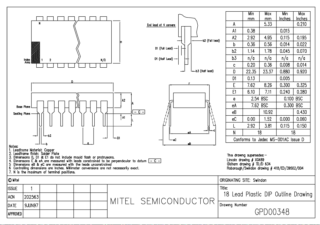
SP5510 NA DP (18-lead plastic package)
SP5510S NA MP (16-lead miniature plastic package)
Fig. 1 Pin connections – top view
Page 2
SP5510
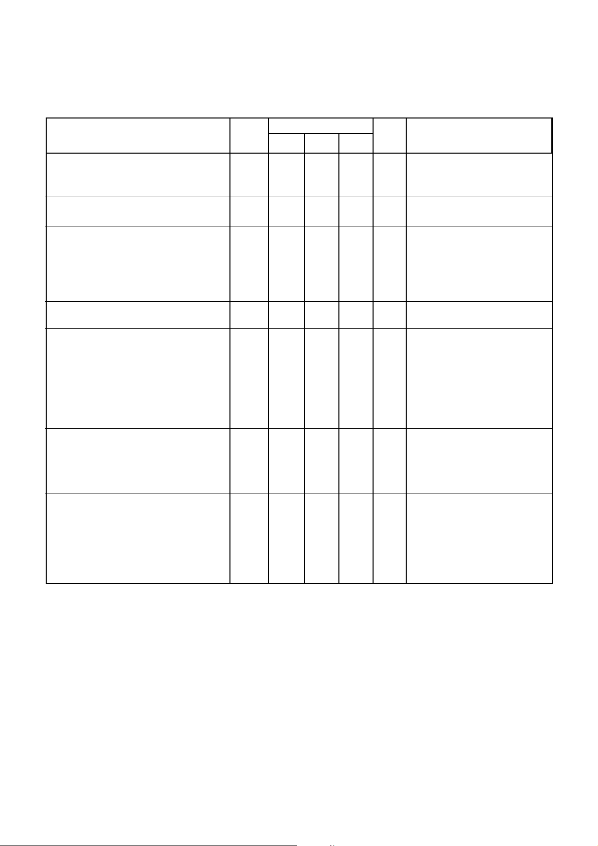
ELECTRICAL CHARACTERISTICS
T
= 210°C to 180°C, VCC = 14·5V to 15·5V. All pin references are to the SP5510 (DP18 package).
AMB
These Characteristics are guaranteed by either production test or design. They apply within the specified ambient temperature
and supply voltage ranges unless otherwise stated. Reference frequency 4MHz unless otherwise stated.
Characteristic Pin
Supply current
Prescaler input voltage
Prescaler input voltage
Prescaler input impedance
Prescaler input capacitance
SDA, SCL
Input high voltage
Input low voltage
Input high current
Input low current
Leakage current
SDA
Output voltage
Charge pump current low
Charge pump current high
Charge pump output leakage current
Charge pump drive output current
Charge pump amplifier gain
Recommended crystal series resistance
Crystal oscillator drive level
Crystal oscillator negative resistance
Output Ports
P0-P3 sink current (see note 1)
P0-P3 leakage current (see note 1)
P4-P7 sink current
P4-P7 leakage current
Input Ports
P3 input current high
P3 input current low
P4, P5, P7 input voltage low
P4, P5, P7 input voltage high
P6 input current high
P6 input current low
14
15,16
15,16
4,5
4,5
4,5
4,5
4,5
4
1
1
1
18
2
10-13
10-13
6-9
6-9
10
10
6,8,9
6,8,9
7
7
Value
Min. Max.
12·5
30
Typ.
43
53
300
300
50
2
3
0
5·5
1·5
10
210
10
0·4
650
6170
65
500
6400
10
200
40
750
0·7
1
1·5
10
10
10
110
210
0·8
2·7
110
210
Units
mA
mVrms
mVrms
Ω
pF
V
V
µA
µA
µA
V
µA
µA
nA
Ω
mV p-p
Ω
mA
µA
mA
µA
µA
µA
V
V
µA
µA
Conditions
VCC = 5V
50MHz to 1GHz
1·3GHz, see Fig. 5
Input voltage = V
CC
Input voltage = 0V
When VCC = 0V
Sink current = 3mA
Byte 4, bit 2 = 0, pin 1 = 2V
Byte 4, bit 2 = 1, pin 1 = 2V
Byte 4, bit 4 = 1, pin 1 = 2V
V pin 18 = 0·7V
Parallel resonant crystal (note 2)
V
= 12V
OUT
V
= 13·2V
OUT
V
= 0·7V
OUT
V
= 13·2V
OUT
V pin 10 = 13·2V
V pin 10 = 0V
See Table 3 for ADC levels
NOTES
1. Ports P0-P2 not present on the SP5510S.
2. The maximum resistance quoted refers to all conditions, including start-up.
2
Page 3
ABSOLUTE MAXIMUM RATINGS
All voltages are referred to VEE and pin 3 at 0V. Pin references are for SP5510 (DP18 package)
SP5510
Parameter
Supply voltage
RF input voltage
Port voltage
Total port output current
RF input DC offset
Charge pump DC offset
Drive output DC offset
Crystal oscillator DC offset
SDA, SCL input voltage
Storage temperature
Junction temperature
DP18 thermal resistance, chip-to-ambient
DP18 thermal resistance, chip-to-case
MP16 thermal resistance, chip-to-ambient
MP16 thermal resistance, chip-to-case
Power consumption at 5·5V
Pin
14
15,16
6-13
6-9
10-13
6-13
15-16
1
18
2
4,5
20·3
20·3
20·3
20·3
20·3
20·3
20·3
20·3
20·3
20·3
255
Value
Max.Min.
7
2·5
14
6
14
50
VCC10·3
VCC10·3
VCC10·3
VCC10·3
VCC10·3
5·5
1150
1150
78
24
111
41
321
Units
V
V p-p
V
V
V
mA
V
V
V
V
V
V
°C
°C
°C/W
°C/W
°C/W
°C/W
mW
Conditions
Port in off state
Port in on state
Port in on state
With VCC applied
V
not applied
CC
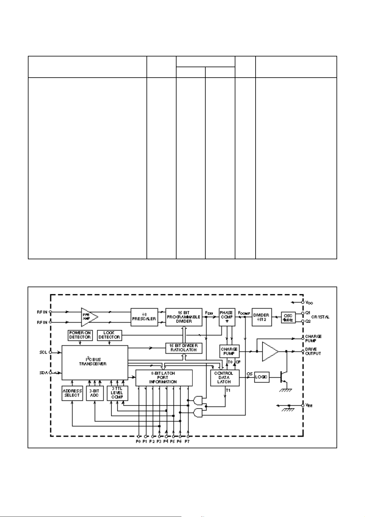
Fig. 2 Block diagram. (Ports P0-P2 not present on SP5510S)
3
Page 4

SP5510
FUNCTIONAL DESCRIPTION
The SP5510 is programmed from an I2C BUS. Data and
Clock are fed in on the SDA and SCL lines respectively as
defined by the I2C Bus format. The synthesiser can either
accept new data (write mode) or send data (read mode). The
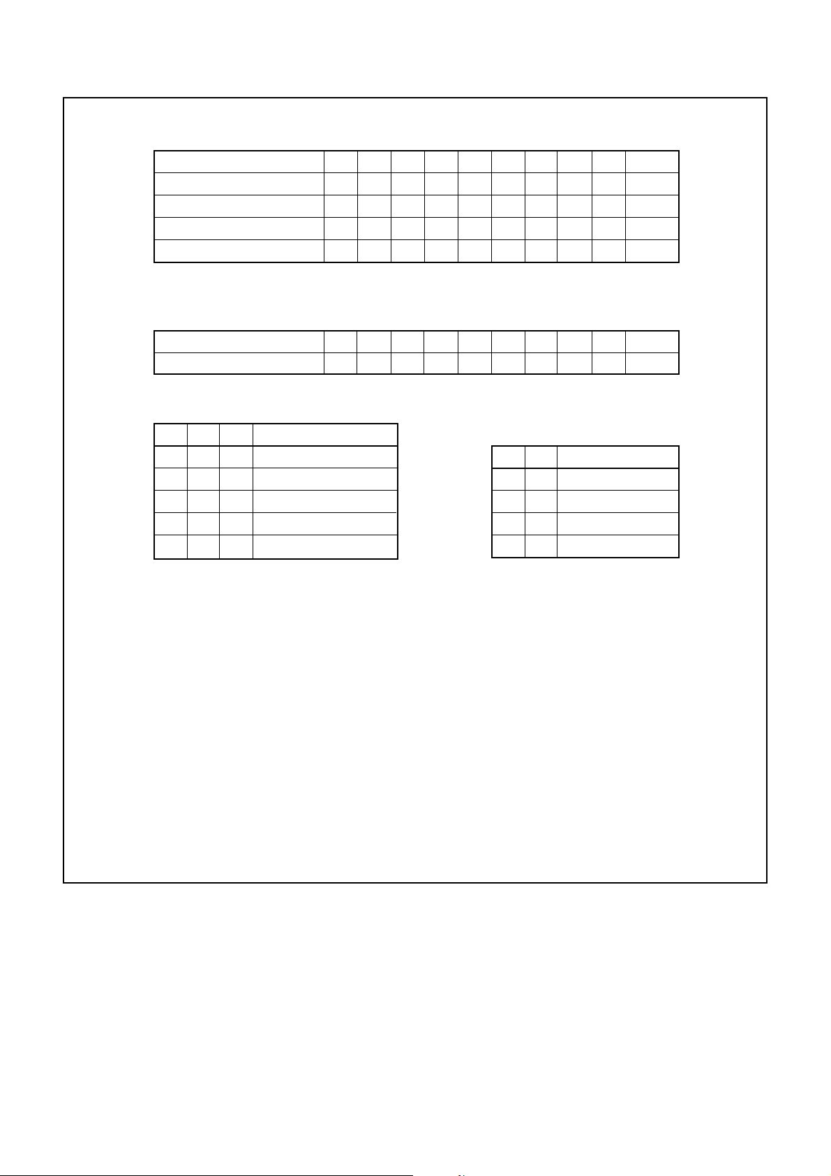
Tables in Fig. 3 illustrate the format of the data. The device
can be programmed to respond to several addresses, which
enables the use of more than one synthesiser in an I2C BUS
system. Table 4 shows how the address is selected by
applying a voltage to P3. The LSB of the address Byte (R/W)
sets the device into read mode if it is high and write mode if
it is low. When the SP5510 receives a correct address Byte
it pulls the SDA line low during the acknowledge period and
during following acknowledge periods after further data Bytes
are programmed. When the SP5510 is programmed into the
read mode the controlling device accepting the data must pull
down the SDA line during the following acknowledge period to
read another status Byte.
WRITE MODE (FREQUENCY SYNTHESIS)
When the device is in the write mode Bytes 213 select the
synthesised frequency while Bytes 415 select the output port
states and charge pump information.
Once the correct address is received and acknowledged,
the first Bit of the next Byte determines whether that Byte is
interpreted as Byte 2 or 4, a logic 0 for frequency information
and a logic 1 for charge pump and output port information.
Additional data Bytes can be entered without the need to readdress the device until an I2C stop condition is recognised.
This allows a smooth frequency sweep for fine tuning or AFC
purposes.
If the transmission of data is stopped mid-byte (i.e., by
another device on the bus) then the previously programmed
byte is maintained.
Frequency data from Bytes 2 and 3 is stored in a 15-bit shift
register and is used to control the division ratio of the 15-bit
programmable divider which is preceded by a divide-by-8
prescaler and amplifier to give excellent sensitivity at the local
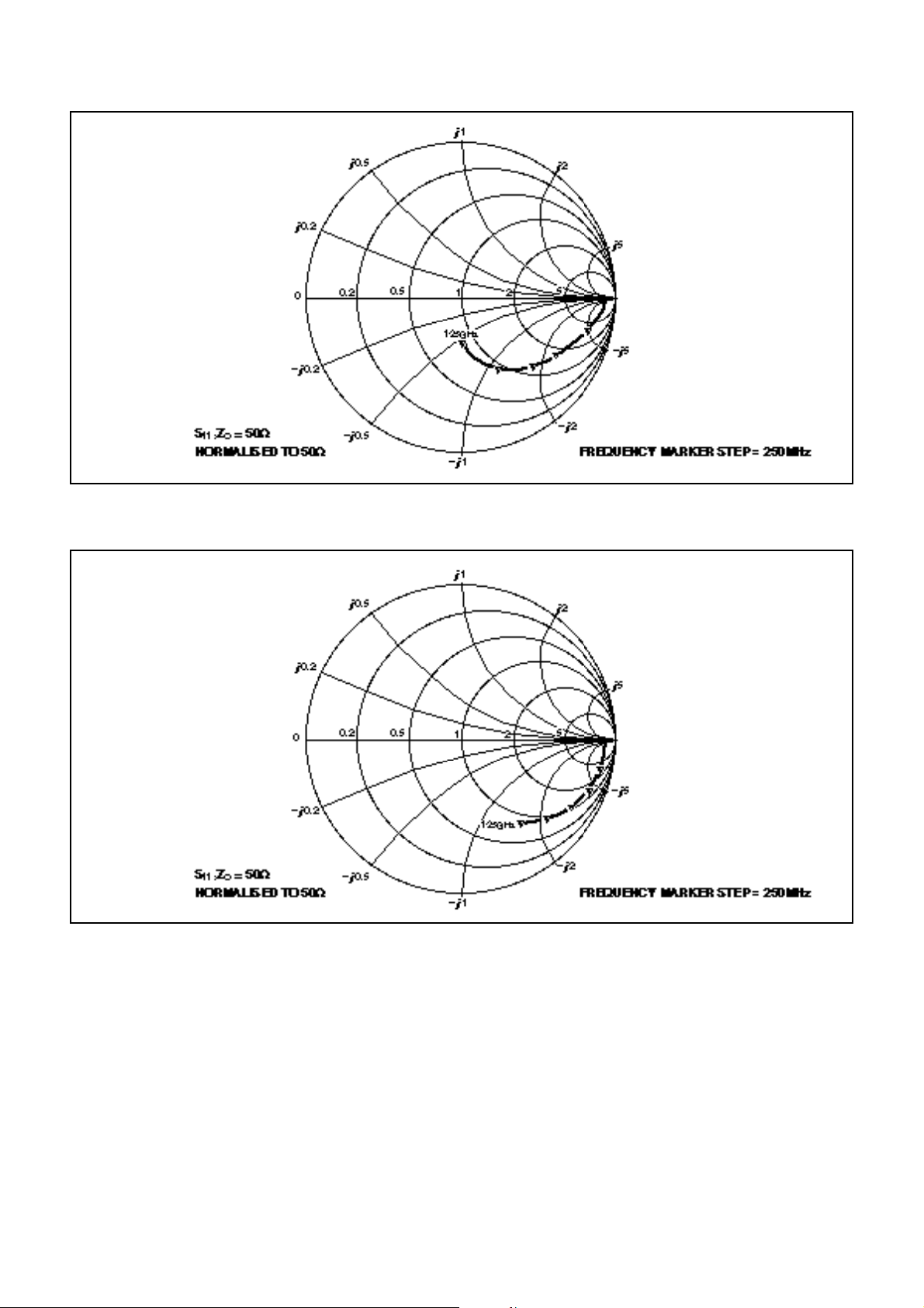
oscillator input; see Fig 5. The input impedance is shown in
Figs. 7 and 8.
The programmed frequency can be calculated by multiplying the programmed division ratio by 8 times the comparison
frequency F
When frequency data is entered, the phase comparator,
via the charge pump and varactor drive amplifier, adjusts the
COMP
.
local oscillator control voltage until the output of the programmable divider is frequency and phase locked to the comparison
frequency.
The reference frequency may be generated by an external
source capacitively coupled into pin 2 or provided by an onchip 4MHz crystal controlled oscillator.
Note that the comparison frequency is 7·8125kHz when a
4MHz reference is used.
Bit 2 of Byte 4 of the programming data (CP) controls the
current in the charge pump circuit, a logic 1 for 6170µA and
a logic 0 for 650µA, allowing compensation for the variable
tuning slope of the tuner and also to enable fast channel
changes over the full band. Bit 4 of Byte 4 (T0) disables the
charge pump if set to a logic 1. Bit 8 of Byte 4 (OS) switches
the charge pump drive amplifier’s output off when it is set to
a logic 1. Bit 3 of Byte 4 (T1) selects a test mode where the
phase comparator inputs are available on P6 and P7, a logic
1 connects F
to P6 and F
COMP
DIV
to P7.
Byte 5 programs the output ports P0-P7, a logic 0 for a high
impedance output, logic 1 for low impedance (on).
READ MODE
When the device is in the read mode the status data read
from the device on the SDA line takes the form shown in Table
2.
Bit 1 (POR) is the power on reset indicator and is set to a
logic 1 if the power supply to the device has dropped below a
nominal 3V and the programmed information lost (e.g., when
the device is initially turned on). The POR is set to 0 when the
read sequence is terminated by a stop command. The outputs
are all set to high impedance when the device is initially
powered up. Bit 2 (FL) indicates whether the device is phase
locked, a logic 1 is present if the device is locked and a logic
0 if the device is unlocked.
Bits 3, 4 and 5 (I2, I1, I0) show the status of the I/O Ports
P7, P5 and P4 respectively. A logic 0 indicates a low level and
a logic 1 a high level. If the ports are to be used as inputs they
should be programmed to a high impedance state (logic1).
These inputs will then respond to data complying with standard TTL voltage levels. Bits 6, 7 and 8 (A2,A1,A0) combine to
give the output of the 5-level ADC.
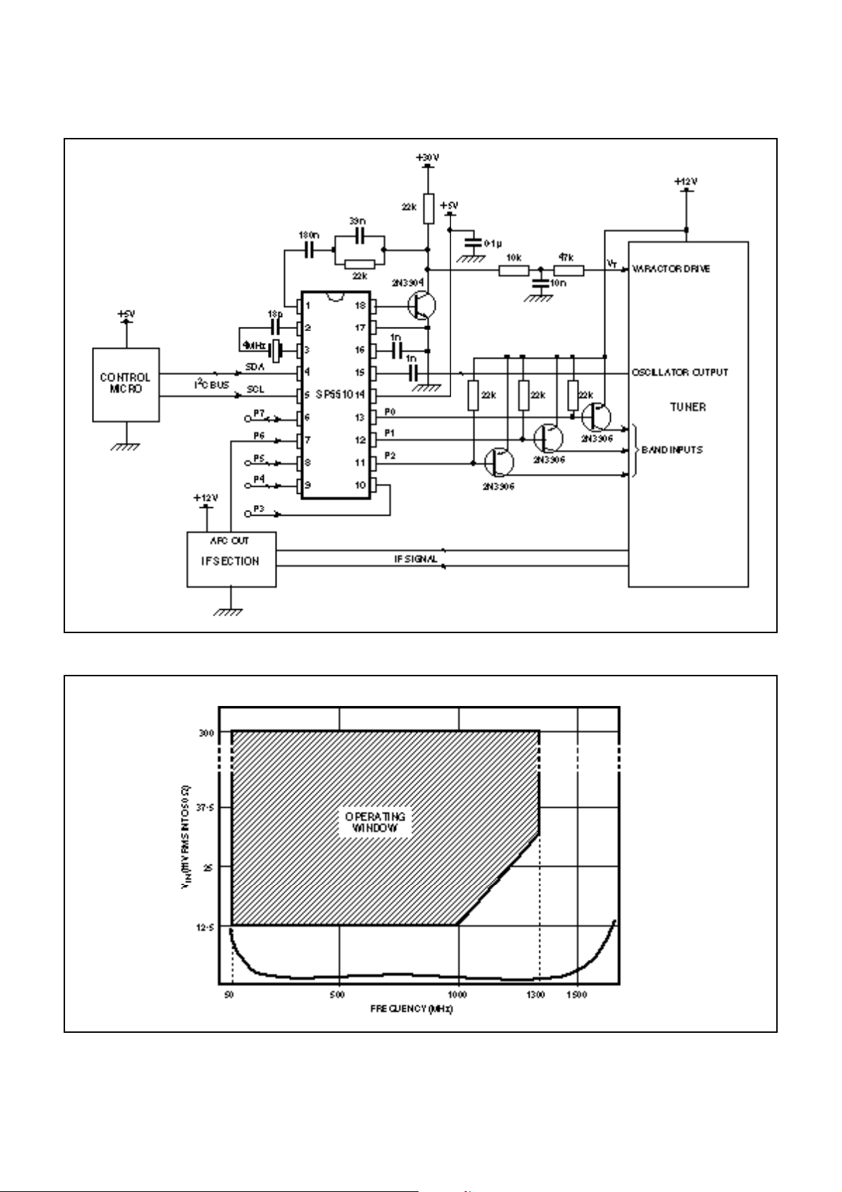
The 5-level ADC can be used to feed AFC information to
the microprocessor from the IF section of the television, as
illustrated in Fig. 4.
4
Page 5
SP5510
Address
Programmable divider
Programmable divider
Charge pump and test bits
I/O port control bits
Table 1 Write data format (MSB transmitted first)
Address
Status byte
A2
A1
0
1
1
0
1
0
0
0
0
0
Voltage input to P6
A0
0
1
0
1
0
0·6V
0·45V
0·3V
0·15V
0V to 0·15V
CC
CC
CC
CC
Table 3 ADC levels
MSB
1
1
0
2
1
P7
1
7
0
14
13
2
2
6
5
2
2
CP
T1
P6
P5
1FL0I20I10
POR
Table 2 Read data format
to 13·2V
to 0·6V
CC
to 0·45V
to 0·3V
CC
CC
CC
2
2
T0
P4
LSB
0
0
12
11
2
4
3
2
1
P3
I0
MA1
10
2
2
2
1
P2*
MA1
A2
MA1
0
0
1
1
MA0
MA0
MA0
0
9
8
2
2
1
0
2
2
1
OS
P1*
P0*
1
A1
A0
Voltage input to P3
0
1
0
1
0V to 0·2V
Always valid
0·3VCC to 0·7V
0·8VCC to 13·2V
Byte 1
A
Byte 2
A
Byte 3
A
Byte 4
A
Byte 5
A
Byte 1
A
Byte 2
A
CC
CC
Table 4 Address selection
A : Acknowledge bit
MA1, MA0 : Variable address bits (see Table 4)
CP : Charge Pump current select
T1 : Test mode selection
T0 : Charge pump disable
OS : Varactor drive Output disable Switch
P7, P6, P5, P4, : Control output port states
P3, P2*, P1*, P0*
POR : Power On Reset indicator
FL : Phase lock detect flag
I2, I1, I0 : Digital information from ports P7, P5 and P4 respectively
A2, A1, A0 : 5-level ADC data from P6 (see Table 3)
NOTE
Don’t care condition on SP5510S.
*
Fig. 3 Data formats
5
Page 6
SP5510
APPLICATION
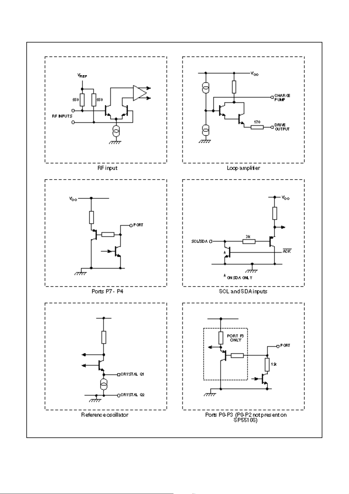
A typical application is shown in Fig. 4. All input/output interface circuits are shown in Fig. 6.
Fig. 4 Typical application
Fig. 5 Typical input sensitivity
6
Page 7
SP5510
Fig. 6 SP5510 input/output interface circuits
7
Page 8
SP5510
Fig. 7 Typical input impedance, SP5510
Fig. 8 Typical input impedance, SP5510S
8
Page 9
Page 10

http://www.mitelsemi.com
World Headquarters - Canada
Tel: +1 (613) 592 2122
Fax: +1 (613) 592 6909
North America Asia/Pacific Europe, Middle East,
Tel: +1 (770) 486 0194 Tel: +65 333 6193 and Africa (EMEA)
Fax: +1 (770) 631 8213 Fax: +65 333 6192 Tel: +44 (0) 1793 518528
Fax: +44 (0) 1793 518581
Information relating to products and services furnished herein by Mitel Corporation or its subsidiaries (collectively “Mitel”) is believed to be reliable. However, Mitel assumes no
liability for errors that may appear in this publication, or for liability otherwise arising from the application or use of any such information, product or service or for any infringement of
patents or other intellectual property rights owned by third parties which may result from such application or use. Neither the supply of such information or purchase of product or
service conveys any license, either express or implied, under patents or other intellectual property rights owned by Mitel or licensed from third parties by Mitel, whatsoever.
Purchasers of products are also hereby notified that the use of product in certain ways or in combination with Mitel, or non-Mitel furnished goods or services may infringe patents or
other intellectual property rights owned by Mitel.
This publication is issued to provide information only and (unless agreed by Mitel in writing) may not be used, applied or reproduced for any purpose nor form part of any order or
contract nor to be regarded as a representation relating to the products or services concerned. The products, their specifications, services and other information appearing in this
publication are subject to change by Mitel without notice. No warranty or guarantee express or implied is made regarding the capability, performance or suitability of any product or
service. Information concerning possible methods of use is provided as a guide only and does not constitute any guarantee that such methods of use will be satisfactory in a specific
piece of equipment. It is the user’s responsibility to fully determine the performance and suitability of any equipment using such information and to ensure that any publication or
data used is up to date and has not been superseded. Manufacturing does not necessarily include testing of all functions or parameters. These products are not suitable for use in
any medical products whose failure to perform may result in significant injury or death to the user. All products and materials are sold and services provided subject to Mitel’s
conditions of sale which are available on request.
M Mitel (design) and ST-BUS are registered trademarks of MITEL Corporation
Mitel Semiconductor is an ISO 9001 Registered Company
Copyright 1999 MITEL Corporation
All Rights Reserved
Printed in CANADA
TECHNICAL DOCUMENTATION - NOT FOR RESALE
 Loading...