

Page 1

®
PRELIMINARY
SP3508
Rugged 3.3V, 20Mbps, 8 Channel Multiprotocol Transceiver
with Programmable DCE/DTE and Termination Resistors
FEATURES
■ Fast 20Mbps Differential Transmission Rates
■ Internal Transceiver Termination Resistors
for V.11 & V.35
■ Interface Modes:
✓ RS-232 (V.28) ✓ EIA-530 (V.10 & V.11)
✓ X.21 (V.11) ✓ EIA-530A (V.10 & V.11)
✓ RS-449/V.36 ✓ V.35 (V.35 & V.28)
(V.10 & V.11)
■ Protocols are Software Selectable with 3-Bit Word
■ Eight (8) Drivers and Eight (8) Receivers
■ Termination Network Disable Option
■ Internal Line or Digital Loopback for Diagnostic Testing
■ Certified conformance to NET1/NET2 and TBR-1
TBR-2 by TUV Rheinland (TBR2/30451940.001/04)
■ Easy Flow-Through Pinout
■ +3.3V Only Operation
■ Individual Driver and Receiver Enable/Disable Controls
■ Operates in either DTE or DCE Mode
The SP3508 is a monolithic device that supports eight (8) popular serial interface standards
for Wide Area Network (WAN) connectivity. The SP3508 is fabricated using a low power
BiCMOS process technology, and incorporates a Sipex regulated charge pump allowing
+3.3V only operation. Sipex's patented charge pump provides a regulated output of +5.5V,
which will provide enough voltage for compliant operation in all modes. Eight (8) drivers and
eight (8) receivers can be configured via software for any of the above interface modes at any
time. The SP3508 requires no additional external components for compliant operation for all
of the eight (8) modes of operation other than six capacitors used for the internal charge pump.
All necessary termination is integrated within the SP3508 and is switchable when V.35 drivers
and V.35 receivers, or when V.11 receivers are used. The SP3508 provides the controls and
transceiver availability for operating as either a DTE or DCE.
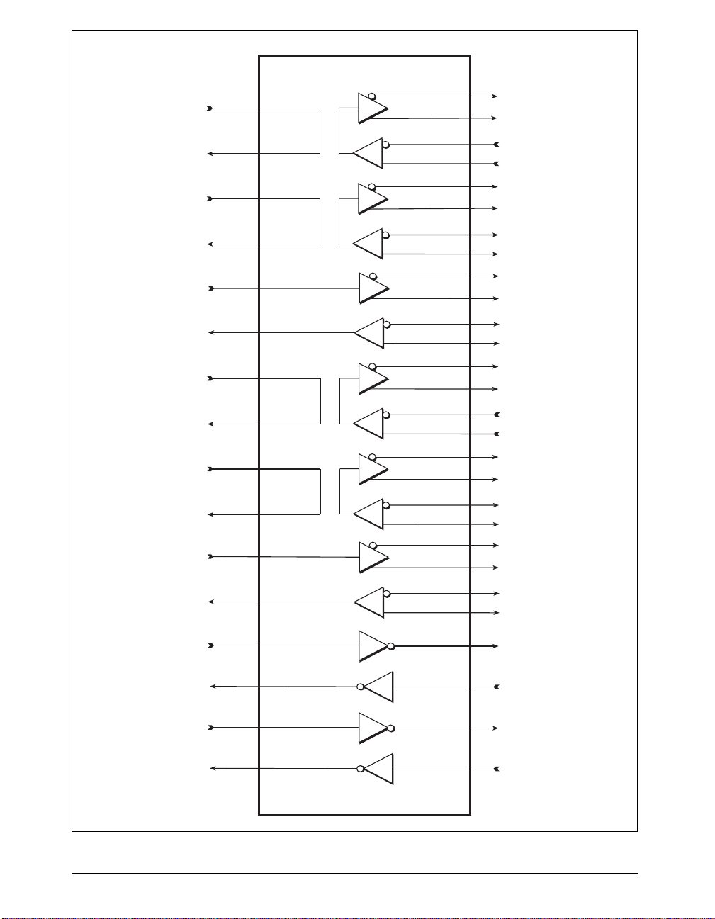
Additional features with the SP3508 include internal loopback that can be initiated in any of the
operating modes by use of the LOOPBACK pin. While in loopback mode, receiver outputs are
internally connected to driver inputs creating an internal signal path bypassing the serial
communications controller for diagnostic testing. The SP3508 also includes a latch enable pin
with the driver and receiver address decoder. The internal V.11 or V.35 termination can be
switched off using a control pin (TERM_OFF) for monitoring applications. All eight (8) drivers and
receivers in the SP3508 include separate enable pins for added convenience. The SP3508 is
ideal for WAN serial ports in networking equipment such as routers, access concentrators,
network muxes, DSU/CSU's, networking test equipment, and other access devices.
Now Available in Lead Free Packaging
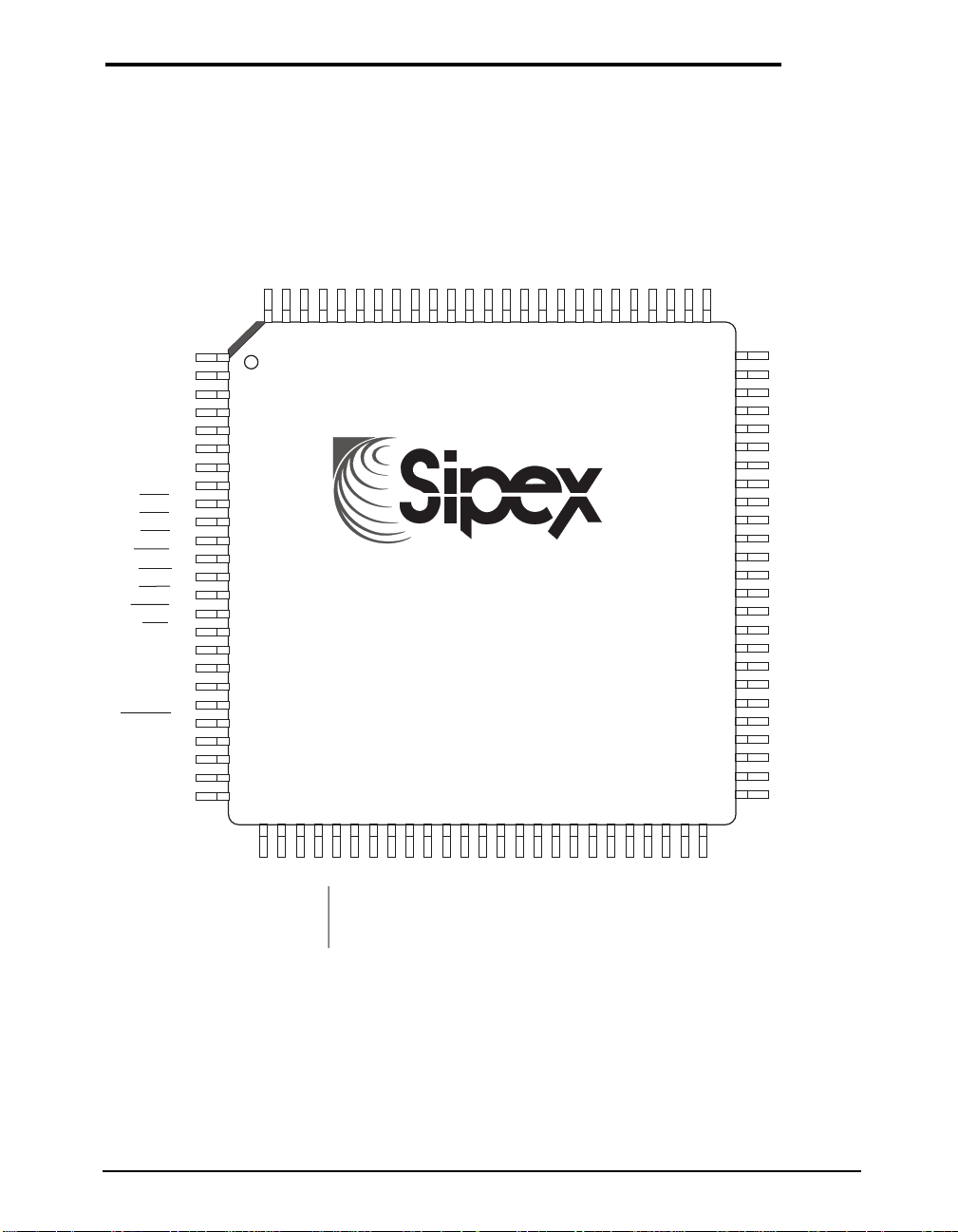
Refer to page 9 for pinout
APPLICATIONS
■ Router
■ Frame Relay
■ CSU
■ DSU
■ PBX
■ Secure Communication Terminals
DESCRIPTION
Applicable U.S. Patents-5,306,954; and others patents pending
Date: 10/12/04 SP3508 Enhanced WAN Multi–Mode Serial Transceiver © Copyright 2004 Sipex Corporation
1
Page 2
ABSOLUTE MAXIMUM RATINGS
VCC................................................................................................ +7V
Input Voltages:
Output Voltages:
Storage Temperature ................................................ -65
Power Dissipation ................................................................. 1520mW
(derate 19.0mW/°C above +70°C)
Logic ................................................ -0.3V to (VCC+0.5V)
Drivers ............................................. -0.3V to (V
Receivers ........................................................... ±15.5V
Logic ................................................ -0.3V to (V
Drivers ................................................................... ±12V
Receivers ........................................ -0.3V to (V
+0.5V)
CC
+0.5V)
CC
+0.5V)
CC
°C to +150°C
Package Derating:
ø
.................................................................................................................
JA
....................................................................................................................
ø
JC
These are stress ratings only and functional operation of the
device at these ratings or any other above those indicated in the
operation sections of the specifications below is not implied.
Exposure to absolute maximum rating conditions for extended
periods of time may affect reliability.
STORAGE CONSIDERATIONS
Due to the relatively large package size of the 100-pin quad flatpack, storage in a low humidity environment is preferred. Large
high density plastic packages are moisture sensitive and should
be stored in Dry Vapor Barrier Bags. Prior to usage, the parts
should remain bagged and stored below 40°C and 60%RH. If
the parts are removed from the bag, they should be used within
48 hours or stored in an environment at or below 20%RH. If the
above conditions cannot be followed, the parts should be
baked for four hours at 125°C in order to remove moisture prior
to soldering. Sipex ships the 100-pin LQFP in Dry Vapor
Barrier Bags with a humidity indicator card and desiccant pack.
The humidity indicator should be below 30%RH.
ELECTRICAL SPECIFICATIONS
TA = 0 to 70°C and VCC = 3.3V ± 5% unless otherwise noted. The ♦ denotes the specifications which apply over the full operating
temperature range (-40
V
LI
V
HI
V
LO
V
HO
°C to +85°C), unless otherwise specified.
RETEMARAP.NIM.PYT.XAMSTINUSNOITIDNOC
STUPNICIGOL
♦♦♦♦♦
8.0
0.2
V
♦♦♦♦♦
V
STUPTUOCIGOL
♦♦♦♦♦
VCC-
4.0
VCC-
6.0
3.0
VAm2.3–=TUOI
♦♦♦♦♦
V
Am0.1=TUOI
36.9 °C/W
6.5 °C/W
)stuptuO(sretemaraPCDREVIRD82.V
stuptuO
egatloVtiucriCnepO51±
egatloVdedaoL0.5±51±
tnerruCtiucriC-trohS001±
ecnadepmIffO-rewoP003
)stuptuO(sretemaraPCAREVIRD82.V V
emiTnoitisnarT5.1
♦♦♦♦♦
V1erugiFrep
♦♦♦♦♦
V2erugiFrep
♦♦♦♦♦
Am4erugiFrep
♦♦♦♦♦Ω
♦♦♦♦♦
sµV3-otV3+,6erugiFrep
5erugiFrep
CC
sretemarapCArofV3.3+=
etaRwelSsuoenatnatsnI03sµ/V3erugiFrep
t:yaleDnoitagaporP
LHP
t:yaleDnoitagaporP
HLP
5.00.10.3
5.00.10.3
etaRnoissimsnarT.xaM021032
Date: 10/12/04 SP3508 Enhanced WAN Multi–Mode Serial Transceiver © Copyright 2004 Sipex Corporation
♦♦♦♦♦
sµ
♦♦♦♦♦
sµ
♦♦♦♦♦
spbk
2
Page 3
ELECTRICAL SPECIFICATIONS
TA = 0 to 70°C and VCC = 3.3V ± 5% unless otherwise noted. The ♦ denotes the specifications which apply over the full operating
temperature range (-40
ytivitisneS3.0±
°C to +85°C), unless otherwise specified.
RETEMARAP.NIM.PYT.XAMSTINUSNOITIDNOC
)stupnI(sretemaraPCDREVIECER82.V
ecnadepmItupnI37
saiBtiucriC-nepO0.2+
dlohserhTHGIH7.10.3
dlohserhTWOL8.02.1
sretemaraPCAREVIECER82.V V
t:yaleDnoitagaporP
LHP
t:yaleDnoitagaporP
HLP
001005sn
001005sn
♦♦♦♦♦
kΩ 7erugiFrep
♦♦♦♦♦
V8erugiFrep
♦♦♦♦♦
V
♦♦♦♦♦
V
CC
etaRnoissimsnarTxaM021532spbk
)stuptuO(sretemaraPCDREVIRD01.V
egatloVtiucriCnepO0.4±0.6±
egatloVdetanimreT-tseTV9.0
CO
♦♦♦♦♦
V9erugiFrep
V01erugiFrep
tnerruCtiucriC-trohS051±Am11erugiFrep
tnerruCffO-rewoP001±
)stuptuO(sretemaraPCAREVIRD01.V V
emiTnoitisnarT002
t:yaleDnoitagaporP
LHP
t:yaleDnoitagaporP
HLP
001005
001005
etaRnoissimsnarTxaM021
♦♦♦♦♦
Aµ21erugiFrep
CC
♦♦♦♦♦
sn%09ot%01;31erugiFrep
♦♦♦♦♦
sn
♦♦♦♦♦
sn
♦♦♦♦♦
spbk
)stupnI(sretemaraPCDREVIECER01.V
tnerruCtupnI52.3-52.3+Am51dna41serugiFrep
ecnadepmItupnI4
sretemaraPCAREVIECER01.V V
t:yaleDnoitagaporP
LHP
t:yaleDnoitagaporP
HLP
021052
021052
etaRnoissimsnarTxaM021
♦♦♦♦♦
kΩ
♦♦♦♦♦
V
CC
♦♦♦♦♦
sn
♦♦♦♦♦
sn
♦♦♦♦♦
spbk
sretemarapCArofV3.3+=
sretemarapCArofV3.3+=
sretemarapCArofV3.3+=
Date: 10/12/04 SP3508 Enhanced WAN Multi–Mode Serial Transceiver © Copyright 2004 Sipex Corporation
3
Page 4
ELECTRICAL SPECIFICATIONS
TA = 0 to 70°C and VCC = 3.3V ± 5% unless otherwise noted. The ♦ denotes the specifications which apply over the full operating
temperature range (-40
ecnalaB4.0±V 71erugiFrep
tesffO0.3+
ytivitisneS2.0±
wekS501sn23erugiFrep
°C to +85°C), unless otherwise specified.
RETEMARAP.NIM.PYT.XAMSTINUSNOITIDNOC
)stuptuO(sretemaraPCDREVIRD11.V
)0.6±
V(egatloVtiucriCnepO
CO
egatloVdetanimreTtseT0.2±
)
5.0V(
CO
♦♦♦♦♦
♦♦♦♦♦
♦♦♦♦♦
♦♦♦♦♦
tnerruCtiucriC-trohS051±
tnerruCffO-rewoP001±
♦♦♦♦♦
♦♦♦♦♦
)stuptuO(sretemaraPCAREVIRD11.V V
emiTnoitisnarT01
t:yaleDnoitagaporP
LHP
t:yaleDnoitagaporP
HLP
0306
0306
wekSlaitnereffiD501
etaRnoissimsnarT.xaM02
♦♦♦♦♦
♦♦♦♦♦
♦♦♦♦♦
♦♦♦♦♦
♦♦♦♦♦
)stupnI(sretemaraPCDREVIECER11.V
egnaRedoMnommoC7-7+
♦♦♦♦♦
♦♦♦♦♦
tnerruCtupnI52.3-52.3±
Ω001/wtnerruC
noitanimreT
ecnadepmItupnI4
-7.06±
5
♦♦♦♦♦
sretemaraPCAREVIECER11.V V
t:yaleDnoitagaporP
LHP
t:yaleDnoitagaporP
HLP
0306sn73dna23serugiFrep
0306sn73dna23serugiFrep
etaRnoissimsnarTxaM02spbM
V61erugiFrep
V71erugiFrep
V
V71erugiFrep
Am81erugiFrep
Aµ91erugiFrep
sn
sn53dna23serugiFrep
sn53dna23serugiFrep
sn53dna23serugiFrep
spbM
V
V
Am
Am
kΩ
CC
;Fp05=LCgnisU%09
ffo
42dna32erugiFrep
CC
Fp05=LCgnisU
sretemarapCArofV3.3+=
ot%01;53dna12serugiFrep
ronorewop;22dna02erugiFrep
sretemarapCArofV3.3+=
Date: 10/12/04 SP3508 Enhanced WAN Multi–Mode Serial Transceiver © Copyright 2004 Sipex Corporation
4
Page 5
ELECTRICAL SPECIFICATIONS
TA = 0 to 70°C and VCC = 3.3V ± 5% unless otherwise noted. The ♦ denotes the specifications which apply over the full operating
temperature range (-40
tesffO6.0±
ytivitisneS05±002±
wekS501snC;23serugiFrep
tnerruC
°C to +85°C), unless otherwise specified.
RETEMARAP.NIM.PYT.XAMSTINUSNOITIDNOC
)stuptuO(sretemaraPCDREVIRD53.V
egatloVtiucriCnepO02.1±V 61erugiFrep
egatloVdetanimreTtseT44.0±66.0±V 52erugiFrep
♦♦♦♦♦
V52erugiFrep
toohsrevOtuptuO-V2.0-
TS
ecnadepmIecruoS05051
ecnadepmItiucriC-trohS531561
)stuptuO(sretemaraPCAREVIRD53.V V
emiTnoitisnarT02
t:yaleDnoitagaporP
LHP
t:yaleDnoitagaporP
HLP
0306
0306
wekSlaitnereffiD5
etaRnoissimsnarT.xaM02
-2.0+
V
TS
♦♦♦♦♦
V
♦♦♦♦♦Ω
Ω
♦♦♦♦♦
sn
♦♦♦♦♦
snC;53dna23serugiFrep
♦♦♦♦♦
snC;53dna23serugiFrep
♦♦♦♦♦
snC;53dna23serugiFrep
♦♦♦♦♦
spbM
eulav
CC
72erugiFrep
V;52erugiFrep
TS
Z;62erugiFrep
SV=2V/1
L
L
L
)stupnI(sretemaraPCDREVIECER53.V
♦♦♦♦♦
Vm
ecnadepmIecruoS09011
ecnadepmItiucriC-trohS531561
sretemaraPCAREVIECER53.V V
t:yaleDnoitagaporP
LHP
t:yaleDnoitagaporP
HLP
0306snC;73dna23serugiFrep
0306snC;73dna23serugiFrep
Ω
Ω
CC
03erugiFrep
Z;92erugiFrep
SV=2V/1
L
L
L
Fp02=
etaRnoissimsnarT.xaM02spbM
STNERRUCEGAKAELREVIECSNART
tnerruCetatS-3tuptuOrevirD002AµdelbasidsrevirD;13erugiFrep
etatS-3tuptuOrevieceR
101
D
111=
X
Aµ
05x
05x Ω
sretemarapCArofV5+=
etatsydaetS=
sretemarapCArofV3.3+=
Fp02=
Fp02=
Fp02=
Fp02=
Fp02=
Date: 10/12/04 SP3508 Enhanced WAN Multi–Mode Serial Transceiver © Copyright 2004 Sipex Corporation
5
Page 6
ELECTRICAL SPECIFICATIONS
TA = 0 to 70°C and VCC = 3.3V ± 5% unless otherwise noted. The ♦ denotes the specifications which apply over the full operating
temperature range (-40
°C to +85°C), unless otherwise specified.
RETEMARAP.NIM.PYT.XAMSTINUSNOITIDNOC
STNEMERIUQERREWOP
V
CC
I
CC
)detceleSedoMoN(1
)232-SR/82.V59
)224-SR/11.V(032
)944-SR&035-AIE(072
)53.V(071
51.33.354.3V
♦♦♦♦♦
♦♦♦♦♦
♦♦♦♦♦
♦♦♦♦♦
♦♦♦♦♦
AµIllA
f
NI
Am
Amf
NI
Amf
NI
Am
CC
dedaol
Vhtiweraseulav
V3.3+=
CC
&evitcasrevirD;spbk032=
dedaol&evitcasrevirD;spbM02=
dedaol&evitcasrevirD;spbM02=
If@53.V
N
spbk032
@82.V,spbM02=
Date: 10/12/04 SP3508 Enhanced WAN Multi–Mode Serial Transceiver © Copyright 2004 Sipex Corporation
6
Page 7
OTHER AC CHARACTERISTICS
TA = 0 to 70°C and VCC = +3.3V unless otherwise noted.
PARAMETER MIN. TYP. MAX. UNITS CONDITIONS
DRIVER DELAY TIME BETWEEN ACTIVE MODE AND TRI-STATE MODE
RS-232/V.28
t
; Tri-state to Output LOW 0.70 5.0 µsC
PZL
; Tri-state to Output HIGH 0.40 2.0 µsC
t
PZH
t
; Output LOW to Tri-state 0.20 2.0 µsC
PLZ
t
; Output HIGH to Tri-state 0.40 2.0 µsC
PHZ
RS-423/V.10
t
; Tri-state to Output LOW 0.15 2.0 µsC
PZL
t
; Tri-state to Output HIGH 0.20 2.0 µsC
PZH
t
; Output LOW to Tri-state 0.20 2.0 µsC
PLZ
t
; Output HIGH to Tri-state 0.15 2.0 µsC
PHZ
RS-422/V.11
t
; Tri-state to Output LOW 2.80 10.0 µsC
PZL
t
; Tri-state to Output HIGH 0.10 2.0 µsC
PZH
t
; Output LOW to Tri-state 0.10 2.0 µsC
PLZ
t
; Output HIGH to Tri-state 0.10 2.0 µsC
PHZ
V.35
t
; Tri-state to Output LOW 2.60 10.0 µsC
PZL
t
; Tri-state to Output HIGH 0.10 2.0 µsC
PZH
t
; Output LOW to Tri-state 0.10 2.0 µsC
PLZ
t
; Output HIGH to Tri-state 0.15 2.0 µsC
PHZ
RECEIVER DELAY TIME BETWEEN ACTIVE MODE AND TRI-STATE MODE
RS-232/V.28
t
; Tri-state to Output LOW 0.12 2.0 µsC
PZL
t
; Tri-state to Output HIGH 0.10 2.0 µsC
PZH
t
; Output LOW to Tri-state 0.10 2.0 µsC
PLZ
t
; Output HIGH to Tri-state 0.10 2.0 µsC
PHZ
RS-423/V.10
t
; Tri-state to Output LOW 0.10 2.0 µsC
PZL
t
; Tri-state to Output HIGH 0.10 2.0 µsC
PZH
t
; Output LOW to Tri-state 0.10 2.0 µsC
PLZ
t
; Output HIGH to Tri-state 0.10 2.0 µsC
PHZ
= 100pF, Fig. 33 & 39; S
L
= 100pF, Fig. 33 & 39; S
L
= 100pF, Fig. 33 & 39; S
L
= 100pF, Fig. 33 & 39; S
L
= 100pF, Fig. 33 & 39; S
L
= 100pF, Fig. 33 & 39; S
L
= 100pF, Fig. 33 & 39; S
L
= 100pF, Fig. 33 & 39; S
L
= 100pF, Fig. 33 & 36; S
L
= 100pF, Fig. 33 & 36; S
L
= 15pF, Fig. 33 & 36; S
L
= 15pF, Fig. 33 & 36; S
L
= 100pF, Fig. 33 & 36; S
L
= 100pF, Fig. 33 & 36; S
L
= 15pF, Fig. 33 & 36; S
L
= 15pF, Fig. 33 & 36; S
L
= 100pF, Fig. 34 & 37; S
L
= 100pF, Fig. 34 & 37; S
L
= 100pF, Fig. 34 & 37; S
L
= 100pF, Fig. 34 & 37; S
L
= 100pF, Fig. 34 & 37; S
L
= 100pF, Fig. 34 & 37; S
L
= 100pF, Fig. 34 & 37; S
L
= 100pF, Fig. 34 & 37; S
L
closed
1
closed
2
closed
1
closed
2
closed
1
closed
2
closed
1
closed
2
closed
1
closed
2
closed
1
closed
2
closed
1
closed
2
closed
1
closed
2
closed
1
closed
2
closed
1
closed
2
closed
1
closed
2
closed
1
closed
2
Date: 10/12/04 SP3508 Enhanced WAN Multi–Mode Serial Transceiver © Copyright 2004 Sipex Corporation
7
Page 8

OTHER AC CHARACTERISTICS: Continued
TA = 0 to 70°C and VCC = +3.3V unless otherwise noted.
PARAMETER MIN. TYP. MAX. UNITS CONDITIONS
RS-422/V.11
t
; Tri-state to Output LOW 0.10 2.0 µsC
PZL
t
; Tri-state to Output HIGH 0.10 2.0 µsC
PZH
t
; Output LOW to Tri-state 0.10 2.0 µsC
PLZ
t
; Output HIGH to Tri-state 0.10 2.0 µsC
PHZ
V.35
t
; Tri-state to Output LOW 0.10 2.0 µsC
PZL
t
; Tri-state to Output HIGH 0.10 2.0 µsC
PZH
t
; Output LOW to Tri-state 0.10 2.0 µsC
PLZ
t
; Output HIGH to Tri-state 0.10 2.0 µsC
PHZ
TRANSCEIVER TO TRANSCEIVER SKEW (per Figures 32, 35, 37)
RS-232 Driver 100 ns [ (t
100 ns [ (t
RS-232 Receiver 20 ns [ (t
20 ns [ (t
RS-422 Driver 2 ns [ (t
2ns[ (t
RS-422 Receiver 3 ns [ (t
3ns[ (t
RS-423 Driver 5 ns [ (t
5ns[ (t
RS-423 Receiver 5 ns [ (t
5ns[ (t
V.35 Driver 4 ns [ (t
4ns[ (t
V.35 Receiver 6 ns [ (t
6ns[ (t
= 100pF, Fig. 34 & 38; S
L
closed
= 100pF, Fig. 34 & 38; S
L
closed
= 15pF, Fig. 34 & 38; S
L
closed
= 15pF, Fig. 34 & 38; S
L
closed
= 100pF, Fig. 34 & 38; S
L
closed
= 100pF, Fig. 34 & 38; S
L
closed
= 15pF, Fig. 34 & 38; S
L
closed
= 15pF, Fig. 34 & 38; S
L
closed
)
– (t
phl
Tx1
)
– (t
plh
Tx1
)
– (t
phl
Rx1
)
– (t
phl
Rx1
)
– (t
phl
Tx1
)
– (t
plh
Tx1
)
– (t
phl
Rx1
)
– (t
phl
Rx1
)
– (t
phl
Tx2
)
– (t
plh
Tx2
)
– (t
phl
Rx2
)
– (t
phl
Rx2
)
– (t
phl
Tx1
)
– (t
plh
Tx1
)
– (t
phl
Rx1
)
– (t
phl
Rx1
phl
plh
phl
phl
phl
plh
phl
phl
phl
plh
phl
phl
phl
plh
phl
phl
)
)
)
)
)
)
)
)
)
)
)
)
)
)
)
)
Txn
Txn
Rxn
Rxn
Txn
Txn
Rxn
Rxn
Txn
Txn
Rxn
Rxn
Txn
Txn
Rxn
Rxn
1
2
1
2
1
2
1
2
]
]
]
]
]
]
]
]
]
]
]
]
]
]
]
]
Date: 10/12/04 SP3508 Enhanced WAN Multi–Mode Serial Transceiver © Copyright 2004 Sipex Corporation
8
Page 9
100 VCC
99 SD(b)
98 VCC
97 SD(a)
96 GND
95 TT(b)
94 VCC
93 TT(a)
92 GND
91 ST(b)
90 VCC
89 ST(a)
88 GND
87 TR(b)
86 VCC
85 TR(a)
84 GND
83 RS(b)
82 VCC
81 RS(a)
80 GND
79 RRC(a)
78 VCC
77 RCC(b)
PINOUT
76 VDD
GND 1
SDEN
TTEN
STEN 4
RSEN
TREN 6
RRCEN 7
RLEN 8
LLEN 9
RDEN 10
RTEN 11
TXCEN 12
CSEN13
DMEN 14
RRTEN 15
ICEN 16
TMEN 17
D0 18
D1 19
D2 20
D_LATCH 21
TERM_OFF 22
VCC 23
C3P 24
GND 25
2
3
5
®
SP3508
C3N 26
VSS2 27
AVCC 29
AGND 28
LOOPBACK 30
31
TXD
ST 33
TXCE 32
RTS 34
35
DTR
LL 38
RL 37
RXD 39
DCD_DCE 36
TXC 41
RXC 40
CTS 42
DSR 43
RI 45
TM 46
GND 47
DCD_DTE 44
VCC 48
RD(b) 49
RD(a) 50
75 GND
74 C1P
73 VCC
72 C2P
71 GND
70 C1N
69 C2N
68 VSS1
67 RL(a)
66 VCC
65 LL(a)
64 TM(a)
63 IC
62 RRT(a)
61 RRT(b)
60 GNDV10
59 DM(a)
58 DM(b)
57 CS(a)
56 CS(b)
55 TXC(a)
54 GND
53 TXC(b)
52 RT(a)
51 RT(b)
Date: 10/12/04 SP3508 Enhanced WAN Multi–Mode Serial Transceiver © Copyright 2004 Sipex Corporation
9
Page 10
SP3508 Pin Designation
Pin Number Pin Name Description Pin Number Pin Name Description
1 GND Signal Ground 51 RT(B) RxC Non-Inverting Input
2 SDEN TxD Driver Enable Input 52 RT(A) RxC Inverting Input
3 TTEN TxCE Driver Enable Input 53 TxC(B) TxC Non-Inverting Input
4 STEN ST Driver Enable Input 54 GND Signal Ground
5 RSEN RTS Driver Enable Input 55 TxC(A) TxC Inverting Input
6 TREN DTR Driver Enable Input 56 CS(B) CTS Non-Inverting Input
7 RRCEN DCD Driver Enable Input 57 CS(A) CTS Inverting Input
8 RLEN RL Driver Enable Input 58 DM(B) DSR Non-Inverting Input
9 LLEN LL Driver Enable Input 59 DM(A) DSR Inverting Input
10 RDEN RxD Receiver Enable Input 60 GNDV10 V.10 Rx Reference Node
11 RTEN RxC Receiver Enable Input 61 RRT(B) DCD
12 TxCEN TxC Receiver Enable Input 62 RRT(A) DCD
Non-Inverting Input
DTE
Inverting Input
DTE
13 CSEN CTS Receiver Enable Input 63 IC RI Receiver Input
14 DMEN DSR Receiver Enable Input 64 TM(A) TM Receiver Input
15 RRTEN DCD
Receiver Enable Input 65 LL(A) LL Driver Output
DTE
16 ICEN RI Receiver Enable Input 66 VCC Power Supply Input
17 TMEN TM Receiver Enable Input 67 RL(A) RL Driver Output
18 D0 Mode Select Input 68 VSS1 -2xVCC Charge Pump Output
19 D1 Mode Select Input 69 C2N Charge Pump Capacitor
20 D2 Mode Select Input 70 C1N Charge Pump Capacitor
21 D_LATCH Decoder Latch Input 71 GND Signal Ground
22 TERM_OFF Termination Disable Input 72 C2P Charge Pump Capacitor
23 VCC Power Supply Input 73 VCC Power Supply Input
24 C3P Charge Pump Capacitor 74 C1P Charge Pump Capacitor
25 GND Signal Ground 75 GND Signal Ground
26 C3N Charge Pump Capacitor 76 VDD 2xVCC Charge Pump Output
27 VSS2 Minus VCC 77 RRC(B) DCD
Non-Inverting Output
DCE
28 AGND Signal Ground 78 VCC Power Supply Input
29 AVCC Power Supply Input 79 RRC(A) DCD
Inverting Output
DCE
30 LOOPBACK Loopback Mode Enable Input 80 GND Signal Ground
31 TxD TxD Driver TTL Input 81 RS(A) RTS Inverting Output
32 TxCE TxCE Driver TTL Input 82 VCC Power Supply Input
33 ST ST Driver TTL Input 83 RS(B) RTS Non-Inverting Output
34 RTS RTS Driver TTL Input 84 GND Signal Ground
35 DTR DTR Driver TTL Input 85 TR(A) DTR Inverting Output
36 DCD_DCE DCD
Driver TTL Input 86 VCC Power Supply Input
DCE
37 RL RL Driver TTL Input 87 TR(B) DTR Non-Inverting Output
38 LL LL Driver TTL Input 88 GND Signal Ground
39 RxD RxD Receiver TTL Output 89 ST(A) ST Inverting Output
40 RxC RxC Receiver TTLOutput 90 VCC Power Supply Input
41 TxC TxC Receiver TTL Output 91 ST(B) ST Non-Inverting Output
42 CTS CTS Receiver TTL Output 92 GND Signal Ground
43 DSR DSR Receiver TTL Output 93 TT(A) TxCE Inverting Output
44 DCD_DTE DCD
Receiver TTL Output 94 VCC Power Supply Input
DTE
45 RI RI Receiver TTL Output 95 TT(B) TxCE Non-Inverting Output
46 TM TM Receiver TTL Output 96 GND Signal Ground
47 GND Signal Ground 97 SD(A) TxD Inverting Output
48 VCC Power Supply Input 98 VCC Power Supply Input
49 RD(B) RXD Non-Inverting Input 99 SD(B) TxD Non-Inverting Output
50 RD(A) RXD Inverting Input 100 VCC Power Supply Input
Date: 10/12/04 SP3508 Enhanced WAN Multi–Mode Serial Transceiver © Copyright 2004 Sipex Corporation
10
Page 11
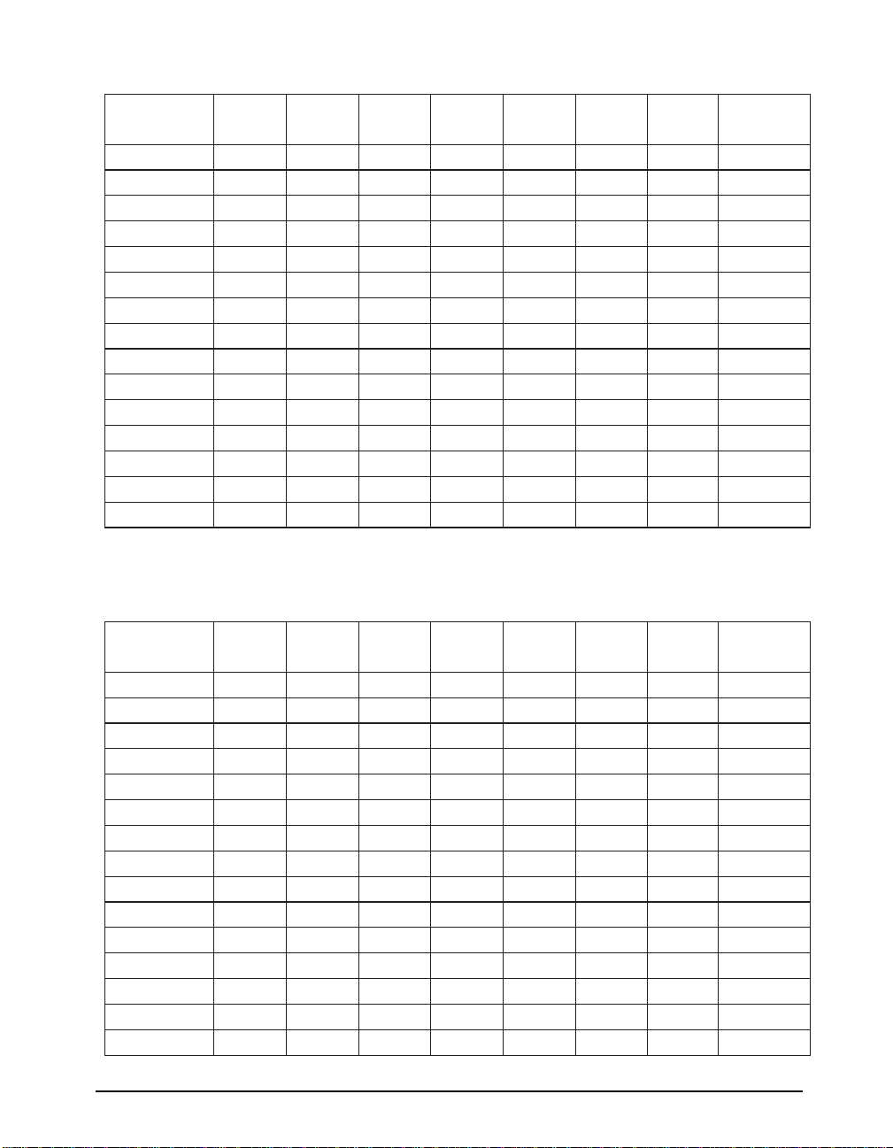
SP3508 Driver Table
tuptuOrevirD
niP
EDOM
T
1
T
1
T
2
T
2
T
3
T
3
T
4
T
4
T
5
T
5
T
6
T
6
T
7
T
8
)2D,1D,0D(
100010110001101011111
)a(TUO53.V11.V82.V11.V11.V11.VZ-hgiH)a(DxT
)b(TUO53.V11.VZ-hgiH11.V11.V11.VZ-hgiH)b(DxT
)a(TUO53.V11.V82.V11.V11.V11.VZ-hgiH)a(ECxT
)b(TUO53.V11.VZ-hgiH11.V11.V11.VZ-hgiH)b(ECxT
)a(TUO53.V11.V82.V11.V11.V11.VZ-hgiH)a(ECD_CxT
)b(TUO53.V11.VZ-hgiH11.V11.V11.VZ-hgiH)b(ECD_CxT
)a(TUO82.V11.V82.V11.V11.V11.VZ-hgiH)a(STR
)b(TUOZ-hgiH11.VZ-hgiH11.V11.V11.VZ-hgiH)b(STR
)a(TUO82.V11.V82.V01.V11.V11.VZ-hgiH)a(RTD
)b(TUOZ-hgiH11.VZ-hgiHZ-hgiH11.V11.VZ-hgiH)b(RTD
)a(TUO82.V11.V82.V11.V11.V11.VZ-hgiH)a(ECD_DCD
)b(TUOZ-hgiH11.VZ-hgiH11.V11.V11.VZ-hgiH)b(ECD_DCD
)a(TUO82.V01.V82.V01.V01.VZ-hgiHZ-hgiHLR
)a(TUO82.V01.V82.V01.V01.VZ-hgiHZ-hgiHLL
Table 1. Driver Mode Selection
edoM53.V
035-AIE
edoM
232-SR
edoM
)82.V(
A035-AIE
edoM
944-SR
edoM
)63.V(
edoM12.X
)11.V(
nwodtuhS
detsegguS
langiS
SP3508 Receiver Table
tupnIrevieceR
niP
EDOM
R
1
R
1
R
2
R
2
R
3
R
3
R
4
R
4
R
5
R
5
R
6
R
6
R
7
R
8
)2D,1D,0D(
)a(NI53.V11.V82.V11.V11.V11.VZ-hgiH)a(DxR
)b(NI53.V11.VZ-hgiH11.V11.V11.VZ-hgiH)b(DxR
)a(NI53.V11.V82.V11.V11.V11.VZ-hgiH)a(CxR
)b(NI53.V11.VZ-hgiH11.V11.V11.VZ-hgiH)b(CxR
)a(NI53.V11.V82.V11.V11.V11.VZ-hgiH)a(ETD_CxT
)b(NI53.V11.VZ-hgiH11.V11.V11.VZ-hgiH)b(ETD_CxT
)a(NI82.V11.V82.V11.V11.V11.VZ-hgiH)a(STC
)b(NIZ-hgiH11.VZ-hgiH11.V11.V11.VZ-hgiH)b(STC
)a(NI82.V11.V82.V01.V11.V11.VZ-hgiH)a(RSD
)b(NIZ-hgiH11.VZ-hgiHZ-hgiH11.V11.VZ-hgiH)b(RSD
)a(NI82.V11.V82.V11.V11.V11.VZ-hgiH)a(ETD_DCD
)b(NIZ-hgiH11.VZ-hgiH11.V11.V11.VZ-hgiH)b(ETD_DCD
)a(NI82.V01.V82.V01.V01.VZ-hgiHZ-hgiHIR
)a(NI82.V01.V82.V01.V01.VZ-hgiHZ-hgiHMT
edoM53.V
100010110001101011111
035-AIE
edoM
232-SR
edoM
)82.V(
A035-AIE
edoM
944-SR
edoM
)63.V(
edoM12.X
)11.V(
nwodtuhS
detsegguS
langiS
Table 2. Receiver Mode Selection
Date: 10/12/04 SP3508 Enhanced WAN Multi–Mode Serial Transceiver © Copyright 2004 Sipex Corporation
11
Page 12
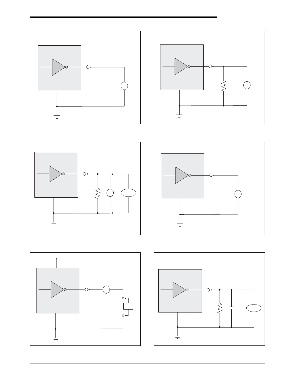
TEST CIRCUITS
A
V
OC
C
C
A
3kΩ
Figure 1. V.28 Driver Output Open Circuit Voltage Figure 2. V.28 Driver Output Loaded Voltage
A
Oscilloscope
7kΩ
C
V
T
Scope used for slew rate
measurement.
C
A
I
sc
V
T
Figure 3. V.28 Driver Output Slew Rate
VCC = 0V
A
C
I
x
Figure 5. V.28 Driver Output Power-Off Impedance
±2V
Figure 4. V.28 Driver Output Short-Circuit Current
A
3kΩ
C
2500pF
Oscilloscope
Figure 6. V.28 Driver Output Rise/Fall Times
Date: 10/12/04 SP3508 Enhanced WAN Multi–Mode Serial Transceiver © Copyright 2004 Sipex Corporation
12
Page 13
A
I
ia
±15V
A
v
oc
C
C
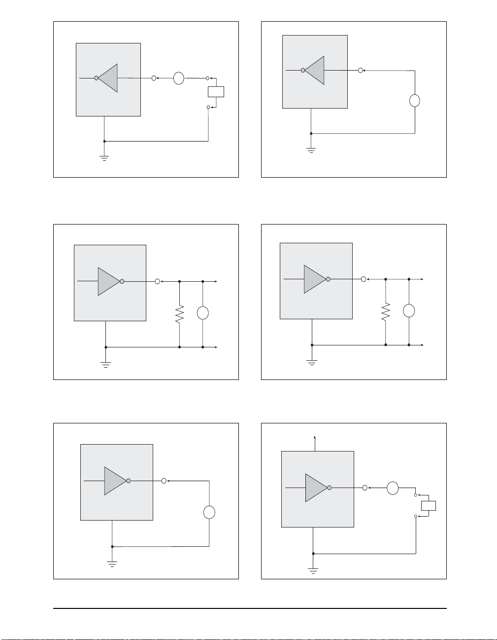
Figure 7. V.28 Receiver Input Impedance Figure 8. V.28 Receiver Input Open Circuit Bias
A
3.9kΩ
V
OC
C
Figure 9. V.10 Driver Output Open-Circuit Voltage
C
Figure 10. V.10 Driver Output Test Terminated Voltage
A
450Ω
V
t
V
= 0V
CC
A
I
sc
C
C
A
I
x
±0.25V
Figure 12. V.10 Driver Output Power-Off CurrentFigure 11. V.10 Driver Output Short-Circuit Current
Date: 10/12/04 SP3508 Enhanced WAN Multi–Mode Serial Transceiver © Copyright 2004 Sipex Corporation
13
Page 14
A
450Ω
Oscilloscope
A
I
ia
±10V
C
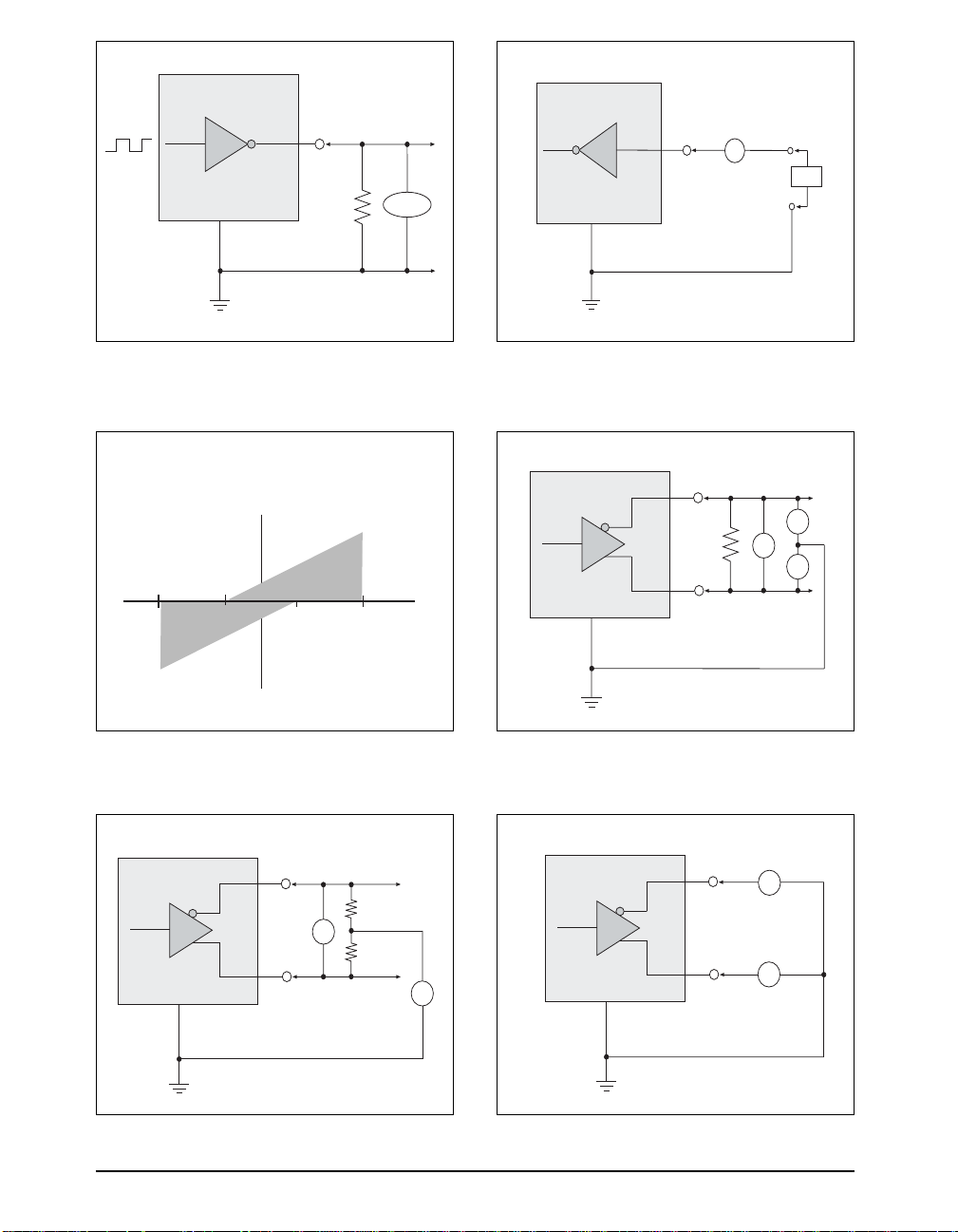
Figure 13. V.10 Driver Output Transition Time
V.10 RECEIVER
+3.25mA
-3V-10V
+3V +10V
Maximum Input Current
Versus Voltage
-3.25mA
Figure 15. V.10 Receiver Input IV Graph
C
Figure 14. V.10 Receiver Input Current
A
V
OCA
3.9kΩ
V
OC
V
OCB
B
C
Figure 16. V.11 Driver Output Open-Circuit Voltage
A
A
I
sa
50Ω
V
T
50Ω
I
sb
B
C
V
OS
C
B
Figure 17. V.11 Driver Output Test Terminated Voltage Figure 18. V.11 Driver Output Short-Circuit Current
Date: 10/12/04 SP3508 Enhanced WAN Multi–Mode Serial Transceiver © Copyright 2004 Sipex Corporation
14
Page 15
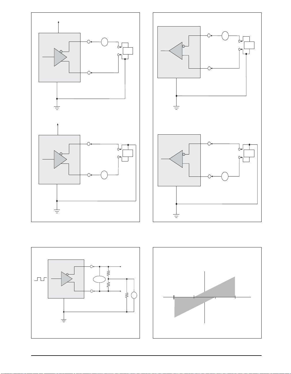
V
= 0V
CC
A
I
A
I
xa
±0.25V
ia
±10V
B
C
V
= 0V
CC
A
I
xb
B
C
Figure 19. V.11 Driver Output Power-Off Current
±0.25V
B
C
A
I
B
C
Figure 20. V.11 Receiver Input Current
±10V
ib
A
50Ω
Oscilloscope
50Ω
B
C
Figure 21. V.11 Driver Output Rise/Fall Time
50Ω
V
E
-3.25mA
Figure 22. V.11 Receiver Input IV Graph
V.11 RECEIVER
-3V-10V
+3.25mA
+3V +10V
Maximum Input Current
Versus Voltage
Date: 10/12/04 SP3508 Enhanced WAN Multi–Mode Serial Transceiver © Copyright 2004 Sipex Corporation
15
Page 16
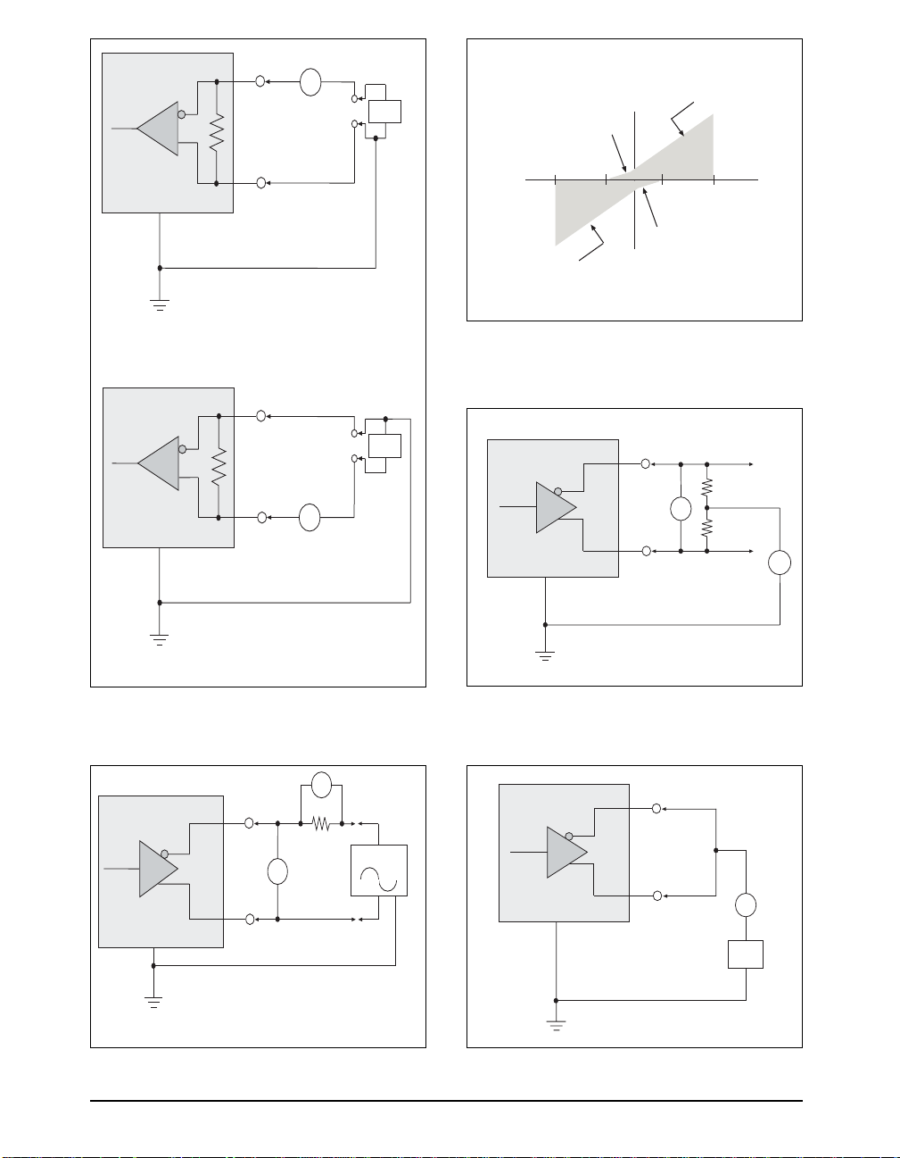
100Ω to
150Ω
A
I
ia
±6V
i [mA] = V [V] - 3) / 4.0
B
V.11 RECEIVER
w/ Optional Cable Termination
(100Ω to 150Ω)
-6V
-3V
i [mA] = V [V] / 0.1
+3V +6V
i [mA] = V [V] - 3) / 4.0
C
i [mA] = V [V] / 0.1
Maximum Input Current
versus Voltage
Figure 24. V.11 Receiver Input Graph with Termination
A
100Ω to
150Ω
I
ib
B
±6V
C
Figure 23. V.11 Receiver Input Current w/ Termination
V
1
A
50Ω
24kHz, 550mV
p-p
V
2
B
C
Sine Wave
A
50Ω
V
T
50Ω
B
C
V
OS
Figure 25. V.35 Driver Output Test Terminated Voltage
A
I
B
C
SC
±2V
Figure 26. V.35 Driver Output Source Impedance
Figure 27. V.35 Driver Output Short-Circuit Impedance
Date: 10/12/04 SP3508 Enhanced WAN Multi–Mode Serial Transceiver © Copyright 2004 Sipex Corporation
16
Page 17
V
A
1
A
50Ω
Oscilloscope
50Ω
50Ω
24kHz, 550mV
p-p
V
2
Sine Wave
B
50Ω
C
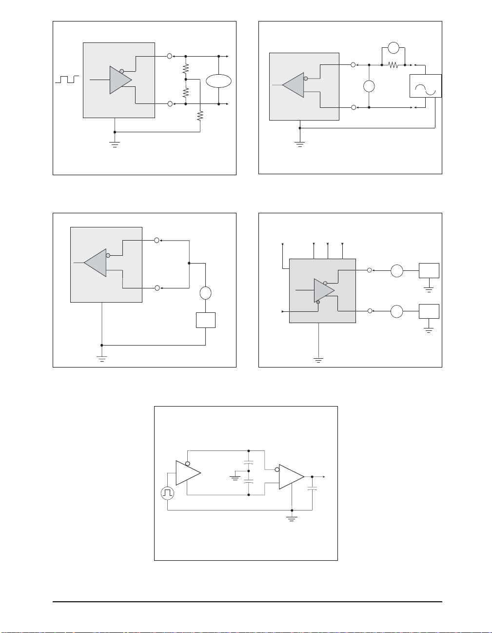
Figure 28. V.35 Driver Output Rise/Fall Time
A
I
B
sc
±2V
C
Figure 30. V.35 Receiver Input Short-Circuit Impedance
B
C
Figure 29. V.35 Receiver Input Source Impedance
Any one of the three conditions for disabling the driver.
V
CC
11 1
D
D
D
0
1
2
A
I
ZSC
I
ZSC
B
VCC = 0V
Logic “1”
Figure 31. Driver Output Leakage Current Test
±10V
±10V
T
IN
f
IN
B
A
(50% Duty Cycle, 2.5V
L1
C
L2
)
P-P
B
A
R
OUT
15pF
C
Figure 32. Driver/Receiver Timing Test Circuit
Date: 10/12/04 SP3508 Enhanced WAN Multi–Mode Serial Transceiver © Copyright 2004 Sipex Corporation
17
Page 18
Output
Under
Test
V
S
500Ω
C
L
1
S
2
CC
Receiver
Output
Test Point
RL
1KΩC
1KΩ
V
S
1
S
2
CC
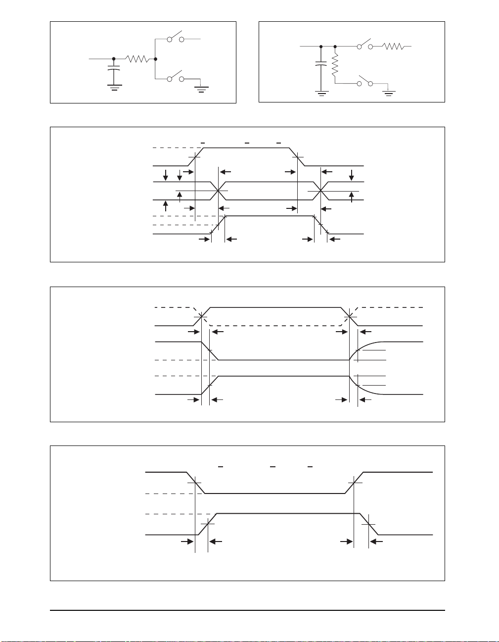
Figure 33. Driver Timing Test Load Circuit
B
– V
+3V
0V
A
1/2V
V
O
B
+
V
O
0V
–
V
O
A
|
DRIVER
INPUT
DRIVER
OUTPUT
DIFFERENTIAL
OUTPUT
V
t
SKEW = | tDPLH - tDPHL
Figure 35. Driver Propagation Delays
Mx or Tx_Enable
+3V
0V
5V
A, B
V
OL
V
OH
A, B
0V
Figure 34. Receiver Timing Test Load Circuit
f > 10MHz; tR < 5ns; tF < 5ns
1.5V 1.5V
O
t
PLH
t
DPLH
f = 1MHz; t
t
R
t
PHL
t
DPHL
≤ 10ns; tF ≤ 10ns
R
1.5V 1.5V
t
ZL
2.3V
2.3V
Output normally LOW
Output normally HIGH
t
ZH
t
F
1/2V
O
0.5V
0.5V
t
LZ
t
HZ
Figure 36. Driver Enable and Disable Times
f > 10MHz; tR < 5ns; tF < 5ns
+
V
A – B
RECEIVER OUT
t
SKEW
= |
t
PHL
0D2
–
V
0D2
V
OH
V
OL
t
-
PLH
t
PLH
|
0V 0V
INPUT
OUTPUT
(VOH - VOL)/2
t
PHL
(V
OH
- VOL)/2
Figure 37. Receiver Propagation Delays
Date: 10/12/04 SP3508 Enhanced WAN Multi–Mode Serial Transceiver © Copyright 2004 Sipex Corporation
18
Page 19
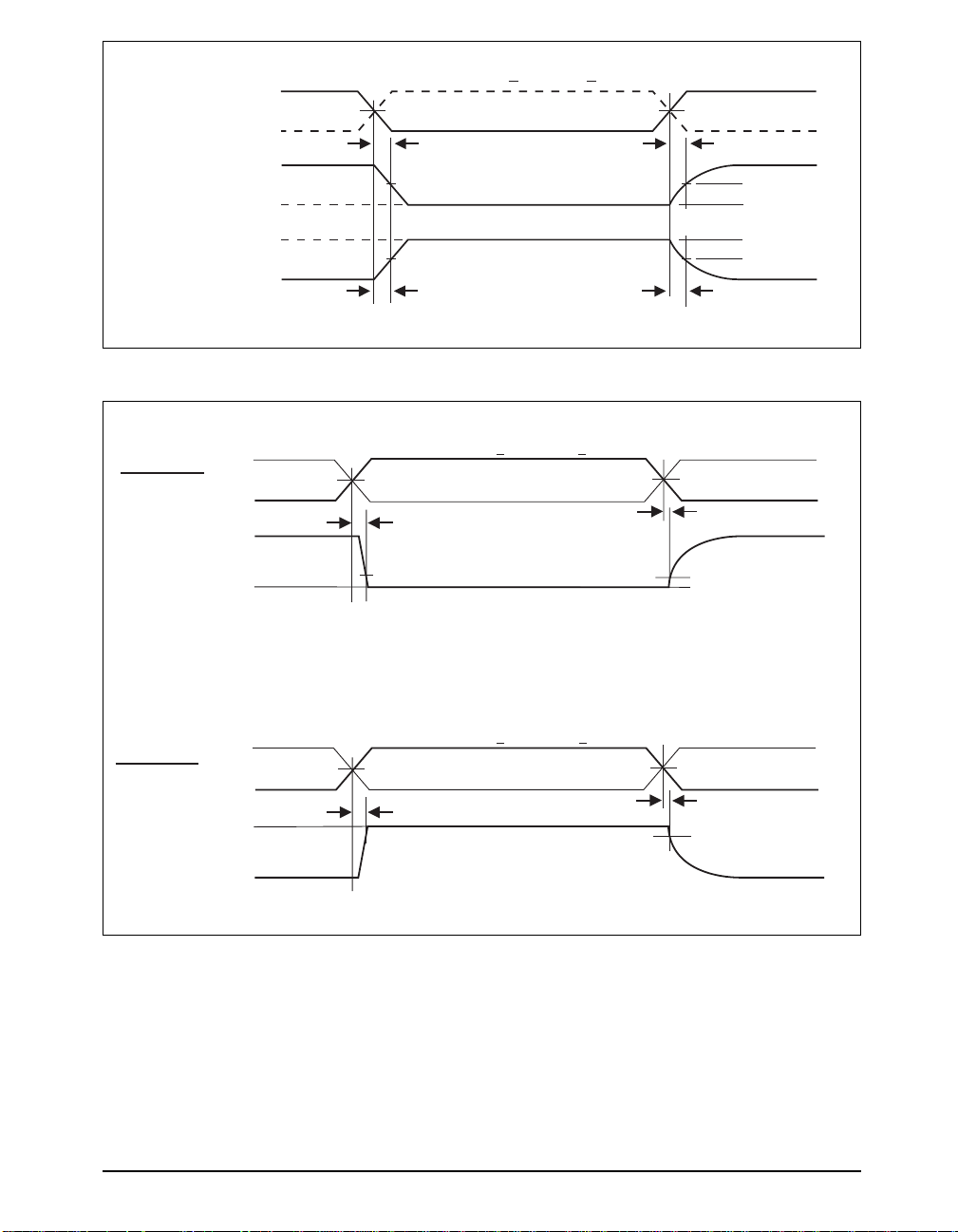
+3V
DECx
RxENABLE
0V
+3.3V
RECEIVER OUT
V
IL
V
IH
RECEIVER OUT
0V
Figure 38. Receiver Enable and Disable Times
f = 1MHz; tR < 10ns; tF < 10ns
1.5V 1.5V
t
ZL
1.5V
1.5V
Output normally LOW
Output normally HIGH
t
ZH
0.5V
0.5V
t
LZ
t
HZ
+3V
f = 60kHz; tR < 10ns; tF < 10ns
Tx_Enable
1.5V
0V
t
ZL
V
0.5V
-
OL
Output LOW
T
OUT
V
0V
OL
f = 60kHz; tR < 10ns; tF < 10ns
+3V
Tx_Enable
1.5V
0V
t
T
OUT
V
OH
ZH
Output HIGH
0V
Figure 39. V.28 (RS-232) and V.10 (RS-423) Driver Enable and Disable Times
1.5V
t
V
1.5V
V
OL
t
LZ
HZ
OH
0.5V
-
-
0.5V
Date: 10/12/04 SP3508 Enhanced WAN Multi–Mode Serial Transceiver © Copyright 2004 Sipex Corporation
19
Page 20
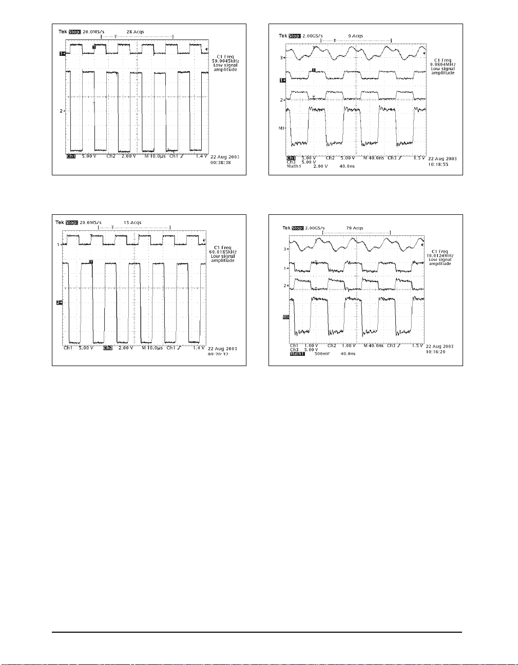
Figure 40. Typical V.10 Driver Output Waveform. Figure 41. Typical V.11 Driver Output Waveform.
Figure 42. Typical V.28 Driver Output Waveform.
Date: 10/12/04 SP3508 Enhanced WAN Multi–Mode Serial Transceiver © Copyright 2004 Sipex Corporation
Figure 43. Typical V.35 Driver Output Waveform.
20
Page 21
(S
ee pinout assignments for
GND and V
RECEIVER TERMINATION NETWORK
V.35 MODE
V.11 MODE
RX ENABLE
RD(a)
RD(b)
RT(a)
RT(b)
TxC(a)
TxC(b)
CS(a)
CS(b)
DM(a)
DM(b)
RRT(a)
RRT(b)
TM(a)
51ohms
51ohms
IC
124ohms
pins)
CC
TxCEN
DCD_DTE
RRTEN
RxD
RDEN
RxC
RTEN
TxC
CTS
CSEN
DSR
DMEN
ICEN
TMEN
+3.3V
RI
TM
+3.3V
(decoupling capacitor not shown)
C
VDD
1µF
76
29
50
39
10
49
52
40
11
51
55
41
12
53
57
42
13
56
59
43
14
58
62
44
15
61
63
45
16
64
46
17
18
19
20
21
22
30
V
DD
AV
CC
D0
D1
D2
D-LATCH
TERM-OFF
LOOPBACK
V
CC
1µF
74
Regulated Charge Pump
Inverter
SP3508
GND
C1
C2
1µF
69
72
70
C1-C1+
C2-C2+
V.10-GND
AGND
24
C3+
26
C3-
V
SS1
27
V
SS2
C3
1µF
68
1µF
C
VSS1
C
VSS2
1µF
31
97
99
2
32
93
95
3
33
89
91
4
34
81
83
5
35
85
87
6
36
79
77
7
37
67
8
38
65
9
60
28
TxD
SD(a)
SD(b)
SDEN
TxCE
TT(a)
TT(b)
TTEN
ST
ST(a)
ST(b)
STEN
RTS
RS(a)
RS(b)
RSEN
DTR
TR(a)
TR(b)
TREN
DCD_DCE
RRC(a)
RRC(b)
RRCEN
RL
RL(a)
RLEN
LL
LL(a)
LLEN
V.35 DRIVER TERMINATION NETWORK
51ohms
V.35 MODE
TX ENABLE
124ohms
51ohms
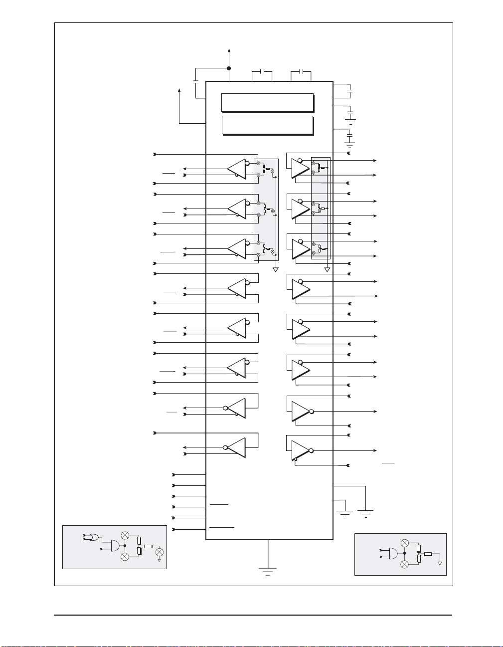
Figure 44. Functional Diagram
Date: 10/12/04 SP3508 Enhanced WAN Multi–Mode Serial Transceiver © Copyright 2004 Sipex Corporation
21
Page 22

The SP3508 contains highly integrated serial
transceivers that offer programmability between
interface modes through software control. The
SP3508 offers the hardware interface modes for
RS-232 (V.28), RS-449/V.36 (V.11 and V.10),
EIA-530 (V.11 and V.10), EIA-530A (V.11 and
V.10), V.35 (V.35 and V.28) and X.21(V.11).
The interface mode selection is done via three
control pins, which can be latched via microprocessor control.
The SP3508 has eight drivers, eight receivers,
and Sipex's patented on-board charge pump
(5,306,954) that is ideally suited for wide area
network connectivity and other multi-protocol
applications. Other features include digital and
line loopback modes, individual enable/disable
control lines for each driver and receiver, failsafe when inputs are either open or shorted.
THEORY OF OPERATION
The SP3508 device is made up of
1) the drivers
2) the receivers
3) charge pumps
4) DTE/DCE switching algorithm
5) control logic.
Drivers
The SP3508 has eight enhanced independent
drivers. Control for the mode selection is done
via a three-bit control word into D0, D1, and D2.
The drivers are prearranged such that for each
mode of operation, the relative position and
functionality of the drivers are set up to accommodate the selected interface mode. As the
mode of the drivers is changed, the electrical
characteristics will change to support the required signal levels. The mode of each driver in
the different interface modes that can be selected is shown in Table 1.
FEATURES
There are four basic types of driver circuits –
ITU-T-V.28 (RS-232), ITU-T-V.10 (RS-423),
ITU-T-V.11 (RS-422), and CCITT-V.35.
The V.28 (RS-232) drivers output single-ended
signals with a minimum of
+5V (with 3kΩ &
2500pF loading), and can operate over 120kbps.
Since the SP3508 uses a charge pump to generate the RS-232 output rails, the driver outputs
will never exceed
+10V. The V.28 driver architecture is similar to Sipex's standard line of RS232 transceivers.
The RS-423 (V.10) drivers are also single-ended
signals which produce open circuit VOL and
VOH measurements of +4.0V to +6.0V. When
terminated with a 450Ω load to ground, the
driver output will not deviate more than 10% of
the open circuit value. This is in compliance of
the ITU V.10 specification. The V.10 (RS-423)
drivers are used in RS-449/V.36, EIA-530, and
EIA-530A modes as Category II signals from
each of their corresponding specifications. The
V.10 driver can transmit over 120Kbps if necessary.
The third type of drivers are V.11 (RS-422)
differential drivers. Due to the nature of differential signaling, the drivers are more immune to
noise as opposed to single-ended transmission
methods. The advantage is evident over high
speeds and long transmission lines. The strength
of the driver outputs can produce differential
signals that can maintain +2V differential output levels with a load of 100Ω. The strength
allows the SP3508 differential driver to drive
over long cable lengths with minimal signal
degradation. The V.11 drivers are used in RS449, EIA-530, EIA-530A and V.36 modes as
Category I signals which are used for clock and
data. Sipex's new driver design over its predecessors allow the SP3508 to operate over 20Mbps
for differential transmission.
Date: 10/12/04 SP3508 Enhanced WAN Multi–Mode Serial Transceiver © Copyright 2004 Sipex Corporation
22
Page 23

FEATURES
The fourth type of drivers are V.35 differential
drivers.
There are only three available on the
SP3508 for data and clock (TxD, TxCE, and TxC
in DCE mode). These drivers are current sources
that drive loop current through a differential pair
resulting in a 550mV differential voltage at the
receiver. These drivers also incorporate fixed
termination networks for each driver in order to
set the VOH and VOL depending on load conditions.
This termination network is basically a “Y”
configuration consisting of two 51Ω resistors
connected in series and a 124Ω resistor connected
between the two 50Ω resistors to GND. Filtering
can be done on these pins to reduce common
mode noise transmitted over the transmission
line by connecting a capacitor to ground.
The drivers also have separate enable pins
which simplifies half-duplex configurations for
some applications, especially programmable
DTE/DCE. The enable pins will either enable or
disable the output of the drivers according to the
appropriate active logic illustrated on Figure 44.
The enable pins have internal pull-up and pulldown devices, depending on the active polarity
of the receiver, that enable the driver upon poweron if the enable lines are left floating. During
disabled conditions, the driver outputs will be at
a high impedance 3-state.
The driver inputs are both TTL or CMOS
compatible. All driver inputs have an internal
pull-up resistor so that the output will be at a
defined state at logic LOW (“0”). Unused driver
inputs can be left floating. The internal pull-up
resistor value is approximately 500kΩ.
Receivers
The SP3508 has eight enhanced independent
receivers. Control for the mode selection is done
via a three-bit control word that is the same as the
driver control word. Therefore, the modes for
the drivers and receivers are identical in the
application.
Like the drivers, the receivers are prearranged
for the specific requirements of the synchronous
serial interface. As the operating mode of the
receivers is changed, the electrical characteristics
will change to support the required serial interface
protocols of the receivers. Table 1 shows
the mode of each receiver in the different
interface modes that can be selected. There are
two basic types of receiver circuits—ITU-T-V .28
(RS-232) and ITU-T-V.11, (RS-422).
The RS-232 (V.28) receiver is single-ended and
accepts RS-232 signals from the RS-232 driver.
The RS-232 receiver has an operating input
voltage range of +15V and can receive signals
downs to +3V. The input sensitivity complies
with RS-232 and V.28 at +3V. The input
impedance is 3kΩ to 7kΩ in accordance to RS232 and V.28. The receiver output produces a
TTL/CMOS signal with a +2.4V minimum for
a logic “1” and a +0.4V maximum for a logic “0”.
The RS-232 (V.28) protocol uses these receivers
for all data, clock and control signals. They are
also used in V.35 mode for control line signals:
CTS, DSR, LL, and RL. The RS-232 receivers
can operate over 120kbps.
The second type of receiver is a differential type
that can be configured internally to support
ITU-T-V.10 and CCITT-V.35 depending on its
input conditions. This receiver has a typical
input impedance of 10kΩ and a differential
threshold of less than +200mV, which complies
with the ITU-T-V.11 (RS-422) specifications.
V.11 receivers are used in RS-449/V.36,
EIA-530, EIA-530A and X.21 as Category I
signals for receiving clock, data, and some control
line signals not covered by Category II V.10
circuits. The differential V.11 transceiver has
improved architecture that allows over 20Mbps
transmission rates.
Receivers dedicated for data and clock (RxD,
RxC, TxC) incorporate internal termination for
V.11. The termination resistor is typically 120Ω
connected between the A and B inputs. The
termination is essential for minimizing crosstalk
and signal reflection over the transmission line .
The minimum value is guaranteed to exceed
100Ω, thus complying with the V.11 and RS-422
specifications. This resistor is invoked when the
receiver is operating as a V.11 receiver, in modes
EIA-530, EIA-530A, RS-449/V.36, and X.21.
Date: 10/12/04 SP3508 Enhanced WAN Multi–Mode Serial Transceiver © Copyright 2004 Sipex Corporation
23
Page 24
FEATURES
The same receivers also incorporate a termination
network internally for V.35 applications. For
V.35, the receiver input termination is a “Y”
termination consisting of two 51Ω resistors
connected in series and a 124Ω resistor connected
between the two 50Ω resistors and GND. The
receiver itself is identical to the V.11 receiver.
The differential receivers can be configured to
be ITU-T-V.10 single-ended receivers by
internally connecting the non-inverting input to
ground. This is internally done by default from
the decoder. The non-inverting input is rerouted
to V10GND and can be grounded separately.
The ITU-T-V.10 receivers can operate over
120Kbps and are used in RS-449/V.36, E1A530, E1A-530A and X.21 modes as Category II
signals as indicated by their corresponding
specifications. All receivers include an enable/
disable line for disabling the receiver output
allowing convenient half-duplex configurations.
The enable pins will either enable or disable the
output of the receivers according to the
appropriate active logic illustrated on Figure 44.
The receiver’s enable lines include an internal
pull-up or pull-down device, depending on the
active polarity of the receiver, that enables the
receiver upon power up if the enable lines are left
floating. During disabled conditions, the receiver
outputs will be at a high impedance state. If the
receiver is disabled any associated termination is
also disconnected from the inputs.
All receivers include a fail-safe feature that
outputs a logic high when the receiver inputs are
open, terminated but open, or shorted together.
For single-ended V.28 and V.10 receivers, there
are internal 5kΩ pull-down resistors on the inputs
which produces a logic high (“1”) at the receiver
outputs. The differential receivers have a
proprietary circuit that detect open or shorted
inputs and if so, will produce a logic HIGH (“1”)
at the receiver output.
CHARGE PUMP
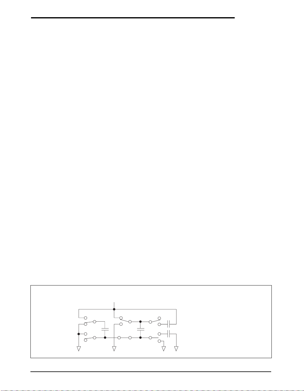
SP3508 uses an internal capacitive charge pump
to generate Vdd and Vss. The design is Sipex
patented (5,306,954) four-phased voltage shifting charge pump converters that converts the
input voltage of 3.3V to nominal output voltages of +/-6V (Vdd & Vss1). SP3508 also includes an inverter block that inverts Vcc to -Vcc
(Vss2). There is a free-running oscillator that
controls the four phases of the voltage shifting.
A description of each phase follows.
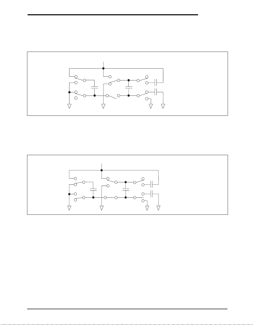
4-phased doubler pump
Phase 1
-V
charge storage -During this phase of the
SS1
clock cycle, the positive side of capacitors C1
and C2 are initially charged to VCC. C1+ is then
switched to ground and the charge in C1- is
transferred to C2-. Since C2+ is connected to
VCC, the voltage potential across capacitor C2 is
now 2xVCC.
VCC = +3V
C
+3V
++
C
1
–3V –3V
Figure 45. Charge Pump - Phase 1.
Date: 10/12/04 SP3508 Enhanced WAN Multi–Mode Serial Transceiver © Copyright 2004 Sipex Corporation
C
2
––
+
–
C
VDD
+
VSS1
–
V
V
Storage Capacitor
DD
Storage Capacitor
SS1
24
Page 25
FEATURES
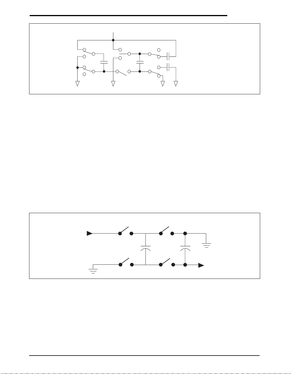
Phase 2
-V
transfer -Phase two of the clock connects the negative terminal of C2 to the V
SS1
and the positive terminal of C2 to ground, and transfers the negative generated voltage to C
storage capacitor
SS1
VSS1
. This
generated voltage is regulated to -5.5V. Simultaneously, the positive side of the capacitor C1 is switched
to VCC and the negative side is connected to ground.
VCC = +3V
C
VDD
+
–
Storage Capacitor
V
+
VSS1
DD
Storage Capacitor
V
SS
Figure 46. Charge Pump - Phase 2.
++
C
1
C
2
––
–6V
–
C
Phase 3
-VDD charge storage -The third phase of the clock is identical to the first phase-the charge transferred in
C1 produces -VCC in the negative terminal of C1 which is applied to the negative side of the capacitor C2.
Since C2+ is at VCC, the voltage potential across C2 is 2xVCC.
VCC = +3V
C
+
–
C
VDD
–
+
VSS1
Storage Capacitor
V
DD
Storage Capacitor
V
SS1
Figure 47.Charge Pump - Phase 3.
+3V
++
C
1
–3V
C
2
––
–3V
Phase 4
-VDD transfer -The fourth phase of the clock connects the negative terminal of C2 to ground, and transfers
the generated 5.5V across C2 to C
, the VDD storage capacitor. This voltage is regulated to +5.5V. At
VDD
the regulated voltage, the internal oscillator is disabled and simultaneously with this, the positive side of
capacitor C1 is switched to VCC and the negative side is connected to ground, and the cycle begins again.
The charge pump cycle will continue as long as the operational conditions for the internal oscillator are
present. Since both V+ and V- are separately generated from VCC; in a no-load condition V+ and V- will
be symmetrical. Older charge pump approaches that generate V- from V+ will show a decrease in the
magnitude of
V- compared to V+ due to the inherent inefficiencies in the design. The clock rate for the charge pump
typically operates at 250kHz. The external capacitors can be as low as 1µF with a 16V breakdown voltage
rating.
Date: 10/12/04 SP3508 Enhanced WAN Multi–Mode Serial Transceiver © Copyright 2004 Sipex Corporation
25
Page 26
FEATURES
VCC = +3V
C
+
–
C
VDD
VSS1
–
Storage Capacitor
V
DD
+
Storage Capacitor
V
SS1
Figure 48. Charge Pump - Phase 4.
+6V
++
C
1
C
2
––
2-phased inverter pump
Phase 1
Please refer to figure below: In the first phase of the clock cycle, switches S2 and S4 are opened and S1 and
S3 closed. This connects the flying capacitor, C3, from Vin to ground. C3 charge up to the input voltage
applied at Vcc.
Phase 2
In the second phase of the clock cycle, switches S2 and S4 are closed and S1 and S3 are opened. This
connects the flying capacitor, C3, in parallel with the output capacitor, C
now transferred to C
side is connected to ground. With the voltage across C
flows from C3 to C
. Simultaneously, the negative side of C
VSS2
until the voltage at the V
VSS2
equals -VCC.
SS2
is connected to V
VSS2
smaller than the voltage across C3, the charge
VSS2
. The Charge stored in C3 is
VSS2
and the positive
SS2
V
= -V
SS2
V
CC
S
1
C
S
3
Figure 49. Circuit for an Ideal Voltage Inverter.
Date: 10/12/04 SP3508 Enhanced WAN Multi–Mode Serial Transceiver © Copyright 2004 Sipex Corporation
CC
S
+
3
2
S
4
+
C
VSS2
V
SS2
26
Page 27
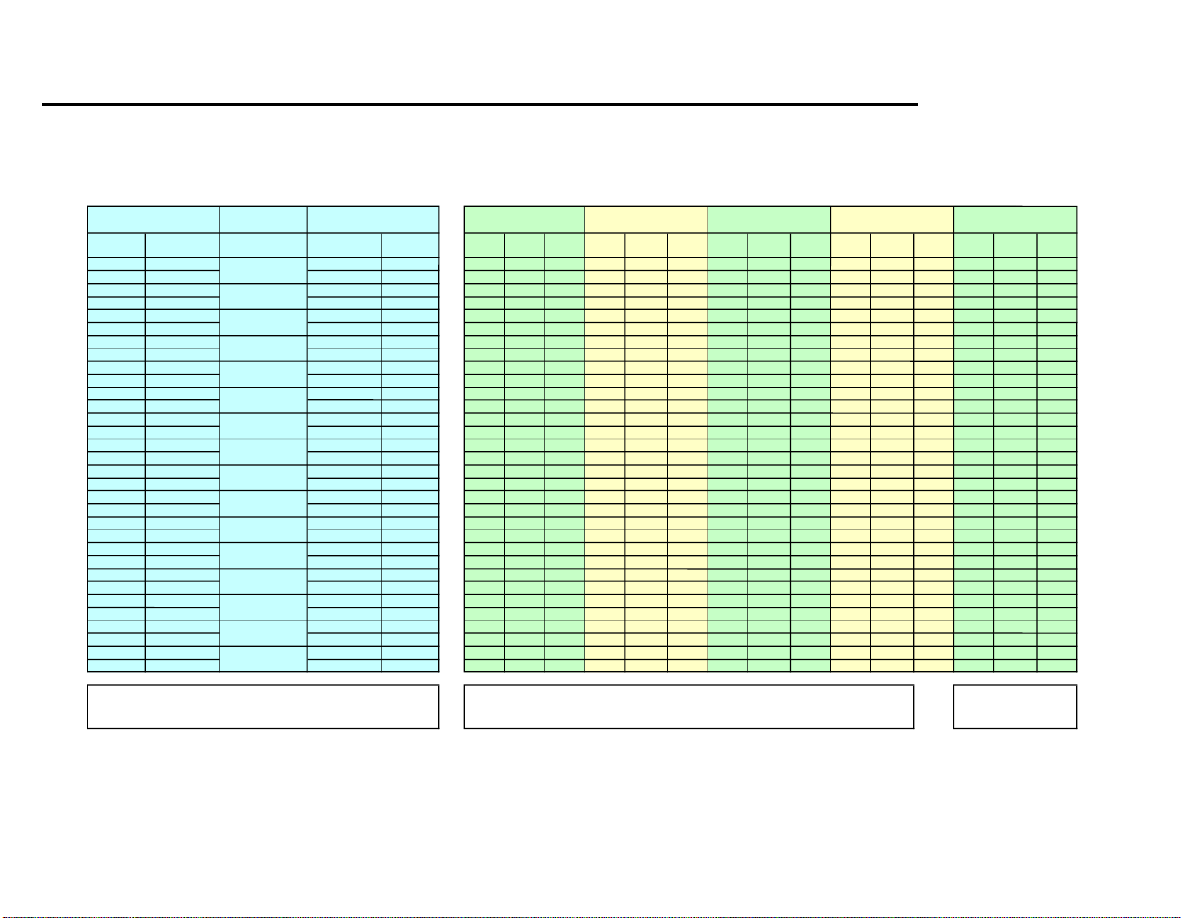
Recommended Signals and Port Pin Assignments
Pin
Number
Pin Mnemonic Circuit Pin Mnemonic
Pin
Number
Signal
Type
Mnemo
nic
DB-25
Pin(F)
Signal
Type
Mnemo
nic
DB-25
Pin(F)
Signal
Type
Mnemo
nic
DB-37
Pin(F)
Signal
Type
Mnemo
nic
M34
Pin(F)
Signal
Type
Mnemo
nic
DB-15
Pin(F)
31 TxD SD(A) 97 V.28 BB 3 V.11 BB(A) 3 V.11 RD(A) 6 V.35 104 R V.11 R(A) 4
2 SDEN SD(B) 99 V.11 BB(B) 16 V.11 RD(B) 24 V.35 104 T V.11 R(B) 11
32 TxCE TT(A) 93 V.28 DD 17 V.11 DD(A) 17 V.11 RT(A) 8 V.35 115 V V.11 B(A) 7**
3 TTEN TT(B) 95 V.11 DD(B) 9 V.11 RT(B) 26 V.35 115 X V.11 B(B) 14**
33 ST ST(A) 89 V.28 DB 15 V.11 DB(A) 15 V.11 ST(A) 5 V.35 114 Y V.11 S(A) 6
4 STEN ST(B) 91 V.11 DB(B) 12 V.11 ST(B) 23 V.35 114 AA V.11 S(B) 13
34 RTS RS(A) 81 V.28 CB 5 V.11 CB(A) 5 V.11 CS(A) 9 V.28 106 D V.11 I(A) 5
5 RSEN RS(B) 83 V.11 CB(B) 13 V.11 CS(B) 27 V.11 I(B) 12
35 DTR TR(A) 85 V.28 CC 6 V.11 CC(A) 6 V.11 DM(A) 11 V.28 107 E
6 TREN TR(B) 87 V.11 CC(B) 22 V.11 DM(B) 29
36 DCD_DCE RRC(A) 79 V.28 CF 8 V.11 CF(A) 8 V.11 RR(A) 13 V.28 109 F
7 RRCEN RRC(B) 77 V.11 CF(B) 10 V.11 RR(B) 31
37 RL RL(A) 67 V.28 CE 22 V.28 125 J
8RLEN
38 LL LL(A) 65 V.28 TM 25 V.10 TM 25 V.10 TM 18 V.28 142 NN
9 LLEN#
39 RxD RD(A) 50 V.28 BA 2 V.11 BA(A) 2 V.11 SD(A) 4 V.35 103 P V.11 T(A) 2
10 RDEN# RD(B) 49 V.11 BA(B) 12 V.11 SD(B) 22 V.35 103 S V.11 T(B) 9
40 RxC RT(A) 52 V.28 DA 24 V.11 DA(A) 24 V.11 TT(A) 17 V.35 113 U V.11 X(A) 7**
11 RTEN# RT(B) 51 V.11 DA(B) 11 V.11 TT(B) 35 V.35 113 W V.11 X(B) 14**
41 TxC TxC(A) 55
12 TxCEN# TxC(B) 53
42 CTS CS(A) 57 V.28 CA 4 V.11 CA(A) 4 V.11 RS(A) 7 V.28 105 C V.11 C(A) 3
13 CSEN# CS(B) 56 V.11 CA(B) 19 V.11 RS(B) 25 V.11 C(B) 10
43 DSR DM(A) 59 V.28 CD 20 V.11 CD(A) 20 V.11 TR(A) 12 V.28 108 H
14 DMEN# DM(B) 58 V.11 CD(B) 23 V.11 TR(B) 30
44 DCD_DTE RRT(A) 62
15 RRTEN# RRT(B) 61
45 RI IC 63 V.28 RL 21 V.10 RL 21 V.10 RL 14 V.28 140 N
16 ICEN#
46 TM TM(A) 64 V.28 LL 18 V.10 LL 18 V.10 LL 10 V.28 141 L
17 TMEN
SP3508 Multiprotocol Configured as DCE
Interface to System Logic
Interface to Port-
Connector
Receiver_4
Receiver_5
Receiver_6
Driver_7
Driver_8
RS-449
V.35
X.21
Driver_1
RS-232 or V.24
EIA-530
Receiver_2
Receiver_3
Driver_2
Driver_3
Driver_4
Driver_5
Receiver_1
Driver_6
Spare drivers and receivers may be used for optional signals (Signal
Quality, Rate Detect, Standby) or may be disabled using individual
enable pins for each driver and receiver
** X.21 use either B() or
X(), not both
Pin assignments and signal functions are subject to national or regional variation and
proprietary / non-standard implementations
Receiver_7
Receiver_8
DCE CONFIGURATION
Date: 06/14/04 SP3508 Enhanced WAN Multi–Mode Serial Transceiver © Copyright 2004 Sipex Corporation
27
27
Date: 10/12/04 SP3508 Enhanced WAN Multi–Mode Serial Transceiver © Copyright 2004 Sipex Corporation
Page 28
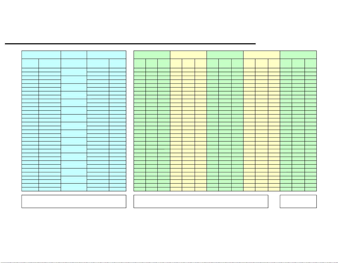
Recommended Signals and Port Pin Assignments
Pin
Number
Pin Mnemonic Circuit Pin Mnemonic
Pin
Number
Signal
Type
Mnemo
nic
DB-25
Pin(M)
Signal
Type
Mnemo
nic
DB-25
Pin(M)
Signal
Type
Mnemo
nic
DB-37
Pin(M)
Signal
Type
Mnemo
nic
M34
Pin(M)
Signal
Type
Mnemo
nic
DB-15
Pin(M)
31 TxD SD(A) 97 V.28 BA 2 V.11 BA(A) 2 V.11 SD(A) 4 V.35 103 P V.11 T(A) 2
2 SDEN SD(B) 99 V.11 BA(B) 12 V.11 SD(B) 22 V.35 103 S V.11 T(B) 9
32 TxCE TT(A) 93 V.28 DA 24 V.11 DA(A) 24 V.11 TT(A) 17 V.35 113 U V.11 X(A) 7**
3 TTEN TT(B) 95 V.11 DA(B) 11 V.11 TT(B) 35 V.35 113 W V.11 X(B) 14**
33 ST ST(A) 89
4 STEN ST(B) 91
34 RTS RS(A) 81 V.28 CA 4 V.11 CA(A) 4 V.11 RS(A) 7 V.28 105 C V.11 C(A) 3
5 RSEN RS(B) 83 V.11 CA(B) 19 V.11 RS(B) 25 V.11 C(B) 10
35 DTR TR(A) 85 V.28 CD 20 V.11 CD(A) 20 V.11 TR(A) 12 V.28 108 H
6 TREN TR(B) 87 V.11 CD(B) 23 V.11 TR(B) 30
36 DCD_DCE RRC(A) 79
7 RRCEN RRC(B) 77
37 RL RL(A) 67 V.28 RL 21 V.10 RL 21 V.10 RL 14 V.28 140 N
8RLEN
38 LL LL(A) 65 V.28 LL 18 V.10 LL 18 V.10 LL 10 V.28 141 L
9LLEN#
39 RxD RD(A) 50 V.28 BB 3 V.11 BB(A) 3 V.11 RD(A) 6 V.35 104 R V.11 R(A) 4
10 RDEN# RD(B) 49 V.11 BB(B) 16 V.11 RD(B) 24 V.35 104 T V.11 R(B) 11
40 RxC RT(A) 52 V.28 DD 17 V.11 DD(A) 17 V.11 RT(A) 8 V.35 115 V V.11 B(A) 7**
11 RTEN# RT(B) 51 V.11 DD(B) 9 V.11 RT(B) 26 V.35 115 X V.11 B(B) 14**
41 TxC TxC(A) 55 V.28 DB 15 V.11 DB(A) 15 V.11 ST(A) 5 V.35 114 Y V.11 S(A) 6
12 TxCEN# TxC(B) 53 V.11 DB(B) 12 V.11 ST(B) 23 V.35 114 AA V.11 S(B) 13
42 CTS CS(A) 57 V.28 CB 5 V.11 CB(A) 5 V.11 CS(A) 9 V.28 106 D V.11 I(A) 5
13 CSEN# CS(B) 56 V.11 CB(B) 13 V.11 CS(B) 27 V.11 I(B) 12
43 DSR DM(A) 59 V.28 CC 6 V.11 CC(A) 6 V.11 DM(A) 11 V.28 107 E
14 DMEN# DM(B) 58 V.11 CC(B) 22 V.11 DM(B) 29
44 DCD_DTE RRT(A) 62 V.28 CF 8 V.11 CF(A) 8 V.11 RR(A) 13 V.28 109 F
15 RRTEN# RRT(B) 61 V.11 CF(B) 10 V.11 RR(B) 31
45 RI IC 63 V.28 CE 22 V.28 125 J
16 ICEN#
46 TM TM(A) 64 V.28 TM 25 V.10 TM 25 V.10 TM 18 V.28 142 NN
17 TMEN
RS-449
V.35
X.21
Receiver_7
Receiver_8
RS-232 or V.24
EIA-530
Receiver_4
Receiver_5
Receiver_6
Driver_7
Driver_8
Driver_6
Driver_2
Driver_3
Driver_4
Driver_5
Spare drivers and receivers may be used for optional signals (Signal
Quality, Rate Detect, Standby) or may be disabled using individual
enable pins for each driver and receiver
** X.21 use either B() or
X(), not both
Pin assignments and signal functions are subject to national or regional variation and
proprietary / non-standard implementations
SP3508 Multiprotocol Configured as DTE
Interface to System Logic
Interface to Port-
Connector
Driver_1
Receiver_1
Receiver_2
Receiver_3
DTE CONFIGURATION
Date: 06/14/04 SP3508 Enhanced WAN Multi–Mode Serial Transceiver © Copyright 2004 Sipex Corporation
28
28
Date: 10/12/04 SP3508 Enhanced WAN Multi–Mode Serial Transceiver © Copyright 2004 Sipex Corporation
Page 29

TERM_OFF FUNCTION
The SP3508 contains a TERM_OFF pin that disables all three receiver input termination networks
regardless of mode. This allows the device to be
used in monitor mode applications typically found
in networking test equipment.
The TERM_OFF pin internally contains a pulldown device with an impedance of over 500kΩ,
which will default in a "ON" condition during
power-up if V.35 receivers enable line and the
SHUTDOWN mode from the decoder will disable
the termination regardless of TERM_OFF.
LOOPBACK FUNCTION
The SP3508 contains a LOOPBACK pin that
invokes a loopback path. This loopback path is
illustrated in Figure 50. LOOPBACK has an internal pull-up resistor that defaults to normal mode
during power up or if the pin is left floating. During
loopback, the driver output and receiver input
characteristics will still adhere to its appropriate
specifications.
FEATURES
There are internal pull-up devices on D0, D1 and
D2, which allow the device to be in SHUTDOWN
mode ("111") upon power up. However, if the
device is powered-up with the D_LATCH at a
logic HIGH, the decoder state of the SP3508 will
be undefined.
CTR1/CTR2 EUROPEAN COMPLIANCY
As with all of Sipex's previous multi-protocol
serial transceiver IC's the drivers and receivers
have been designed to meet all the requirements to
NET1/NET2 and TBR2 in order to meet CTR1/
CTR2 compliancy. The SP3508 is also tested inhouse at Sipex and adheres to all the NET1/2
physical layer testing and the ITU Series V specifications before shipment. Please note that although the SP3508, as with its predecessors, adhere to CRT1/CTR2 compliancy testing, any complex or usual configuration should be doublechecked to ensure CTR1/CTR2 compliance. Consult the factory for details.
DECODER AND D_LATCH FUNCTION
The SP3508 contains a D_LATCH pin that latches
the data into the D0, D1 and D2 decoder inputs. If
tied to a logic LOW ("0"), the latch is transparent,
allowing the data at the decoder inputs to propagate through and program the SP3508 accordingly. If tied to a logic HIGH ("1"), the latch locks
out the data and prevents the mode from changing
until this pin is brought to a logic LOW.
Date: 10/12/04 SP3508 Enhanced WAN Multi–Mode Serial Transceiver © Copyright 2004 Sipex Corporation
29
Page 30
TxD
RxD
TxCE
RxC
TxC
RTS
CTS
DTR
DSR
DCD_DCE
DCD_DTE
97
31
39
32
40
ST
33
41
34
42
35
43
36
44
SD(a)
99
SD(b)
50
RD(a)
49
RD(b)
93
TT(a)
95
TT(b)
52
RT(a)
51
RT(b)
89
ST(a)
91
ST(b)
55
TxC(a)
53
TxC(b)
81
RS(a)
83
RS(b)
57
CS(a)
56
CS(b)
85
TR(a)
87
TR(b)
59
DM(a)
58
DM(b)
79
RRC(a)
77
RRC(b)
62
RRT(a)
61
RRT(b)
RL
RI
LL
TM
37
45
38
46
67
RL(a)
63
IC
65
LL(a)
64
TM(a)
Figure 50. Loopback Path
Date: 10/12/04 SP3508 Enhanced WAN Multi–Mode Serial Transceiver © Copyright 2004 Sipex Corporation
30
Page 31
DCE/DTE
+3.3V
+3.3V
10µF
+3.3V
29
31
32
33
34
35
36
37
38
39
40
41
42
43
44
45
46
2
3
4
5
6
7
8
9
10
11
12
13
14
15
16
17
C
1µF
V
CC
AV
CC
TxCE
RTS
DTR
DCD_DCE
RxD
RxC
CTS
DSR
DCD_DTE
SDEN
TTEN
STEN
RSEN
TREN
RRCEN
RLEN
LLEN
RDEN
RTEN
TxCEN
CSEN
DMEN
RRTEN
ICEN
TMEN
VDD
TxD
TxC
TM
C1
1µF
76
7074
C1-
C1+
V
DD
Charge Pump Section
Transceiver Section
ST
RL
LL
RI
Logic Section
SP3508CF
GND
C2
1µF
6972
C2+
C2-
C3+
C3-
V
V
SD(a)
SD(b)
TT(a)
TT(b)
ST(a)
ST(b)
RS(a)
RS(b)
TR(a)
TR(b)
RRC(a)
RRC(b)
RL(a)
LL(a)
RD(a)
RD(b)
RT(a)
RT(b)
TxC(a)
TxC(b)
CS(a)
CS(b)
DM(a)
DM(b)
RRT(a)
RRT(b)
TM(a)
D0
D1
D2
D_LATCH
TERM_OFF
LOOPBACK
AGND
24
C3
1µF
26
68
SS1
C
VSS1
27
SS2
C
VSS2
97
99
93
95
89
91
81
83
85
87
79
77
67
65
50
49
52
51
55
53
57
56
59
58
62
61
63
IC
64
18
19
20
21
22
30
28
µ
DB-26 Serial Port Connector Pins Signal (DTE_DCE)
2 (V.11, V .35, V.28) TXD_RXD_A
14 (V.11, V.35) TXD_RXD_B
24 (V.11, V .35, V.28) TXCE_TXC_A
11 (V.11, V.35) TXCE_TXC_B
4 (V.11, V.28) RTS_CTS_A
19 (V.11) RTS_CTS_B
20 (V.11, V.28) DTR_DSR_A
23 (V.11) DTR_DSR_B
21 (V.10, V.28) RL_RI
18 (V.10, V.28) LL_TM
3 (V.11, V .35, V.28) RXD_TXD_A
16 (V.11, V.35) RXD_TXD_B
17 (V.11, V .35, V.28) RXC_TXCE_A
9 (V.11, V.35) RXC_TXCE_B
15 (V.11, V.35, V.28)
12 (V.11, V.35) *TXC_RXC_B
5 (V.11, V.28) CTS_RTS_A
13 (V.11) CTS_RTS_B
6 (V.11, V.28) DSR_DTR_A
22 (V.11) DSR_DTR_B
8 (V.11, V.28) DCD_DCD_A
10 (V.11) DCD_DCD_B
*TXC_RXC_A
22 (V.10, V.28) RI_RL
25 (V.10, V.28) LL_TM
+3.3V
* - Driver applies for DCE only on pins 15 and 12.
Receiver applies for DTE only on pins 15 and 12.
Driver applies for DCE only on pins 8 and 10.
Receiver applies for DTE only on pins 8 and 10.
Input Line
Output Line
I/O Lines represented by double arrowhead signifies a bi-directional bus.
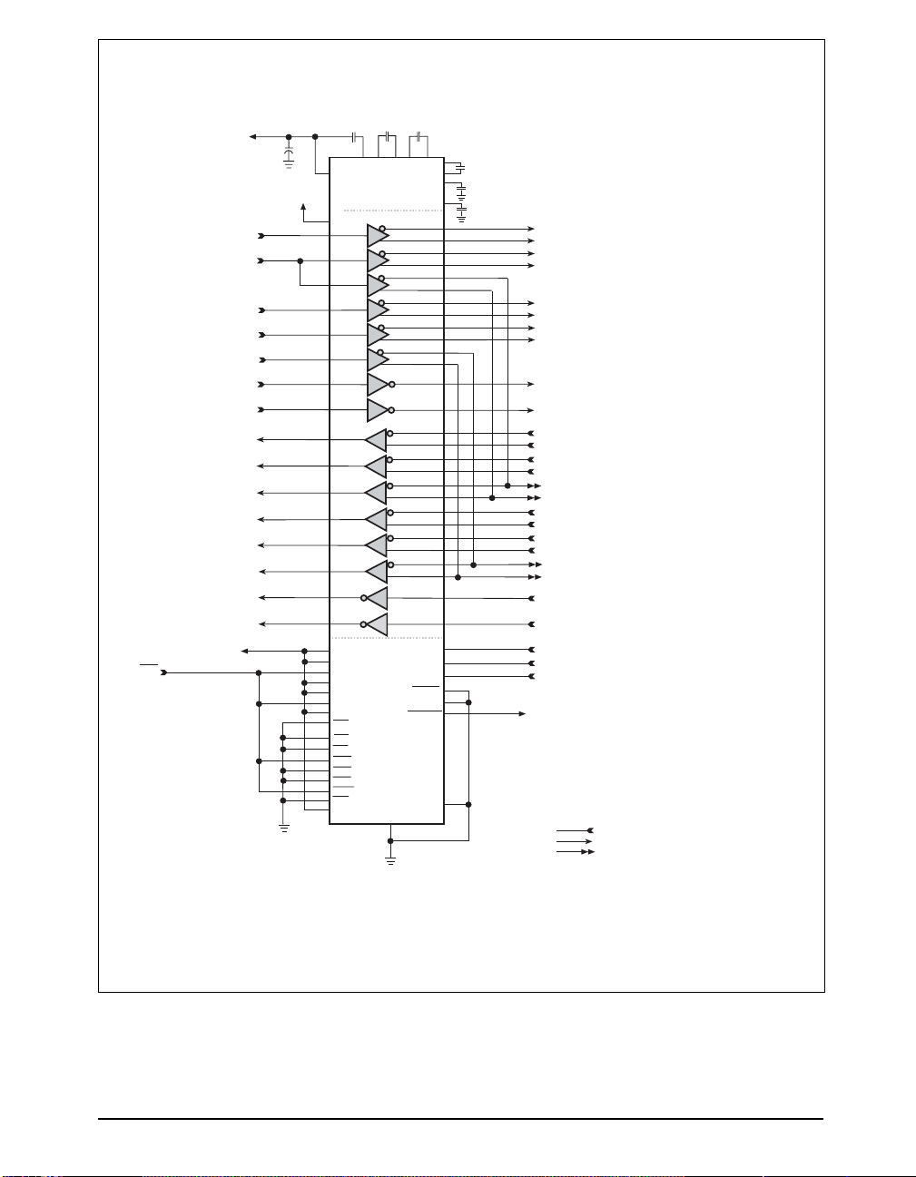
Figure 51. SP3508 Typical Operating Configuration to Serial Port Connector with DCE/DTE programmability
Date: 10/12/04 SP3508 Enhanced WAN Multi–Mode Serial Transceiver © Copyright 2004 Sipex Corporation
31
Page 32
PACKAGE: 100 PIN LQFP
PIN 1
C
L
A2
D
D1
0.2 RAD MAX.
c
0.08 RAD MIN.
11°-13°
0°MIN
E1
E
0°–7°
11°-13°
L
L1
C
L
A
A
Seating
b
e
A1
Plane
DIMENSIONS
Minimum/Maximum
(mm)
SYMBOL
A
A1
A2
b
D
D1
e
E
E1
N
100–PIN LQFP
JEDEC MS-026
(BED) Variation
MIN NOM MAX
1.60
0.05 0.15
1.35 1.40 1.45
0.17 0.22 0.27
16.00 BSC
14.00 BSC
0.50 BSC
16.00 BSC
14.00 BSC
100
COMMON DIMENSIONS
SYMBL MIN NOM MAX
c 0.09 0.20
L 0.45 0.60 0.75
L1 1.00 REF
100 PIN LQFP
Date: 10/12/04 SP3508 Enhanced WAN Multi–Mode Serial Transceiver © Copyright 2004 Sipex Corporation
32
Page 33
ORDERING INFORMATION
Part Number Temperature Range Package Types
SP3508CF .............................................0°C to +70°C ................................................. 100–pin JEDEC LQFP
SP3508EF ......................................... -40°C to +85°C ................................................. 100–pin JEDEC LQFP
Available in lead free packaging. To order add “-L” suffix to part number.
Example: SP3508EF = standard; SP3508EF-L = lead free
REVISION HISTORY
DATE REVISION DESCRIPTION
1/12/04 A Implemented tracking revision.
2/27/04 B Included Diamond column in spec table indicating which specs apply
over full operating temp. range. In figure 51, fixed typo on pin 61 and
62 from an input line to a bidirectional bus.
3/31/04 C Corrected max dimension for symbol c on LQFP package.
6/3/04 D Added tables to page 27 and 28.
10/12/04 E Certified conformance to NET1/NET2 and TBR-1 TBR-2 BY TUV
Rheinland (Test Report # TBR2/30451940.001/04)
Corporation
ANALOG EXCELLENCE
Sipex Corporation
Headquarters and
Sales Office
233 South Hillview Drive
Milpitas, CA 95035
TEL: (408) 934-7500
FAX: (408) 935-7600
Sipex Corporation reserves the right to make changes to any products described herein. Sipex does not assume any liability arising out of the
application or use of any product or circuit described herein; neither does it convey any license under its patent rights nor the rights of others.
Date: 10/12/04 SP3508 Enhanced WAN Multi–Mode Serial Transceiver © Copyright 2004 Sipex Corporation
33
 Loading...