

Page 1
®
SP3243
3 Driver/5 Receiver Intelligent +3.0V to +5.5V
RS-232 Transceivers
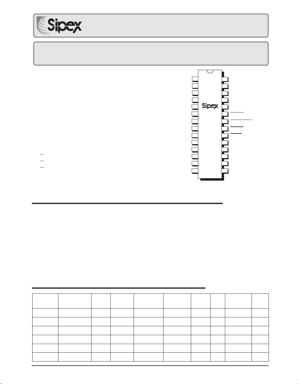
FEATURES
■ Meets true EIA/TIA-232-F Standards
from a +3.0V to +5.5V power supply
■ Interoperable with EIA/TIA-232 and
adheres to EIA/TIA-562 down to a +2.7V
power source
■
AUTO ON-LINE
®
circuitry automatically
wakes up from a 1µA shutdown
■ Regulated Charge Pump Yields Stable
RS-232 Outputs Regardless of V
Variations
CC
■ Enhanced ESD Specifications:
+15kV Human Body Model
+15kV IEC1000-4-2 Air Discharge
+8kV IEC1000-4-2 Contact Discharge
■ 250 Kbps min. transmission rate (EB)
■ 1000 Kbps min. transmission rate (EU)
■ Ideal for High Speed RS-232 Applications
1
C2+
2
C2-
3
V-
4
R
IN
1
5
IN
R
2
R
3
R4IN
R
5
T
OUT
1
T
OUT
2
OUT
T
3
T
3
T2IN
T
1
SP3243
IN
6
7
8
IN
9
10
11
12
IN
13
IN
14
Now Available in Lead Free Packaging
28
C1+
V+
27
V
26
25
GND
24
C1-
23
ONLINE
22
SHUTDOWN
21
STATUS
R
20
R
19
18
R
17
R
16
R
15
R
CC
2
1
2
3
4
5
OUT
OUT
OUT
OUT
OUT
OUT
DESCRIPTION
The SP3243 products are 3 driver/5 receiver RS-232 transceiver solutions intended for portable or handheld applications such as notebook and palmtop computers. The SP3243 includes one complementary
receiver that remains alert to monitor an external device's Ring Indicate signal while the device is
shutdown. The SP3243E and EB devices feature slew-rate limited outputs for reduced crosstalk and
EMI. The "U" and "H" series are optimized for high speed with data rates up to 1Mbps, easily meeting
the demands of high speed RS-232 applications. The SP3243 series uses an internal high-efficiency,
charge-pump power supply that requires only 0.1µF capacitors in 3.3V operation. This charge pump and
Sipex's driver architecture allow the SP3243 series to deliver compliant RS-232 performance from a single
power supply ranging from +3.0V to +5.5V. The AUTO ON-LINE
®
feature allows the device to
automatically "wake-up" during a shutdown state when an RS-232 cable is connected and a connected
peripheral is turned on. Otherwise, the device automatically shuts itself down drawing less than 1µA.
SELECTION TABLE
-3LTT
eciveDrewoP
seilppuS
3423PSV5.5+otV0.3+35sroticapac4SEYSEY82021Vk2
E3423PSV5.5+otV0.3+35sroticapac4SEYSEY82021Vk51
B3423PSV5.5+otV0.3+35sroticapac4SEYSEY82052Vk2
BE3423PSV5.5+otV0.3+35sroticapac4SEYSEY82052Vk51
U3423PSV5.5+otV0.3+35sroticapac4SEYSEY820001Vk2
UE3423PSV5.5+otV0.3+35sroticapac4SEYSEY820001Vk51
Date: 1/11/05 SP3243 +3.0V to +5.5V RS-232 Transceivers © Copyright 2005 Sipex Corporation
232-SR
srevirD
232-SR
srevieceR
lanretxE
stnenopmoC
®
ENIL-NOOTUA
yrtiucriC
fo#
etatS
sniP
deetnaruaG
DSE
etaRataD
1
gnitaR
Page 2
ABSOLUTE MAXIMUM RATINGS
These are stress ratings only and functional operation
of the device at these ratings or any other above those
indicated in the operation sections of the specifications
below is not implied. Exposure to absolute maximum
Power Dissipation per package
28-pin SOIC (derate 12.7mW/oC above +70oC)....1000mW
28-pin SSOP (derate 11.2mW/oC above +70oC).....900mW
28-pin TSSOP (derate 13.2mW/oC above +70oC)......1059mW
32-pin MLPQ (derate 29.4mW/oC above +70oC)........2352mW
rating conditions for extended periods of time may
affect reliability and cause permanent damage to the
device.
VCC.......................................................-0.3V to +6.0V
NOTE 1: V+ and V- can have maximum magnitudes of
7V, but their absolute difference cannot exceed 13V.
V+ (NOTE 1).......................................-0.3V to +7.0V
V- (NOTE 1)........................................+0.3V to -7.0V
V+ + |V-| (NOTE 1)...........................................+13V
ICC (DC VCC or GND current).........................+100mA
Input Voltages
TxIN, ONLINE,
SHUTDOWN, ....................................-0.3V to +6.0V
RxIN...................................................................+15V
Output Voltages
TxOUT.............................................................+13.2V
RxOUT, STATUS.......................-0.3V to (VCC +0.3V)
Short-Circuit Duration
TxOUT....................................................Continuous
Storage Temperature......................-65°C to +150°C
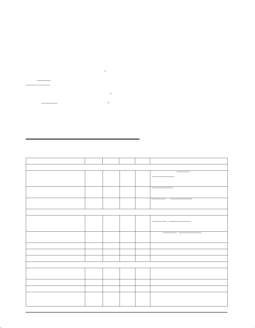
ELECTRICAL CHARACTERISTICS
Unless otherwise noted, the following specifications apply for VCC = +3.0V to +5.5V with T
C1 - C4 = 0.1µF. Typical values apply at VCC = +3.3V or +5.0V and T
= 25°C.
AMB
AMB
= T
MIN
to T
MAX
,
PARAMETER MIN. TYP. MAX. UNITS CONDITIONS
DC CHARACTERISTICS
Supply Current,AUTO ON-LINE
®
1.0 10 µA All RxIN open, ONLINE = GND,
SHUTDOWN = VCC, VCC = +3.3V,
T
= +25°C, TxIN = GND or V
AMB
Supply Current, Shutdown 1.0 10 µA SHUTDOWN = GND, V
T
= +25°C, TxIN = VCC or GND
AMB
= +3.3V,
CC
CC
Supply Current, 0.3 1.0 mA ONLINE = SHUTDOWN = VCC, no load,
AUTO ON-LINE® Disabled
VCC = +3.3V, T
= +25°C, TxIN = GND or V
AMB
LOGIC INPUTS AND RECEIVER OUTPUTS
Input Logic Threshold VCC = +3.3V or +5.0V, TxIN,
LOW 0.8 V ONLINE, SHUTDOWN
HIGH 2.4 V
Input Leakage Current ±0.01 ±1.0 µA TxIN, ONLINE, SHUTDOWN,
T
= +25°C, VIN = 0V to V
AMB
Output Leakage Current ±0.05 ±10 µA Receivers disabled, V
Output Voltage LOW 0.4 V I
Output Voltage HIGH VCC - 0.6 VCC - 0.1 V I
= 1.6mA
OUT
= -1.0mA
OUT
= 0V to V
OUT
CC
CC
DRIVER OUTPUTS
Output Voltage Swing ±5.0 ±5.4 V All driver outputs loaded with 3KΩ to GND,
T
= +25°C
AMB
Output Resistance 300 Ω VCC = V+ = V- = 0V, V
Output Short-Circuit Current ±35 ±60 mA V
OUT
= 0V
Output Leakage Current ±25 µAVCC = 0V or 3.0V to 5.5V, V
OUT
= ±2V
OUT
= ±12V,
Drivers disabled
CC
Date: 1/11/05 SP3243 +3.0V to +5.5V RS-232 Transceivers © Copyright 2005 Sipex Corporation
2
Page 3
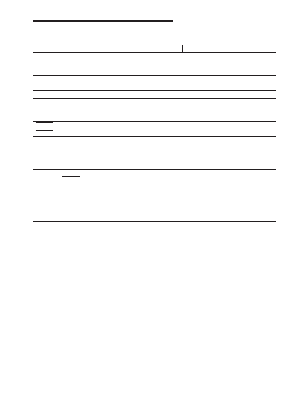
ELECTRICAL CHARACTERISTICS
Unless otherwise noted, the following specifications apply for VCC = +3.0V to +5.5V with T
C1 - C4 = 0.1µF. Typical values apply at VCC = +3.3V or +5.0V and T
= 25°C.
AMB
AMB
= T
MIN
to T
MAX
,
PARAMETER MIN. TYP. MAX. UNITS CONDITIONS
RECEIVER INPUTS
Input Voltage Range -15 15 V
Input Threshold LOW 0.6 1.2 V V
Input Threshold LOW 0.8 1.5 V V
CC
CC
= 3.3V
= 5.0V
Input Threshold HIGH 1.5 2.4 V VCC = 3.3V
Input Threshold HIGH 1.8 2.4 V VCC = 5.0V
Input Hysteresis 0.3 V
Input Resistance 3 5 7 kΩ
AUTO ON-LINE® CIRCUITRY CHARACTERISTICS (ONLINE = GND, SHUTDOWN = VCC) 25°C
STATUS Output Voltage LOW 0.4 V I
STATUS Output Voltage HIGH VCC - 0.6 V I
= 1.6mA
OUT
= -1.0mA
OUT
Receiver Threshold to Drivers 350 µS Figure 20
Enabled (t
ONLINE
)
Receiver Positive or Negative 0.2 µS Figure 20
Threshold to STATUS HIGH
(t
)
STSH
Receiver Positive or Negative 30 µS Figure 20
Threshold to STATUS LOW
(t
)
STSL
TIMING CHARACTERISTICS
Maximum Data Rate (U) 1000 Kbps RL = 3KΩ, CL = 250pF, one driver active
(H) 460 RL = 3KΩ, CL = 1000pF, one driver active
(B) 250 RL = 3KΩ, CL = 1000pF, one driver active.
( - ) 120 RL = 3KΩ, CL = 1000pF, one driver active
Receiver Propagation Delay
t
t
PHL
PLH
0.15 µs Receiver input to Receiver output, CL = 150pF
0.15
Receiver Output Enable Time 200 ns Normal operation
Receiver Output Disable Time 200 ns Normal operation
Driver Skew (E, EB) 100 500 ns | t
PHL
- t
PLH
|
(EU) 50 100
Receiver Skew 50 ns | t
Transition-Region Slew Rate (U) 90 V/µsV
- t
|
PHL
PLH
= 3.3V, RL = 3KΩ, T
CC
AMB
= 25°C,
(EB) 6 30 measurements taken from -3.0V to +3.0V or
+3.0V to -3.0V
Date: 1/11/05 SP3243 +3.0V to +5.5V RS-232 Transceivers © Copyright 2005 Sipex Corporation
3
Page 4
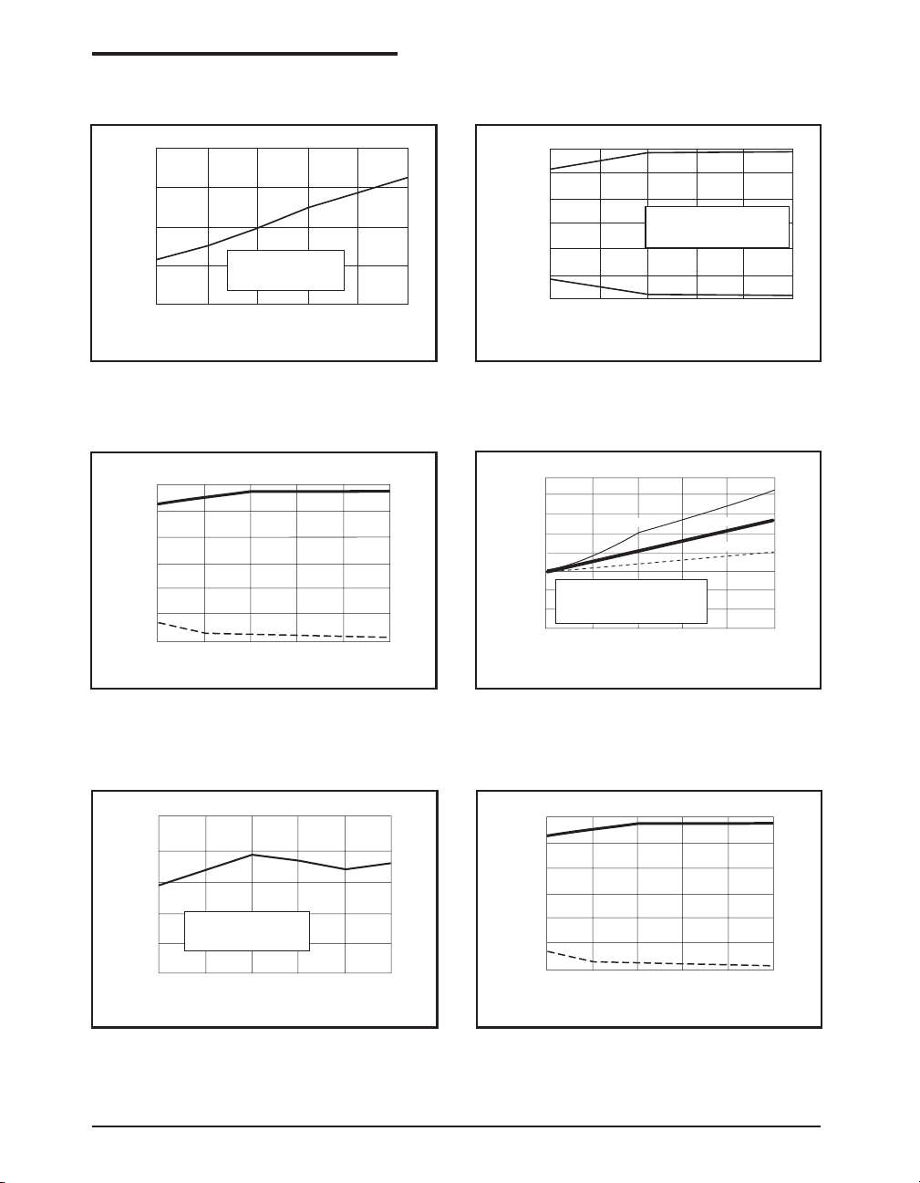
TYPICAL PERFORMANCE CHARACTERISTICS
Unless otherwise noted, the following performance characteristics apply for VCC = +3.3V, 1000kbps data rate, all drivers
loaded with 3kΩ, 0.1µF charge pump capacitors, and T
= +25°C.
AMB
200
150
100
Skew (ns)
50
0
0 250 500 1000 1500 2000
T1 at 500Kbps
T2 at 31.2Kbps
All TX loaded 3K // CLoad
Load Capacitance (pF)
Figure 1. Transmitter Skew VS. Load Capacitance
6
4
2
0
-2
Voltage (V)
Transmitter Output
-4
-6
2.7 3 3.5 4 4.5 5
TxOUT +
TxOUT -
Supply Voltage (V
)
DC
Figure 3. Transmitter Output Voltage VS. Load
Capacitance for the SP3243EU
6
4
2
0
Voltage (V)
-2
Transmitter Output
-4
-6
2.7 3 3.5 4 4.5 5
1Driver at 1Mbps
Other Drivers at 62.5Kbps
All Drivers Loaded with 3K // 250pF
Supply Voltage (V)
Figure 2. Transmitter Output Voltage VS. Supply
Voltage for the SP3243EU
40
35
30
(mA)
25
20
15
10
Supply Current
5
0
0 1000 2000 3000 4000 5000
250Kbps
1 Transmitter at full Data Rate
2 Transmitters at 15.5 Kbps
All Transmitters loades 3K + Load Cap
Load Capacitance (pF)
120Kbps
20Kbps
Figure 4. Supply Current VS. Load Capacitance for the
SP3243EU
25
20
15
10
1 Transmitter at 250Kbps
2 Transmitters at 15.6Kbps
5
Supply Current (mA)
Figure 5. Supply Current VS. Supply Voltage for the
SP3243EU
Date: 1/11/05 SP3243 +3.0V to +5.5V RS-232 Transceivers © Copyright 2005 Sipex Corporation
All drivers loaded with 3K // 1000pF
0
2.7 3 3.5 4 4.5 5
Supply Voltage (V
)
DC
Figure 6. Transmitter Output Voltage VS. Supply
Voltage for the SP3243EU
6
4
2
0
-2
Voltage (V)
Transmitter Output
-4
-6
2.7 3 3.5 4 4.5 5
TxOUT +
TxOUT -
Supply Voltage (V
)
DC
4
Page 5
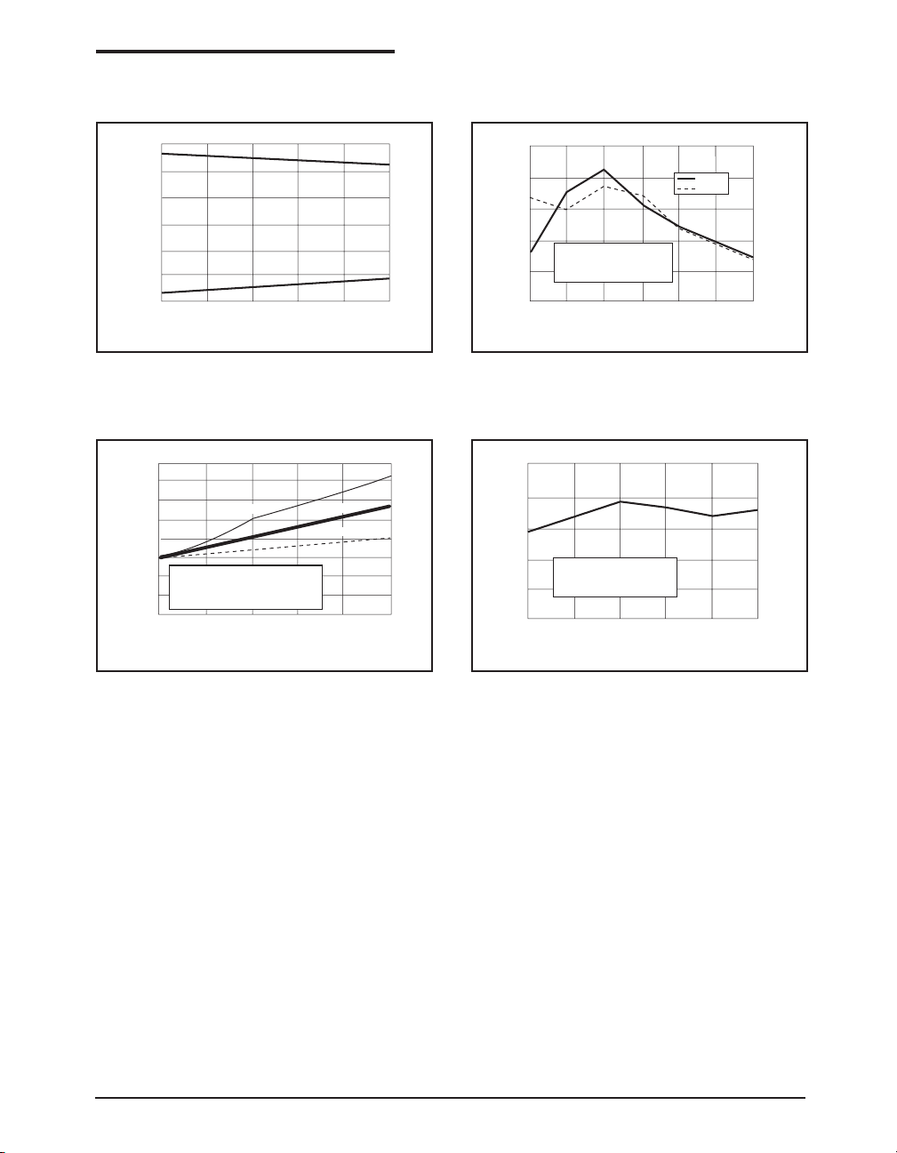
TYPICAL PERFORMANCE CHARACTERISTICS
Unless otherwise noted, the following performance characteristics apply for VCC = +3.3V, 1000kbps data rate, all drivers
loaded with 3kΩ, 0.1µF charge pump capacitors, and T
= +25°C.
AMB
6
4
TxOUT +
2
0
-2
Voltage (V)
-4
Transmitter Output
-6
TxOUT -
0 1000 2000 3000 4000 5000
Load Capacitance (pF)
Figure 7. Transmitter Output Voltage VS. Load
Capacitance
40
35
30
(mA)
25
250Kbps
20
15
1 Transmitter at full Data Rate
10
2 Transmitters at 15.5 Kbps
Supply Current
5
All Transmitters loades 3K + Load Cap
0
0 1000 2000 3000 4000 5000
Load Capacitance (pF)
120Kbps
20Kbps
25
20
- Slew
+ Slew
15
10
Slew rate (V/µs)
1 Transmitter at 250Kbps
2 Transmitter at 15.6Kbps
5
All drivers loaded 3K + Load Cap
0
0 500 1000 2000 3000 4000 5000
Load Capacitance (pF)
Figure 8. Slew Rate VS. Load Capacitance
25
20
15
10
1 Transmitter at 250Kbps
2 Transmitters at 15.6Kbps
5
Supply Current (mA)
All drivers loaded with 3K // 1000pF
0
2.7 3 3.5 4 4.5 5
Supply Voltage (V
)
DC
Figure 9. Supply Current VS. Load Capacitance
Date: 1/11/05 SP3243 +3.0V to +5.5V RS-232 Transceivers © Copyright 2005 Sipex Corporation
Figure 10. Supply Current VS. Supply Voltage
5
Page 6
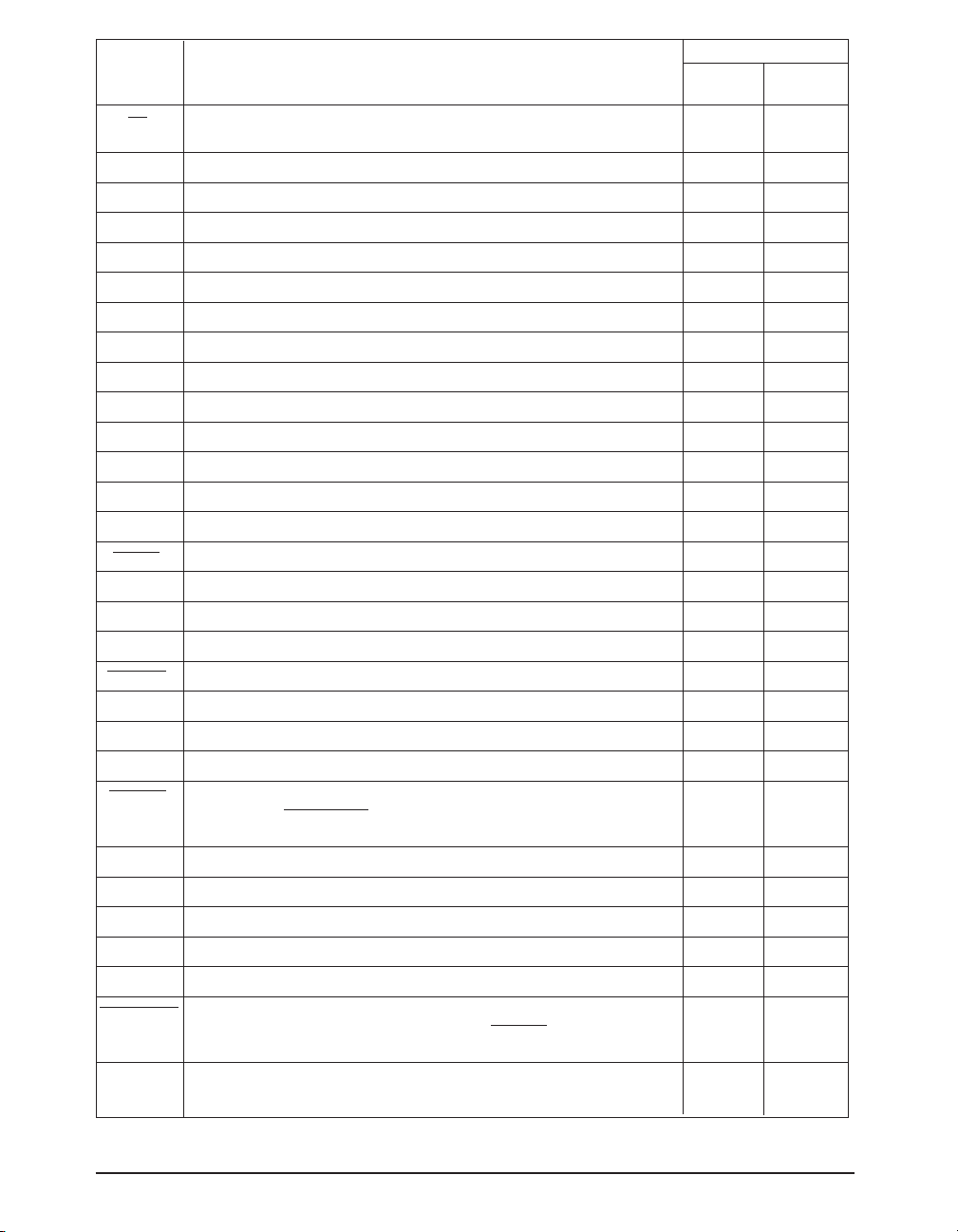
PIN NUMBER
NAME FUNCTION SP3243EU MLPQ
SP3243EUCR
EN Receiver Enable. Apply logic LOW for normal operation. - -
Apply logic HIGH to disable the receiver outputs (high-Z state).
C1+ Positive terminal of the voltage doubler charge-pump capacitor. 28 28
V+ Regulated +5.5V output generated by the charge pump. 27 26
C1- Negative terminal of the voltage doubler charge-pump capacitor. 24 22
C2+ Positive terminal of the inverting charge-pump capacitor. 1 29
C2- Negative terminal of the inverting charge-pump capacitor. 2 31
V- Regulated -5.5V output generated by the charge pump. 3 32
R1IN RS-232 receiver input. 4 2
R2IN RS-232 receiver input. 5 3
R3IN RS-232 receiver input. 6 4
R4IN RS-232 receiver input. 7 5
R5IN RS-232 receiver input. 8 6
R1OUT TTL/CMOS receiver output. 19 17
R2OUT TTL/CMOS receiver output. 18 16
R2OUT Non-inverting receiver-2 output, active in shutdown. 20 18
R3OUT TTL/CMOS receiver output. 17 15
R4OUT TTL/CMOS receiver output. 16 14
R5OUT TTL/CMOS receiver output. 15 13
STATUS TTL/CMOS Output indicating online and shutdown status. 21 19
T1IN TTL/CMOS driver input. 14 12
T2IN TTL/CMOS driver input. 13 11
T3IN TTL/CMOS driver input. 12 10
ONLINE Apply logic HIGH to override Auto-Online circuitry keeping 23 21
drivers active (SHUTDOWN must also be logic HIGH,
refer to Table 2).
T1OUT RS-232 driver output. 9 7
T2OUT RS-232 driver output. 10 8
T3OUT RS-232 driver output. 11 9
GND Ground. 25 23
V
+3.0V to +5.5V supply voltage. 26 25
CC
SHUTDOWN Apply logic LOW to shut down drivers and charge pump. 22 20
This overrides all AUTO ON-LINE® circuitry and ONLINE
(refer to Table 2).
NC No Connection - 1,24,27,30
Table 1. Device Pin Description
Date: 1/11/05 SP3243 +3.0V to +5.5V RS-232 Transceivers © Copyright 2005 Sipex Corporation
6
Page 7
+
0.1µF
C5
+
0.1
C1
+
C2
0.1
TTL/CMOS
INPUTS
TTL/CMOS
OUTPUTS
To µP Supervisor
Circuit
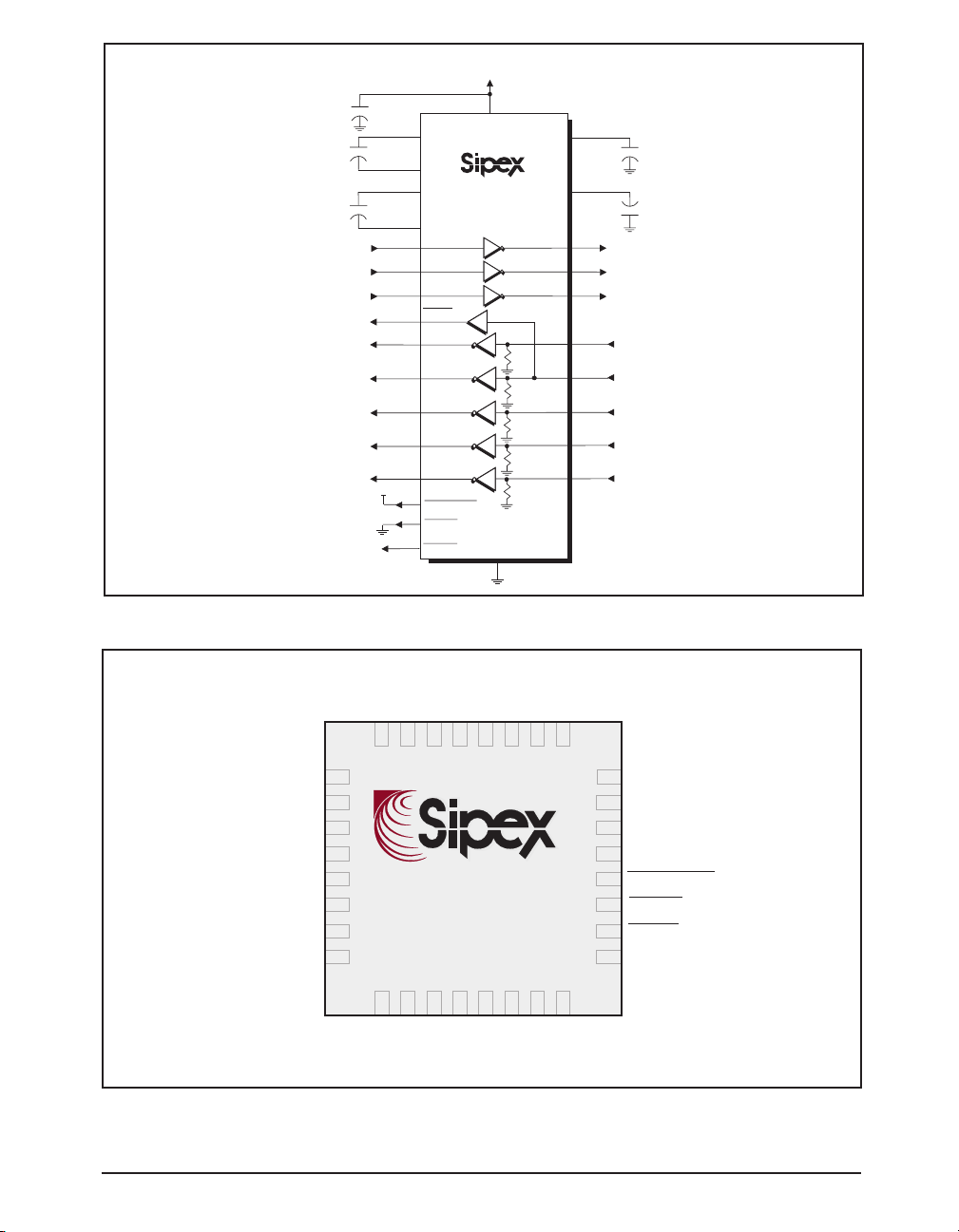
Figure 15. SP3243 Typical Operating Circuit
V
CC
26
CC
R
3
1
2
3
4
IN
OUT
OUT
OUT
OUT
OUT
5
V
SP3243
GND
25
5KΩ
5KΩ
5KΩ
5KΩ
5KΩ
27
V+
V-
T
OUT
1
T
OUT
2
T
OUT
3
R1IN
R
IN
2
IN
R
3
R
IN
4
R
IN
5
+
µ
F
0.1
C3
3
µ
F
0.1
C4
+
9
10
RS-232
OUTPUTS
11
4
5
6
RS-232
INPUTS
7
8
28
C1+
µ
F
24
C1-
1
C2+
µ
F
2
C2-
T1IN
14
T2IN
13
T
12
R2OUT
20
R
19
R
18
R
17
R
16
15
V
CC
22
SHUTDOWN
23
ONLINE
21
STATUS
V
272625
®
®
OUT
OUT
4
3
R
R
CC
OUT
2
R
24
NC
23
GND
22
C1-
21
ONLINE
20
SHUTDOWN
19
STATUS
18
R2OUT
17
R
OUT
1
T
T
R
R
R3IN
R4IN
R5IN
OUT
1
OUT
2
NC
1
2
IN
IN
1
2
3
4
5
6
7
8
V-
C2-NCC2+
C1+NCV+
3231302928
SP3243
9
10111213141516
IN
IN
IN
3
2
1
OUT
3
T
T
OUT
T
T
5
R
Figure 13. SP3243 QFN Pinout Configuration
Date: 1/11/05 SP3243 +3.0V to +5.5V RS-232 Transceivers © Copyright 2005 Sipex Corporation
7
Page 8
DESCRIPTION
The SP3243 transceivers meet the EIA/TIA-232
and ITU-T V.28/V.24 communication protocols
and can be implemented in battery-powered,
portable, or hand-held applications such as notebook or palmtop computers. The SP3243 devices feature Sipex's proprietary and patented
(U.S.-- 5,306,954) on-board charge pump circuitry that generates ±5.5V RS-232 voltage levels from a single +3.0V to +5.5V power supply.
The SP3243EU devices can operate at a data rate
of 1000kbps fully loaded.
The SP3243 is a 3-driver/5-receiver device, ideal
for portable or hand-held applications. The
SP3243 includes one complementary
always-active receiver that can monitor an
external device (such as a modem) in shutdown.
This aids in protecting the UART or serial
controller IC by preventing forward biasing
of the protection diodes where VCC may be
disconnected.
The SP3243 series is an ideal choice for power
sensitive designs. The SP3243 devices feature
V
CC
RESET
UART
or
Serial µC
µP
Supervisor
IC
+
0.1µF
C5
+
0.1µF
C1
+
C2
0.1µF
TxD
RTS
DTR
RxD
CTS
DSR
DCD
RI
V
CC
V
IN
28
C1+
24
C1-
1
C2+
2
C2-
T1IN
14
T2IN
13
T
12
R2OUT
20
R
19
R
18
R
17
R
16
15
22
SHUTDOWN
23
ONLINE
21
STATUS
26
V
CC
27
V+
+
0.1µF
C3
SP3243
IN
3
OUT
1
OUT
2
OUT
3
OUT
4
R
OUT
5
GND
3
V-
0.1µF
C4
+
OUT
T
9
1
OUT
T
10
2
RS-232
OUTPUTS
T
OUT
11
3
R1IN
4
5KΩ
R
IN
5
2
5KΩ
IN
R
6
3
RS-232
5KΩ
5KΩ
5KΩ
25
INPUTS
R
IN
4
7
R
IN
5
8
®
AUTO ON-LINE
circuitry which reduces the
power supply drain to a 1µA supply current. In
many portable or hand-held applications, an RS232 cable can be disconnected or a connected
peripheral can be turned off. Under these conditions, the internal charge pump and the drivers
will be shut down. Otherwise, the system automatically comes online. This feature allows design engineers to address power saving concerns
without major design changes.
THEORY OF OPERATION
The SP3243 series is made up of four basic
circuit blocks:
1. Drivers
2. Receivers
3. the Sipex proprietary charge pump, and
4. AUTO ON-LINE
®
circuitry.
Drivers
The drivers are inverting level transmitters that
convert TTL or CMOS logic levels to 5.0V EIA/
TIA-232 levels with an inverted sense relative to
the input logic levels. Typically, the RS-232
output voltage swing is +5.4V with no load and
+5V minimum fully loaded. The driver outputs
are protected against infinite short-circuits to
ground without degradation in reliability. These
drivers comply with the EIA-TIA-232-F and all
previous RS-232 versions. Unused drivers inputs should be connected to GND or VCC.
The drivers have a minimum data rate of 250kbps
(EB) or 1000kbps (EU) fully loaded.
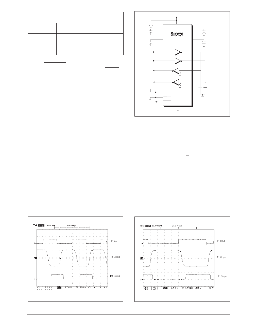
Figure 17 shows a loopback test circuit used to
test the RS-232 Drivers. Figure 18 shows the test
results where one driver was active at 1Mbps and
all three drivers loaded with an RS-232 receiver
in parallel with a 250pF capacitor. Figure 19
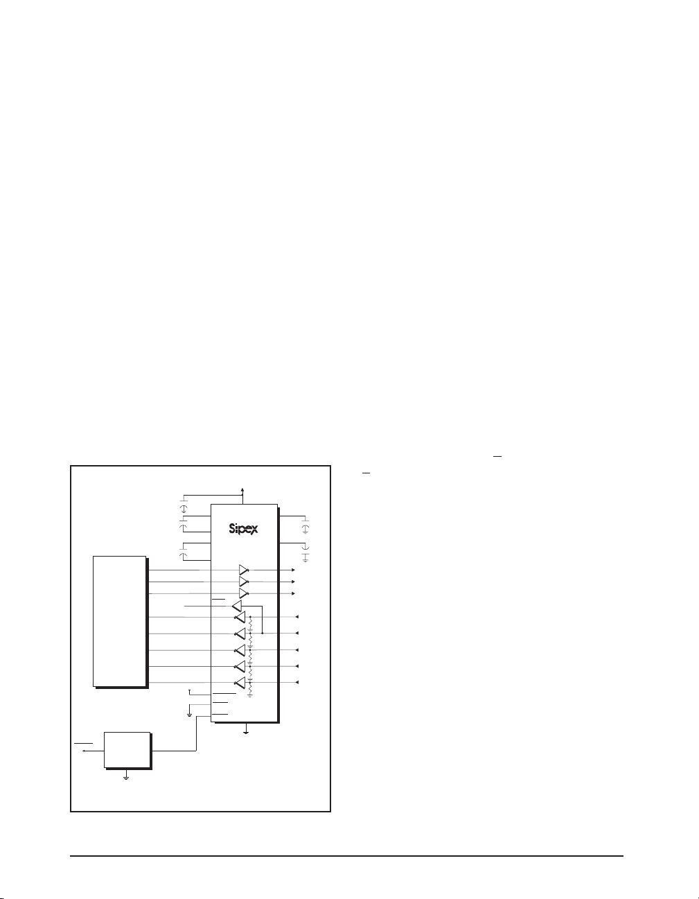
Figure 16. Interface Circuitry Controlled by Microprocessor Supervisory Circuit
Date: 1/11/05 SP3243 +3.0V to +5.5V RS-232 Transceivers © Copyright 2005 Sipex Corporation
8
Page 9
UE3423PS:ECIVED
NWODTUHST
TUORXTUOR2TUO
X
0ZhgiHZhgiHevitcA
1evitcAevitcAevitcA
Table 2. SHUTDOWN Truth Tables
Note: In AUTO ON-LINE® Mode where ONLINE =
GND and SHUTDOWN = VCC, the device will shut down
if there is no activity present at the Receiver inputs.
+3V to +5V
+
0.1µF
C5
C1
C2
TTL/CMOS
INPUTS
TTL/CMOS
OUTPUTS
V
CC
To µP Supervisor
Circuit
+
+
0.1µF
0.1µF
C1+
C1-
SP3243
C2+
C2-
IN
T
1
T
IN
X
OUT
R
1
R
OUT
X
SHUTDOWN
ONLINE
STATUS
CC
V
GND
V+
OUT
T
1
OUT
T
X
IN
R
1
5kΩ
R
IN
X
5kΩ
+
0.1µF
C3
V-
1000pF
0.1µF
C4
+
1000pF
Figure 17. Loopback Test Circuit for RS-232 Driver
Data Transmission Rates
shows the test results of the loopback circuit with
all drivers active at 250kbps with typical
RS-232 loads in parallel with 1000pF capacitors. A
superior RS-232 data transmission rate of 1Mbps
makes the SP3243EU an ideal match for high
speed LAN and personal computer peripheral
applications.
Receivers
The receivers convert +5.0V EIA/TIA-232
levels to TTL or CMOS logic output levels.
Receivers are active when the AUTO ON-LINE
circuitry is enabled or when in shutdown.
During the shutdown, the receivers will continue
to be active. If there is no activity present at the
receivers for a period longer than 100µs or when
SHUTDOWN is enabled, the device goes into a
standby mode where the circuit draws 1µA. The
®
Figure 18. Loopback Test results at 1Mbps
Figure 19. Loopback Test results at 250Kbps
Date: 1/11/05 SP3243 +3.0V to +5.5V RS-232 Transceivers © Copyright 2005 Sipex Corporation
9
Page 10

truth table logic of the SP3243 driver and receiver
outputs can be found in Table 2.
The SP3243 includes an additional non-inverting receiver with an output R
OUT. R2OUT is an
2
extra output that remains active and
monitors activity while the other receiver
outputs are forced into high impedance.
This allows Ring Indicator (RI) from a
peripheral to be monitored without forward
biasing the TTL/CMOS inputs of the other
devices connected to the receiver outputs.
Since receiver input is usually from a transmission line where long cable lengths and system
interference can degrade the signal, the inputs
have a typical hysteresis margin of 300mV. This
ensures that the receiver is virtually immune to
noisy transmission lines. Should an input be left
unconnected, an internal 5KΩ pulldown resistor
to ground will commit the output of the receiver
to a HIGH state.
Charge Pump
The charge pump is a Sipex–patented design
(U.S. 5,306,954) and uses a unique approach
compared to older less–efficient designs. The
charge pump still requires four external
capacitors, but uses a four–phase voltage
shifting technique to attain symmetrical 5.5V
power supplies. The internal power supply consists of a regulated dual charge pump that provides output voltages 5.5V regardless of the
input voltage (V
range. This is important to maintain compliant
) over the +3.0V to +5.5V
CC
RS-232 levels regardless of power supply
fluctuations.
The charge pump operates in a discontinuous
mode using an internal oscillator. If the output
voltages are less than a magnitude of 5.5V, the
charge pump is enabled. If the output voltages
exceed a magnitude of 5.5V, the charge pump is
disabled. This oscillator controls the four phases
of the voltage shifting. A description of each
phase follows.
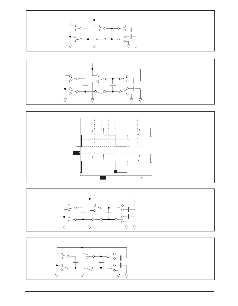
Phase 1
— VSS charge storage — During this phase of
the clock cycle, the positive side of capacitors
C1 and C2 are initially charged to VCC. C
then switched to GND and the charge in C
transferred to C
VCC, the voltage potential across capacitor C2 is
–
. Since C
2
+
is connected to
2
+
is
l
–
is
1
now 2 times VCC.
Phase 2
— VSS transfer — Phase two of the clock
connects the negative terminal of C2 to the V
storage capacitor and the positive terminal of C
SS
to GND. This transfers a negative generated
voltage to C3. This generated voltage is
regulated to a minimum voltage of -5.5V.
Simultaneous with the transfer of the voltage to
C3, the positive side of capacitor C1 is switched
to VCC and the negative side is connected to
GND.
Phase 3
— VDD charge storage — The third phase of the
clock is identical to the first phase — the charge
transferred in C1 produces –VCC in the negative
terminal of C1, which is applied to the negative
side of capacitor C2. Since C
voltage potential across C2 is 2 times VCC.
+
is at VCC, the
2
Phase 4
— VDD transfer — The fourth phase of the clock
connects the negative terminal of C2 to GND,
and transfers this positive generated voltage
across C2 to C4, the VDD storage capacitor. This
voltage is regulated to +5.5V. At this voltage,
the internal oscillator is disabled. Simultaneous
with the transfer of the voltage to C4, the
positive side of capacitor C1 is switched to V
and the negative side is connected to GND,
CC
allowing the charge pump cycle to begin again.
The charge pump cycle will continue as long as
the operational conditions for the internal
oscillator are present.
Since both V+ and V– are separately generated
from VCC, in a no–load condition V+ and V– will
be symmetrical. Older charge pump approaches
that generate V– from V+ will show a decrease in
the magnitude of V– compared to V+ due to the
inherent inefficiencies in the design. The clock
rate for the charge pump typically operates at
greater than 250kHz. The external capacitors
can be as low as 0.1µF with a 16V breakdown
voltage rating.
2
Date: 1/11/05 SP3243 +3.0V to +5.5V RS-232 Transceivers © Copyright 2005 Sipex Corporation
10
Page 11
eulavroticapacpmupegrahcdednemmocermuminiM
VegatloVtupnI
CC
V6.3otV0.3
V5.5otV5.4Fu33.0=4C-2C,Fu740.0=1C
V5.5otV0.3Fu22.0=4C–1C
The Sipex-patented charge pumps are designed
to operate reliably with a range of low cost
capacitors. Either polarized or non polarized
capacitors may be used. If polarized capacitors
are used they should be oriented as shown in the
Typical Operating Circuit. The V+ capacitor
may be connected to either ground or Vcc
(polarity reversed.)
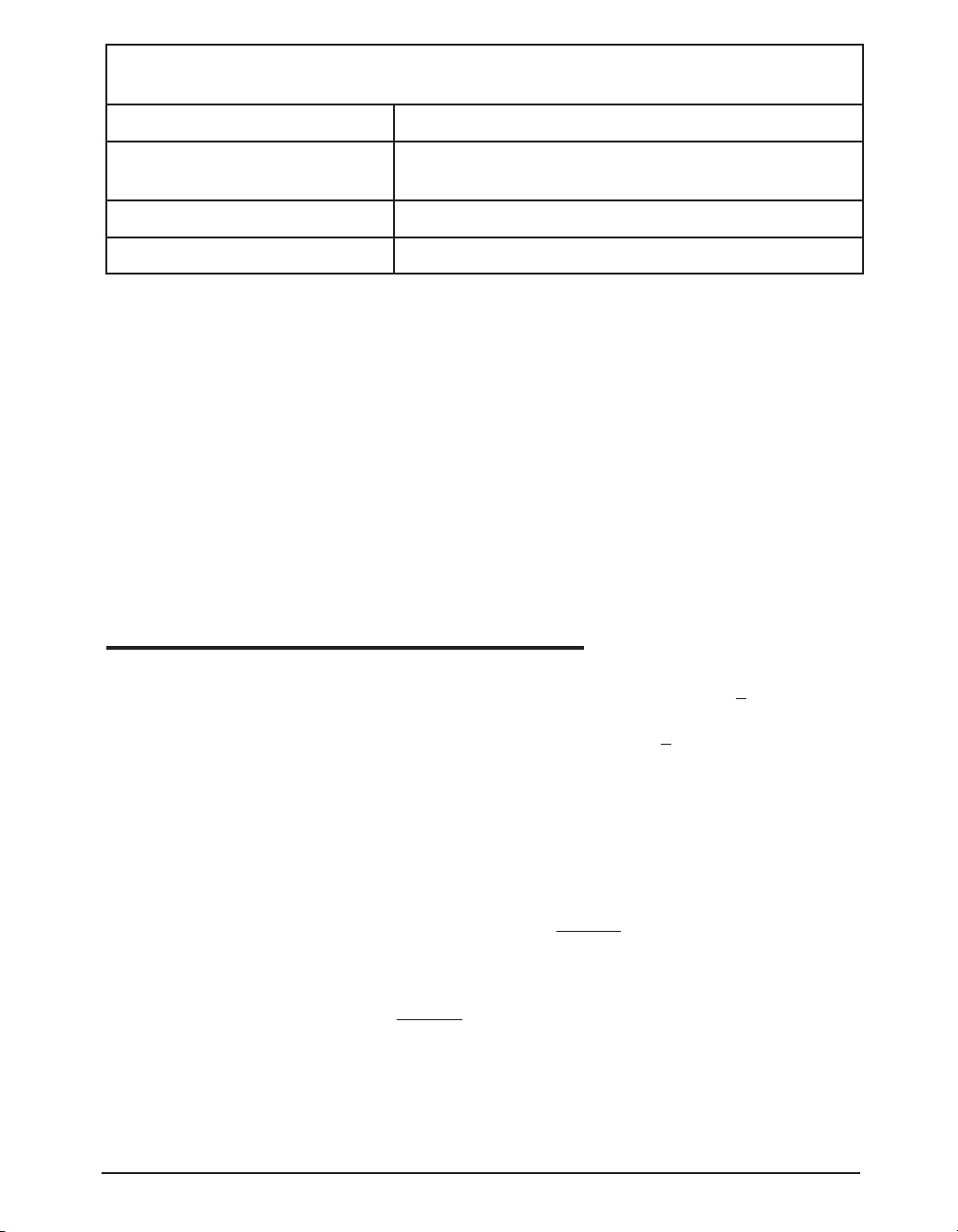
The charge pump operates with 0.1µF capacitors
for 3.3V operation. For other supply voltages,
see the table for required capacitor values. Do
not use values smaller than those listed. Increasing
the capacitor values (e.g., by doubling in value)
XX23PSrofeulavroticapacpmupegrahC
Fu1.0=4C–1C
reduces ripple on the transmitter outputs and
may slightly reduce power consumption. C2,
C3, and C4 can be increased without changing
C1’s value.
For best charge pump efficiency locate the charge
pump and bypass capacitors as close as possible
to the IC. Surface mount capacitors are best for
this purpose. Using capacitors with lower
equivalent series resistance (ESR) and selfinductance, along with minimizing parasitic PCB
trace inductance will optimize charge pump
operation. Designers are also advised to consider
that capacitor values may shift over time and
operating temperature.
AUTO ONLINE CIRCUITRY
The SP3243 devices have a patent pending AUTO
ON-LINE® circuitry on board that saves power
in applications such as laptop computers, palmtop
(PDA) computers and other portable systems.
input typically sees at least +3V, which are
generated from the transmitters at the other end
of the cable with a +5V minimum. When the
external transmitters are disabled or the cable is
disconnected, the receiver inputs will be pulled
The SP3243 devices incorporate an AUTO ON-
LINE® circuit that automatically enables itself
when the external transmitters are enabled and
the cable is connected. Conversely, the AUTO
ON-LINE® circuit also disables most of the
internal circuitry when the device is not being
down by their internal 5kΩ resistors to ground.
When this occurs over a period of time, the
internal transmitters will be disabled and the
device goes into a shutdown or standy mode.
When ONLINE is HIGH, the AUTO ON-LINE
mode is disabled.
used and goes into a standby mode where the
device typically draws 1mA. This function can
also be externally controlled by the ONLINE
pin. When this pin is tied to a logic LOW, the
The AUTO ON-LINE® circuit has two stages:
1) Inactive Detection
2) Accumulated Delay
AUTO ON-LINE® function is active. Once active, the device is enabled until there is no
activity on the receiver inputs. The receiver
Date: 1/11/05 SP3243 +3.0V to +5.5V RS-232 Transceivers © Copyright 2005 Sipex Corporation
11
®
Page 12
RECEIVER
RS-232 INPUT
VOLTAGES
STATUS
+2.7V
0V
-2.7V
V
CC
0V
t
STSL
t
STSH
t
ONLINE
S
H
U
T
D
O
W
N
DRIVER
RS-232 OUTPUT
VOLTAGES
Figure 20. AUTO ON-LINE® Timing Waveforms
+5V
0V
-5V
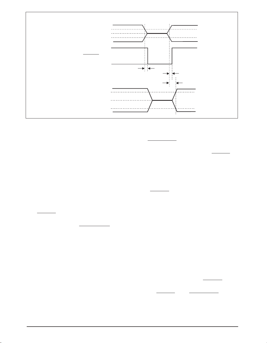
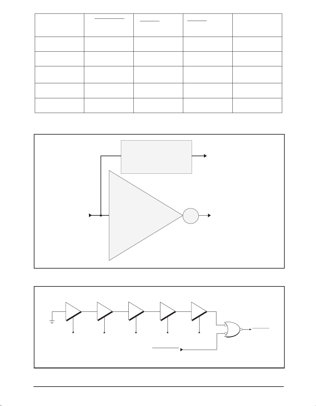
The first stage, shown in Figure 28, detects an
inactive input. A logic HIGH is asserted on
RXINACT if the cable is disconnected or the
external transmitters are disabled. Otherwise,
RXINACT will be at a logic LOW. This circuit is
duplicated for each of the other receivers.
The second stage of the AUTO ON-LINE® circuitry, shown in Figure 29, processes all the
receiver's RXINACT signals with an accumulated delay that disables the device to a 1µA
supply current.
The STATUS pin goes to a logic LOW when the
cable is disconnected, the external transmitters
are disabled, or the SHUTDOWN pin is
invoked. The typical accumulated delay is around
20µs.
When the SP3243 drivers or internal charge
pump are disabled, the supply current is reduced
to 1µA. This can commonly occur in hand-held
or portable applications where the RS-232 cable
is disconnected or the RS-232 drivers of the
connected peripheral are turned off.
The AUTO ON-LINE® mode can be disabled by
the SHUTDOWN pin. If this pin is a logic LOW,
the AUTO ON-LINE® function will not operate
regardless of the logic state of the ONLINE pin.
Table 3 summarizes the logic of the AUTO ONLINE® operating modes. The truth table logic of
the SP3243 driver and receiver outputs can be
found in Table 2.
The STATUS pin outputs a logic LOW signal
if the device is shutdown. This pin goes to a
logic HIGH when the external transmitters are
enabled and the cable is connected.
When the SP3243 devices are shut down, the
charge pumps are turned off. V+ charge pump
output decays to VCC, the V- output decays to
GND. The decay time will depend on the size of
capacitors used for the charge pump. Once in
shutdown, the time required to exit the shut
down state and have valid V+ and V- levels is
typically 200µs.
For easy programming, the STATUS can be
used to indicate DSR or a Ring Indicator signal.
Tying ONLINE and SHUTDOWN together
will bypass the AUTO ON-LINE® circuitry so
this connection acts like a shutdown input pin.
Date: 1/11/05 SP3243 +3.0V to +5.5V RS-232 Transceivers © Copyright 2005 Sipex Corporation
12
Page 13
VCC = +5V
–10V
V
SS
Storage Capacitor
V
DD
Storage Capacitor
C
1
C
2
C
3
C
4
+
+
++
–
–
––
VCC = +5V
Figure 21. Charge Pump — Phase 1
Figure 22. Charge Pump — Phase 2
a) C
2+
1
2
2
+5V
++
C
1
–5V –5V
C
2
––
T[]
T
C
4
+
–
+
–
C
3
Storage Capacitor
V
DD
Storage Capacitor
V
SS
+6V
0V
0V
b) C2-
T
Ch1 2.00V Ch2 2.00V M 1.00µs Ch1 1.96V
-6V
Figure 23. Charge Pump Waveforms
VCC = +5V
+5V
++
C
1
–5V
C
2
––
–5V
C
4
+
–
Storage Capacitor
V
DD
+
–
V
C
3
Storage Capacitor
SS
Figure 24. Charge Pump — Phase 3
VCC = +5V
+10V
++
C
Figure 25. Charge Pump — Phase 4
Date: 1/11/05 SP3243 +3.0V to +5.5V RS-232 Transceivers © Copyright 2005 Sipex Corporation
1
C
2
––
+
–
13
C
4
–
+
C
3
Storage Capacitor
V
DD
Storage Capacitor
V
SS
Page 14
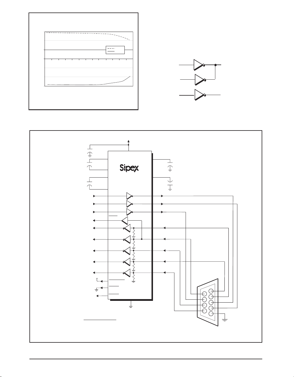
The SP3243 driver outputs are able to maintain
0
+
V
OUT
V
OUT
-
1
0
voltage under loading of up to 2.5mA per driver,
6
4
1.82
2.67
Vout+
Vout-
3.46
4.93
8.6
Transmitter Output Voltage [V]
2
0
0.62
-2
-4
-6
1.02
1.12
1.23
0.869
0.939
Load Current Per Transmitter [mA]
1.38
1.57
Figure 26. SP3243 Driver Output Voltages vs. Load
Current per Transmitter
+
0.1µF
C5
28
0.1µF
0.1µF
V
CC
C1+
24
C1-
1
C2+
2
C2-
T1IN
14
T2IN
13
T
12
3
R2OUT
20
R
19
1
R
18
2
R
3
17
R
4
16
R
15
22
SHUTDOWN
23
ONLINE
21
STATUS
IN
OUT
OUT
OUT
OUT
5
+
C1
+
C2
To µP Supervisor
Circuit
DB-9 Connector Pins:
1. Received Line Signal Detector
2. Received Data
3. Transmitted Data
4. Data Terminal Ready
5. Signal Ground (Common)
SP3243
OUT
CC
V
GND
26
25
Figure 27. Circuit for the connectivity of the SP3243 with a DB-9 connector
ensuring sufficient output for mouse-driving applications.
V
CC
27
V+
V-
T
OUT
1
OUT
T
2
T
OUT
3
R1IN
5KΩ
R
IN
2
5KΩ
IN
R
3
5KΩ
R
IN
4
5KΩ
R
IN
5
5KΩ
6. DCE Ready
7. Request to Send
8. Clear to Send
9. Ring Indicator
+
0.1µF
C3
3
0.1µF
C4
+
9
10
11
4
5
6
7
8
DB-9
Connector
6
7
8
9
1
2
3
4
5
Date: 1/11/05 SP3243 +3.0V to +5.5V RS-232 Transceivers © Copyright 2005 Sipex Corporation
14
Page 15
LANGIS232-SR
REVIECERTA
TUPNI
NWODTUHS
TUPNI
TUPNIENILNOTUPTUOSUTATS
REVIECSNART
SUTATS
SEYHGIH-HGIH
ONHGIHHGIHWOL
ONHGIHWOLWOL
SEYWOL-HGIH
ONWOL-WOL
Table 3. AUTO ON-LINE® Logic
RXIN
LOW
HIGH / LOW
HIGH / LOW
Inactive Detection Block
RS-232
Receiver Block
RXINACT
RXOUT
(Auto-Online)
nwodtuhS
(
nwodtuhS
nwodtuhS
noitarepOlamroN
noitarepOlamroN
enilnO-otuA
)
Figure 28. Stage I of AUTO ON-LINE® Circuitry
Delay
Stage
R1INACT
Delay
Stage
R2INACT
Delay
Stage
R3INACT
Delay
Stage
R4INACT
SHUTDOWN
Delay
Stage
R5INACT
STATUS
Figure 29. Stage II of AUTO ON-LINE® Circuitry
Date: 1/11/05 SP3243 +3.0V to +5.5V RS-232 Transceivers © Copyright 2005 Sipex Corporation
15
Page 16
ESD TOLERANCE
R
C
C
S
R
S
SW1
SW2
The SP3243 series incorporates ruggedized ESD
cells on all driver output and receiver input pins.
The ESD structure is improved over our previous family for more rugged applications and
environments sensitive to electro-static discharges and associated transients. The improved
ESD tolerance is at least +15kV without damage
nor latch-up.
There are different methods of ESD testing
applied:
a) MIL-STD-883, Method 3015.7
b) IEC1000-4-2 Air-Discharge
c) IEC1000-4-2 Direct Contact
The Human Body Model has been the generally
accepted ESD testing method for semiconductors. This method is also specified in
MIL-STD-883, Method 3015.7 for ESD testing.
The premise of this ESD test is to simulate the
human body’s potential to store electro-static
energy and discharge it to an integrated circuit.
The simulation is performed by using a test
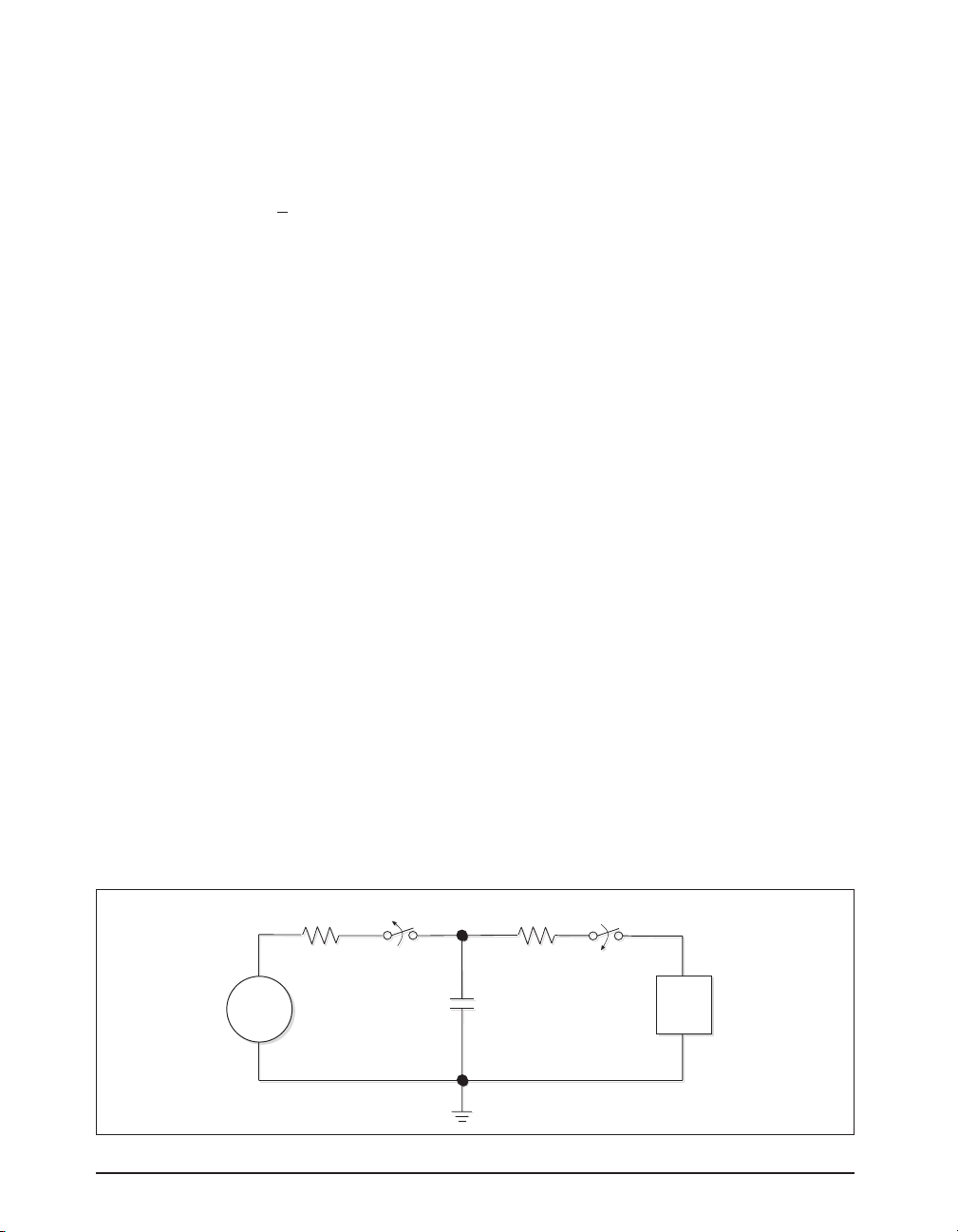
model as shown in Figure 30. This method will
test the IC’s capability to withstand an ESD
transient during normal handling such as in
manufacturing areas where the ICs tend to be
handled frequently.
The IEC-1000-4-2, formerly IEC801-2, is
generally used for testing ESD on equipment and
systems. For system manufacturers, they must
guarantee a certain amount of ESD protection
since the system itself is exposed to the outside
environment and human presence. The premise
with IEC1000-4-2 is that the system is required
to withstand an amount of static electricity when
ESD is applied to points and surfaces of the
equipment that are accessible to personnel during
normal usage. The transceiver IC receives most
of the ESD current when the ESD source is
applied to the connector pins. The test circuit for
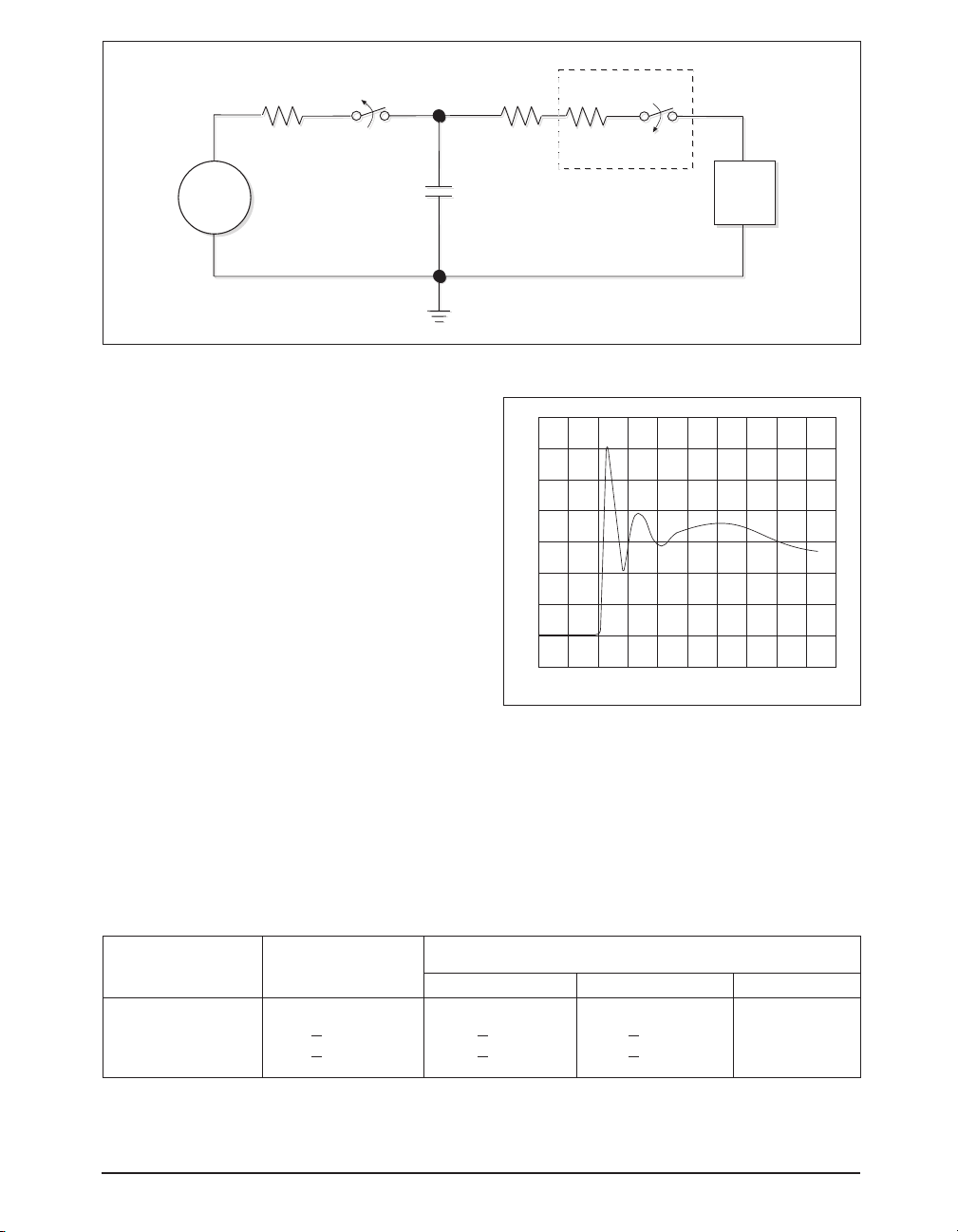
IEC1000-4-2 is shown on Figure 31. There are
two methods within IEC1000-4-2, the Air
Discharge method and the Contact Discharge
method.
With the Air Discharge Method, an ESD voltage
is applied to the equipment under test (EUT)
through air. This simulates an electrically charged
person ready to connect a cable onto the rear of
the system only to find an unpleasant zap just
before the person touches the back panel. The
high energy potential on the person discharges
through an arcing path to the rear panel of the
system before he or she even touches the system.
This energy, whether discharged directly or
through air, is predominantly a function of the
discharge current rather than the discharge
voltage. Variables with an air discharge such as
approach speed of the object carrying the ESD
potential to the system and humidity will tend to
change the discharge current. For example, the
rise time of the discharge current varies with the
approach speed.
The Contact Discharge Method applies the ESD
current directly to the EUT. This method was
devised to reduce the unpredictability of the
ESD arc. The discharge current rise time is
constant since the energy is directly transferred
without the air-gap arc. In situations such as
hand held systems, the ESD charge can be directly
discharged to the equipment from a person already
holding the equipment. The current is transferred
on to the keypad or the serial port of the equipment
directly and then travels through the PCB and finally
to the IC.
R
R
R
C
C
SW1
SW1
DC Power
Figure 30. ESD Test Circuit for Human Body Model
Date: 1/11/05 SP3243 +3.0V to +5.5V RS-232 Transceivers © Copyright 2005 Sipex Corporation
Source
R
S
S
SW2
SW2
C
C
S
S
Device
Under
Test
16
Page 17
R
S
and
R
V
add up to 330ΩΩ f f
or IEC1000-4-2.
Contact-Discharge Module
R
V
R
C
C
S
R
S
SW1
SW2
Contact-Discharge Module
Contact-Discharge Module
R
R
R
C
C
R
R
R
S
S
V
V
SW1
SW1
DC Power
Source
Figure 31. ESD Test Circuit for IEC1000-4-2
The circuit models in Figures30 and 31 represent
the typical ESD testing circuit used for all three
methods. The CS is initially charged with the DC
power supply when the first switch (SW1) is on.
Now that the capacitor is charged, the second
switch (SW2) is on while SW1 switches off. The
voltage stored in the capacitor is then applied
through RS, the current limiting resistor, onto the
device under test (DUT). In ESD tests, the SW2
switch is pulsed so that the device under test
receives a duration of voltage.
For the Human Body Model, the current limiting
resistor (RS) and the source capacitor (CS) are
1.5kΩ an 100pF, respectively. For IEC-1000-42, the current limiting resistor (RS) and the source
capacitor (CS) are 330Ω an 150pF, respectively.
SW2
SW2
C
C
S
S
RS and RV add up to 330Ω for IEC1000-4-2.
R
and
R
S
add up to 330
V
or IEC1000-4-2.
i ➙
30A
15A
0A
t=0ns t=30ns
t ➙
Figure 32. ESD Test Waveform for IEC1000-4-2
Device
Under
Test
The higher CS value and lower RS value in the
IEC1000-4-2 model are more stringent than the
Human Body Model. The larger storage capacitor
injects a higher voltage to the test point when
SW2 is switched on. The lower current limiting
resistor increases the current charge onto the test
point.
DEVICE PIN HUMAN BODY IEC1000-4-2
TESTED MODEL Air Discharge Direct Contact Level
Driver Outputs +15kV +15kV +8kV 4
Receiver Inputs
Table 4. Transceiver ESD Tolerance Levels
Date: 1/11/05 SP3243 +3.0V to +5.5V RS-232 Transceivers © Copyright 2005 Sipex Corporation
+15kV +15kV +8kV 4
17
Page 18
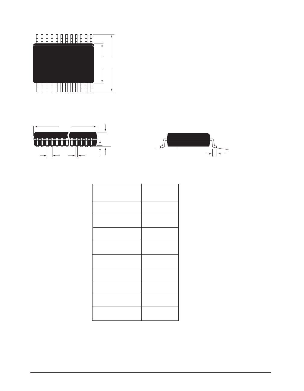
PACKAGE: PLASTIC
SMALL OUTLINE (SOIC)
(WIDE)
EH
D
A
Ø
Be
A1
DIMENSIONS (Inches)
Minimum/Maximum
(mm)
A
A1
B
D
E
e
H
L
Ø
28–PIN
0.090/0.104
(2.29/2.649)
0.004/0.012
(0.102/0.300)
0.013/0.020
(0.330/0.508)
0.697/0.713
(17.70/18.09)
0.291/0.299
(7.402/7.600)
0.050 BSC
(1.270 BSC)
0.394/0.419
(10.00/10.64)
0.016/0.050
(0.406/1.270)
0°/8°
(0°/8°)
L
Date: 1/11/05 SP3243 +3.0V to +5.5V RS-232 Transceivers © Copyright 2005 Sipex Corporation
18
Page 19
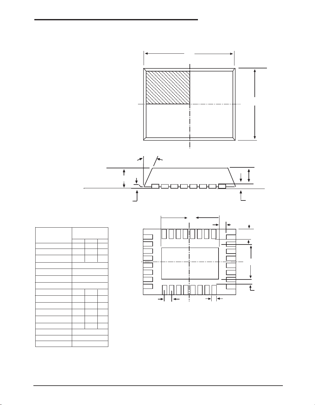
4X غ
PACKAGE: 32 PIN QFN
D
E
32 PIN QFN
JEDECMO220
(VHHD-4)
A
A1
A2
A3
D
E
e
b 0.18 0.25 0.30
Ø
D2
E2
L
K
N
ND
NE
MIN NOM MAX
0.80 0.90 1.00
0 0.02 0.05
0 0.65 1.00
0º - 14º
3.50 3.65 3.80
3.50 3.65 3.80
0.35 0.40 0.45
0.20 - -
SEATING PLANE
Dimensions in
(mm)
0.20 REF
5.00 BSC
5.00 BSC
0.50 BSC
32
8
8
A
A1
A2
A3
D2
NX K
NX L
E2
NX K
e
NX b
32 PIN QFN
Date: 1/11/05 SP3243 +3.0V to +5.5V RS-232 Transceivers © Copyright 2005 Sipex Corporation
19
Page 20
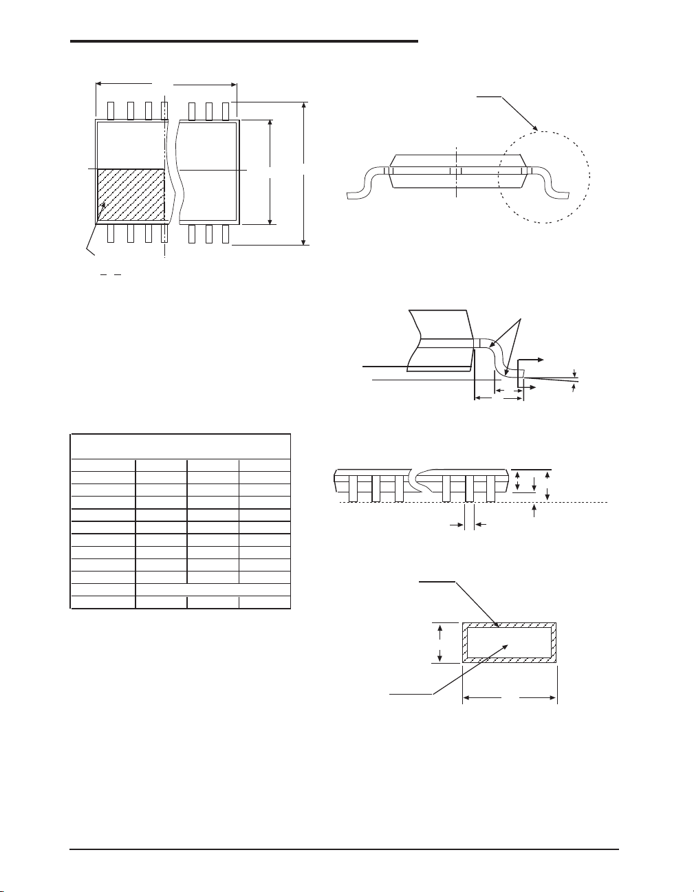
PACKAGE: 28 PIN SSOP
N
1
INDEX AREA
D
x
2
D
E1
2
E1
2
28 Pin SSOP JEDEC MO-150 (AH) Variation
SYMBOL
MIN NOM MAX
A--2
A1 0.05 - A2 1.65 1.75 1.85
b 0.22 - 0.38
c 0.09 - 0.25
D 9.9 10.2 10.5
E 7.4 7.8 8.2
E1 5 5.3 5.6
L 0.55 0.75 0.95
L1
1.25 REF
ø0º4º8º
E
Gauge Plane
Seaing Plane
WITH LEAD FINISH
SEE DETAIL “A”
b
L
L1
DETAIL A
2 NX R R1
A
A2
A1
A
Ø
A
Seating Plane
Note: Dimensions in (mm)
c
BASE METAL
b
Section A-A
Date: 1/11/05 SP3243 +3.0V to +5.5V RS-232 Transceivers © Copyright 2005 Sipex Corporation
20
Page 21
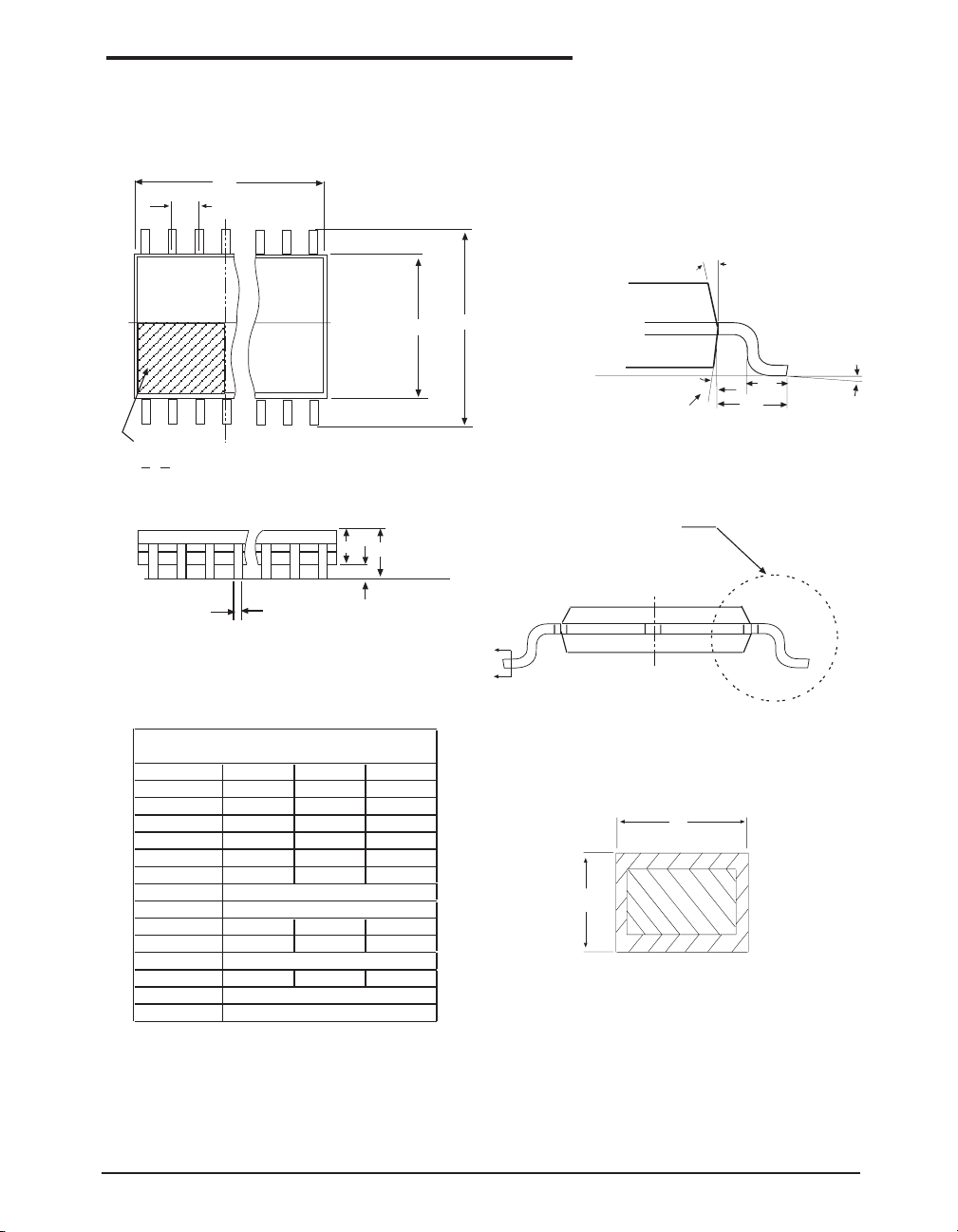
PACKAGE: 28 PIN TSSOP
D
e
Ø2
E
E1
12
INDEX AREA
D
E1
x
2
2
b
28 Pin TSSOP JEDEC MO-153 (AE)
Variation
SYMBOL
MIN NOM MAX
A--1.2
A1 0.05 - 0.15
A2 0.8 1 1.05
b 0.19 - 0.3
c 0.09 - 0.2
D 9.6 9.7 9.8
e
E
0.65 BSC
6.40 BSC
E1 4.3 4.4 4.5
L 0.45 0.6 0.75
L1
1.00 REF
Ø1 0º - 8º
Ø2
Ø3
12º REF
12º REF
Note: Dimensions in (mm)
A2
A1
A
Seating Plane
Seaing Plane
Ø3
L
L1
Ø1
DETAIL A
SEE DETAIL “A”
B
B
b
C
Section B-B
Date: 1/11/05 SP3243 +3.0V to +5.5V RS-232 Transceivers © Copyright 2005 Sipex Corporation
21
Page 22
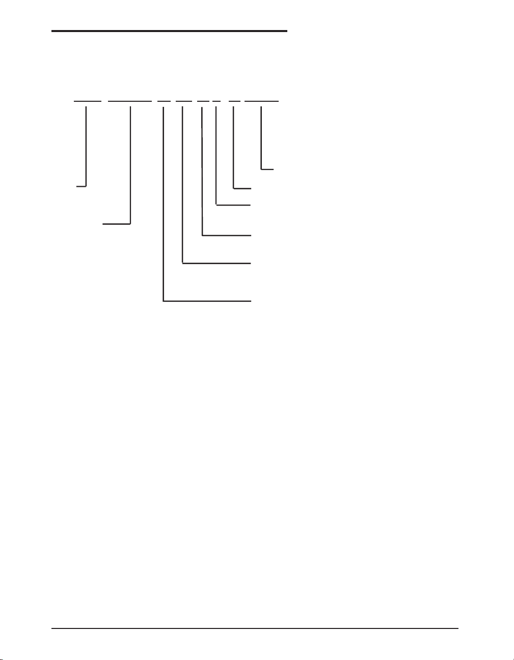
SP 3243 E U EY L /TR
PRODUCT NOMENCLATURE
Tape and Reel options
Sipex
Part Number
“L” suffix indicates Lead Free packaging
Package Type A= SSOP
Temperature Range C= Commercial Range 0ºC to 70ºC
Speed Indicator Blank= 120Kbps
ESD Rating E= 15kV HBM and IEC 1000-4
P= PDIP
Y=TSSOP
E= Extended Range -40ºC to 85ºC
B= 250Kbps
H= 450Kbps
U= 1Mbps
Date: 1/11/05 SP3243 +3.0V to +5.5V RS-232 Transceivers © Copyright 2005 Sipex Corporation
22
Page 23
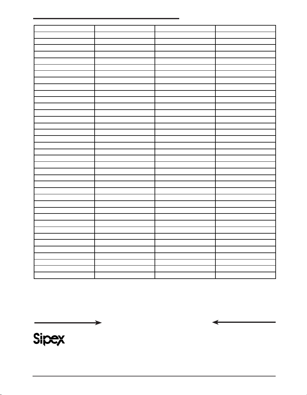
ORDERING INFORMATION
Part Number Speed (kbps) Temp Range Package
SP3243EBCA 250 -0 to 70C 28 Pin SSOP
SP3243EBCA/TR 250 -0 to 70C 28 Pin SSOP
SP3243EBCR
SP3243EBCR/TR
SP3243EBCT 250 -0 to 70C 28 Pin WSOIC
SP3243EBCT/TR 250 -0 to 70C 28 Pin WSOIC
SP3243EBCY
SP3243EBCY/TR
SP3243EBEA 250 -40 to 85C 28 Pin SSOP
SP3243EBEA/TR 250 -40 to 85C 28 Pin SSOP
SP3243EBET
SP3243EBET/TR
SP3243EBEY
SP3243EBEY/TR 250 -40 to 85C 28 Pin TSSOP
SP3243ECA 120 -0 to 70C 28 Pin SSOP
SP3243ECA/TR
SP3243ECT
SP3243ECT/TR 120 -0 to 70C 28 Pin WSOIC
SP3243EEA 120 -40 to 85C 28 Pin SSOP
SP3243EEA/TR
SP3243EET
SP3243EET/TR 120 -40 to 85C 28 Pin WSOIC
SP3243EUCA 1000 -0 to 70C 28 Pin SSOP
SP3243EUCA/TR 1000 -0 to 70C 28 Pin SSOP
SP3243EUCR
SP3243EUCR/TR
SP3243EUCT 1000 -0 to 70C 28 Pin WSOIC
SP3243EUCT/TR 1000 -0 to 70C 28 Pin WSOIC
SP3243EUCY
SP3243EUCY/TR
SP3243EUEA 1000 -40 to 85C 28 Pin SSOP
SP3243EUEA/TR 1000 -40 to 85C 28 Pin SSOP
SP3243EUER
SP3243EUER/TR
SP3243EUET 1000 -40 to 85C 28 Pin WSOIC
SP3243EUET/TR 1000 -40 to 85C 28 Pin WSOIC
SP3243EUEY 1000 -40 to 85C 28 Pin TSSOP
SP3243EUEY/TR
Available in lead free packaging. To order add “-L” suffix to part number.
Example: SP3243EUEA/TR = standard; SP3243EUEA-L/TR = lead free
/TR = Tape and Reel
Pack quantity is 1,500 for SSOP, TSSOP and WSOIC.
250 -0 to 70C 32 Pin QFN
250 -0 to 70C 32 Pin QFN
250 -0 to 70C 28 Pin TSSOP
250 -0 to 70C 28 Pin TSSOP
250 -40 to 85C 28 Pin WSOIC
250 -40 to 85C 28 Pin WSOIC
250 -40 to 85C 28 Pin TSSOP
120 -0 to 70C 28 Pin SSOP
120 -0 to 70C 28 Pin WSOIC
120 -40 to 85C 28 Pin SSOP
120 -40 to 85C 28 Pin WSOIC
1000 -0 to 70C 32 Pin QFN
1000 -0 to 70C 32 Pin QFN
1000 -0 to 70C 28 Pin TSSOP
1000 -0 to 70C 28 Pin TSSOP
1000 -40 to 85C 32 Pin QFN
1000 -40 to 85C 32 Pin QFN
1000 -40 to 85C 28 Pin TSSOP
CLICK HERE TO ORDER SAMPLES
Sipex Corporation
Corporation
ANALOG EXCELLENCE
Date: 1/11/05 SP3243 +3.0V to +5.5V RS-232 Transceivers © Copyright 2005 Sipex Corporation
Headquarters and
Sales Office
233 South Hillview Drive
Milpitas, CA 95035
TEL: (408) 934-7500
FAX: (408) 935-7600
23
Page 24
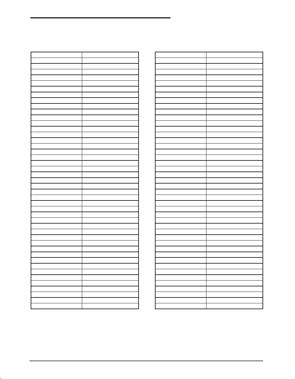
ORDERING INFORMATION
Contact factory for availability of the following legacy part numbers. For long term availability
Sipex recommends upgrades as listed below. All upgrade part numbers shown are fully pinout
and function compatible with legacy part numbers. Upgrade part numbers may contain
feature and/or performance enhancements or other changes to datasheet parameters.
Legacy Part Number Recommended Upgrade Legacy Part Number Recommended Upgrade
SP3243BCA SP3243EBCA SP3243EHCA SP3243EUCA
SP3243BCA/TR SP3243EBCA/TR SP3243EHCA/TR SP3243EUCA/TR
SP3243BCA-L SP3243EBCA-L SP3243EHCT SP3243EUCT
SP3243BCA-L/TR SP3243EBCA-L/TR SP3243EHCT/TR SP3243EUCT/TR
SP3243BCR SP3243EBCR SP3243HCA SP3243EUCA
SP3243BCR/TR SP3243EBCR/TR SP3243HCA/TR SP3243EUCA/TR
SP3243BCR-L SP3243EBCR-L SP3243HCA-L SP3243EUCA-L
SP3243BCR-L/TR SP3243EBCR-L/TR SP3243HCA-L/TR SP3243EUCA-L/TR
SP3243BCT SP3243EBCT SP3243HCT SP3243EUCT
SP3243BCT/TR SP3243EBCT/TR SP3243HCT/TR SP3243EUCT/TR
SP3243BCT-L SP3243EBCT-L SP3243HCT-L SP3243EUCT-L
SP3243BCT-L/TR SP3243EBCT-L/TR SP3243HCT-L/TR SP3243EUCT-L/TR
SP3243BCY SP3243EBCY SP3243UCA SP3243EUCA
SP3243BCY/TR SP3243EBCY/TR SP3243UCA/TR SP3243EUCA/TR
SP3243BCY-L SP3243EBCY-L SP3243UCA-L SP3243EUCA-L
SP3243BCY-L/TR SP3243EBCY-L/TR SP3243UCA-L/TR SP3243EUCA-L/TR
SP3243BEA SP3243EBEA SP3243UCR SP3243EUCR
SP3243BEA/TR SP3243EBEA/TR SP3243UCR/TR SP3243EUCR/TR
SP3243BEA-L SP3243EBEA-L SP3243UCR-L SP3243EUCR-L
SP3243BEA-L/TR SP3243EBEA-L/TR SP3243UCR-L/TR SP3243EUCR-L/TR
SP3243BET SP3243EBET SP3243UCT SP3243EUCT
SP3243BET/TR SP3243EBET/TR SP3243UCT/TR SP3243EUCT/TR
SP3243BET-L SP3243EBET-L SP3243UCT-L SP3243EUCT-L
SP3243BET-L/TR SP3243EBET-L/TR SP3243UCT-L/TR SP3243EUCT-L/TR
SP3243BEY SP3243EBEY SP3243UCY SP3243EUCY
SP3243BEY/TR SP3243EBEY/TR SP3243UCY/TR SP3243EUCY/TR
SP3243BEY-L SP3243EBEY-L SP3243UCY-L SP3243EUCY-L
SP3243BEY-L/TR SP3243EBEY-L/TR SP3243UCY-L/TR SP3243EUCY-L/TR
SP3243CA SP3243ECA SP3243UEA SP3243EUEA
SP3243CA/TR SP3243ECA/TR SP3243UEA/TR SP3243EUEA/TR
SP3243CA-L SP3243ECA-L SP3243UEA-L SP3243EUEA-L
SP3243CA-L/TR SP3243ECA-L/TR SP3243UEA-L/TR SP3243EUEA-L/TR
SP3243CT SP3243ECT SP3243UER SP3243EUER
SP3243CT/TR SP3243ECT/TR SP3243UER/TR SP3243EUER/TR
SP3243CT-L SP3243ECT-L SP3243UER-L SP3243EUER-L
SP3243CT-L/TR SP3243ECT-L/TR SP3243UER-L/TR SP3243EUER-L/TR
SP3243EA SP3243EEA SP3243UET SP3243EUET
SP3243EA/TR SP3243EEA/TR SP3243UET/TR SP3243EUET/TR
SP3243EA-L SP3243EEA-L SP3243UET-L SP3243EUET-L
SP3243EA-L/TR SP3243EEA-L/TR SP3243UET-L/TR SP3243EUET-L/TR
SP3243ET SP3243EET SP3243UEY SP3243EUEY
SP3243ET/TR SP3243EET/TR SP3243UEY/TR SP3243EUEY/TR
SP3243ET-L SP3243EET-L SP3243UEY-L SP3243EUEY-L
SP3243ET-L/TR SP3243EET-L/TR SP3243UEY-L/TR SP3243EUEY-L/TR
Date: 1/11/05 SP3243 +3.0V to +5.5V RS-232 Transceivers © Copyright 2005 Sipex Corporation
24
 Loading...