

Page 1
TVS Diode Arrays (SPA
Pin 1 and 8
Pi
an
Line out
Line out
RoHS
GREEN
®
Diodes)TVS Diode Arrays (SPA® Diodes)
Lightning Surge Protection - SP2502L Series
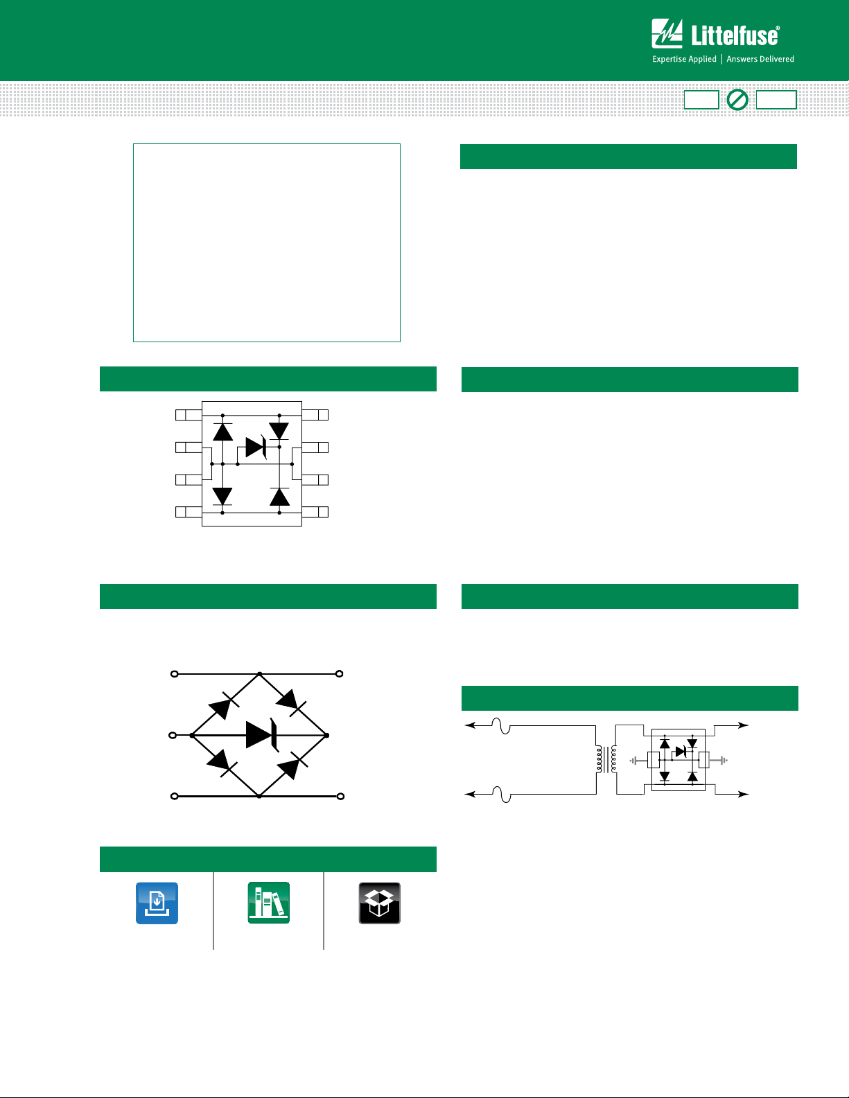
SP2502L Series 3.3V 75A Diode Array
Pinout
1
2
3
SOIC-8 (Top View)
Note: Pinout diagrams above shown as device footprint on circuit board.
8
7
6
54
Pb
Description
The SP2502L provides overvoltage protection for
applications such as 10/100/1000 Base-T Ethernet and T3/
E3 interfaces. This device has a low capacitance of only
5pF making it suitable for PHY side Ethernet protection
and the capability to protect against both longitudinal and
differential transients. Furthermore, the SP2502L is rated
up to 100A (tp=2/10µs) making it suitable for line side
protection as well against lightning transients as defined
by GR-1089 (intra-building), ITU, YD/T, etc. The application
schematic provides the connection information for a PHY
side protection scheme of a single differential pair.
Features
• Lightning protection,
IEC61000-4-5, 75A
(8/20µs)
• Low clamping voltage
• Low insertion loss, loglinear capacitance
• Combined longitudinal
and metallic protection
• Clamping speed of
nanoseconds
• SOIC-8 surface mount
package (JEDEC MS-012)
• UL 94V-0 epoxy molding
• RoHS compliant
Functional Block Diagram
Line in
n 2, 3, 6,
d 7
Line in
Pin 4 and 5
Additional Information
Datasheet
Life Support Note:
Not Intended for Use in Life Support or Life Saving Applications
The products shown herein are not designed for use in life sustaining or life saving
applications unless otherwise expressly indicated.
© 2013 Littelfuse, Inc.
Specifications are subject to change without notice.
Revised: 04/24/13
Resources
Samples
Applications
• T1/E1 Line cards
• 10/100/1000 BaseT
• T3/E3 and DS3 Interfaces
• STS-1 Interfaces
Ethernet
Application Example
TeleLink (0461 1.25)
1
2
3
4
SP2502L
8
7
6
5
to chipset
(Ethernet PHY,
T3/E3 PHY, etc.)
The schematic shows protection for a single differential
pair as part of a larger high-speed data interface such as
Ethernet. The SP2502L provides both metallic (differential)
and longitudinal (common mode) protection from lightning
induced surge events as specified by regulatory standards
such as Telcordia’s GR-1089 CORE and ITU K.20 and 21.
The SP2502L protects against both positive and negative
induced surge events while the TeleLink fuse provides
overcurrent protection for the long term 50/60 Hz power
fault events.
Page 2
®
TVS Diode Arrays (SPA
®
Diodes)TVS Diode Arrays (SPA
Diodes)
Lightning Surge Protection - SP2502L Series
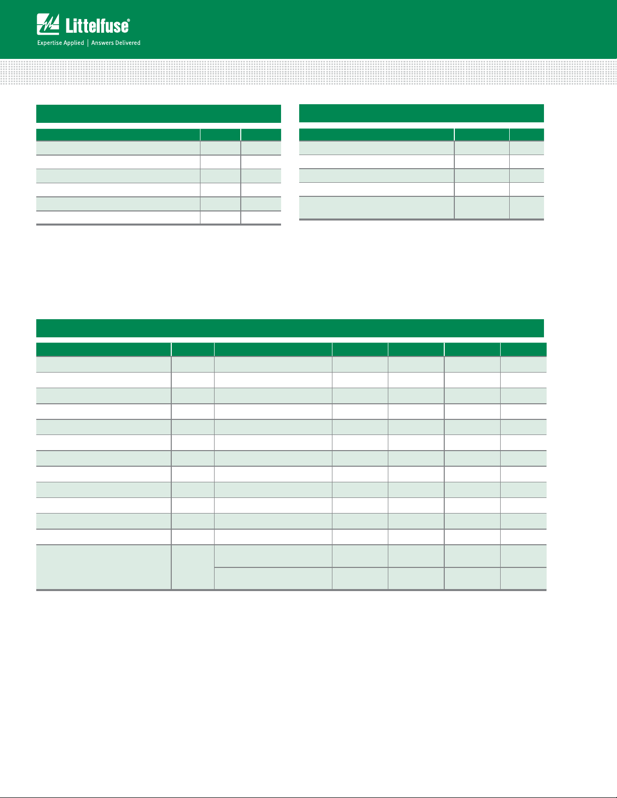
Absolute Maximum Ratings
Parameter Rating Units
Peak Pulse Current (8/20µs) 75 A
Peak Pulse Power (8/20µs) 210 0 W
IEC 61000-4-2, Direct Discharge, (Level 4) 30 kV
IEC 61000-4-2, Air Discharge, (Level 4) 30 kV
Telcordia GR 1089 (Intra-Building) (2/10µs) 100 A
ITU K.20 (5/310µs) 20 A
CAUTION: Stresses above those listed in “Absolute Maximum Ratings” may cause
permanent damage to the device. This is a stress only rating and operation of the device
at these or any other conditions above those indicated in the operational sections of this
specification is not implied.
Electrical Characteristics (TOP = 25°C)
Parameter Symbol Test Conditions Min Typ Max Units
Reverse Stand-Off Voltage V
Reverse Breakdown Voltage V
Snap Back Voltage V
Reverse Leakage Current I
1
Clamping Voltage, Line-Ground
Clamping Voltage, Line-Ground
Clamping Voltage, Line-Ground
Dynamic Resistance, Line-Ground
Clamping Voltage, Line-Line
Clamping Voltage, Line-Line
Clamping Voltage, Line-Line
Dynamic Resistance, Line-Line
Junction Capacitance
1
V
1
V
1
V
1
1
1
1
1
R
R
RWM
BR
SB
R
C
C
C
DYN
V
C
V
C
V
C
DYN
C
j
Line to Line, V
IT≤1µA - - 3.3 V
IT= 2µA 3.3 - - V
IT= 50mA 3.3 - - V
V
RWM
IPP= 40A, tp=8/20 µs - - 14 V
IPP= 75A, tp=8/20 µs - - 20 V
IPP= 100A, tp=2/10 µs 20 V
( VC2-VC1)/(I
IPP= 40A, tp=8/20 µs - - 20 V
IPP= 75A, tp=8/20 µs - - 30 V
IPP= 100A, tp=2/10 µs 30 V
( VC2-VC1)/(I
Line to Ground
VR=0V, f= 1MHz
Thermal Information
Parameter Rating Units
SOIC Package 170 °C/W
Operating Temperature Range –40 to 125 °C
Storage Temperature Range –55 to 150 °C
Maximum Junction Temperature 150 °C
Maximum Lead Temperature (Soldering
20-40s) (SOIC - Lead Tips Only)
= 3.3V - - 1 µA
) - 0.2 -
PP2-IPP1
) - 0.3 -
PP2-IPP1
- 5 8 pF
=0V, f= 1MHz - 2.5 5 pF
R
260 °C
SP4040
W
W
1
Parameter is guaranteed by design and/or device characterization.
Specifications are subject to change without notice.
© 2013 Littelfuse, Inc.
Revised: 04/24/13
Page 3
TVS Diode Arrays (SPA
0
5
10
15
20
25
30
010203040506070
Clamp Voltage-V
C
(V)
Peak Pulse Current-IPP(A)
Line-Line
Line-Gound
0.0
1.0
2.0
3.0
4.0
5.0
Bias Voltage (V)
Capacitance (pF)
Line-Line
Line-Gound
0.0 0.5 1.0 1.5 2.0 2.5 3.0
6.0
0.1
1
10
110100 1000
Peak Pulse Power (kW)
Peak Pulse Duraon
-tP(µs)
Ambient Temperature (ºC)
Percentage of Rated Current (% I
P
)
0 10 20 30 40 50 60 70 80 90 100 110 120 130 140 150
0
20
40
60
80
100
120
®
Diodes)TVS Diode Arrays (SPA® Diodes)
Lightning Surge Protection - SP2502L Series
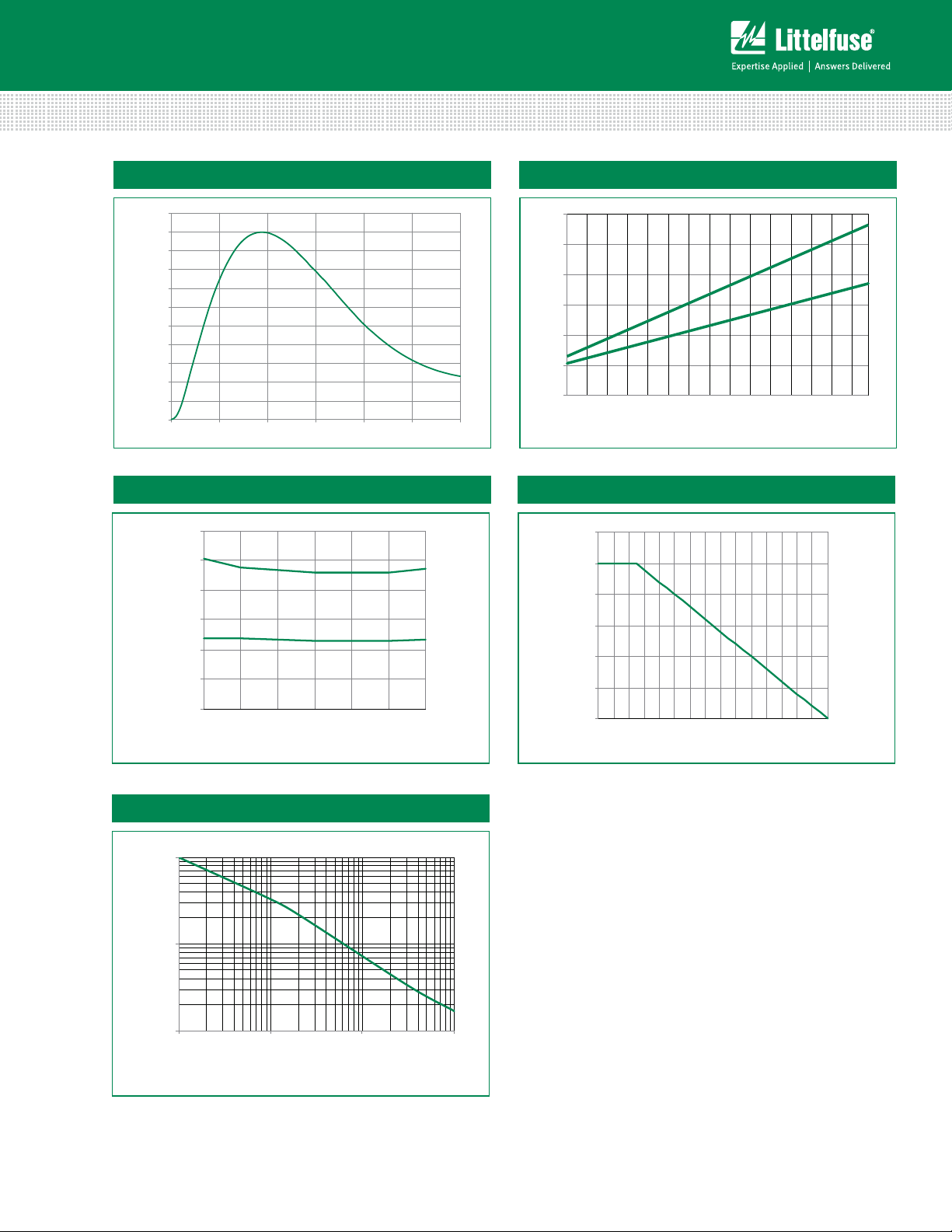
Pulse Waveform
110%
100%
90%
80%
70%
PP
60%
50%
Percent of I
40%
30%
20%
10%
0%
0.0 5.0 10.0 15.0 20.0 25.0 30.0
Capacitance vs. Reverse Bias at 1MHz
Clamping Voltage vs. I
Current Derating Curve
PP
Non-Repetitive Peak Pulse Power vs. Pulse Time
© 2013 Littelfuse, Inc.
Specifications are subject to change without notice.
Revised: 04/24/13
Page 4
SP
2502L
B T
G
Series
Package
B = SOIC-8
T= Tape & Reel
G= Green
TVS Diode Arrays
(SPA
®
Diodes)
t
R
R
o
C
e
T
L
T
P
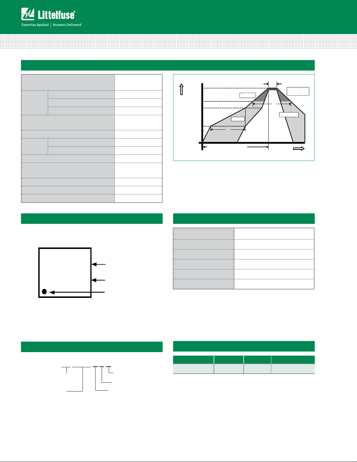
Soldering Parameters
Marking
F
L
SP2502
CYYWW
Date code
Pin1
®
TVS Diode Arrays (SPA
®
Diodes)TVS Diode Arrays (SPA
Diodes)
Lightning Surge Protection - SP2502L Series
Reflow Condition Pb – Free assembly
- Temperature Min (T
Pre Heat
Average ramp up rate (Liquidus) Temp
(T
) to peak
L
T
S(max)
Reflow
Peak Temperature (TP) 260
Time within 5°C of actual peak
Temperature (t
Ramp-down Rate 6°C/second max
Time 25°C to peak Temperature (T
Do not exceed 260°C
- Temperature Max (T
- Time (min to max) (ts) 60 – 180 secs
to TL - Ramp-up Rate 3°C/second max
- Temperature (TL) (Liquidus) 217°C
- Temperature (tL) 60 – 150 seconds
)
p
) 150°C
s(min)
) 200°C
s(max)
3°C/second max
+0/-5
°C
20 – 40 seconds
) 8 minutes Max.
P
Part Marking System
T
P
Ramp-up
t
amp-up
PreheatPrehea
S
T
L
T
S(max)
Temperature
T
S(min)
25
time to peak temperature
Product Characteristics
Lead Plating Matte Tin
Lead Material Copper Alloy
t
P
t
L
Critical Zone
ritical Zon
L to TP
to
T
Ramp-down
amp-d
Time
SP4040
Part Numbering System
Lead Coplanarity 0.0004 inches (0.102mm)
Substitute Material Silicon
Body Material Molded Epoxy
Flammability UL 94 V-0
Notes :
1. All dimensions are in millimeters
2. Dimensions include solder plating.
3. Dimensions are exclusive of mold flash & metal burr.
4. Blo is facing up for mold and facing down for trim/form, i.e. reverse trim/form.
5. Package surface matte finish VDI 11-13.
Ordering Information
Part Number Package Marking Min. Order Qty.
SP2502LBTG SOIC-8 SP2502 2500
Specifications are subject to change without notice.
© 2013 Littelfuse, Inc.
Revised: 04/24/13
Page 5
TVS Diode Arrays (SPA
User Feeding Direction
Pin 1 Location
®
Diodes)TVS Diode Arrays (SPA® Diodes)
Lightning Surge Protection - SP2502L Series
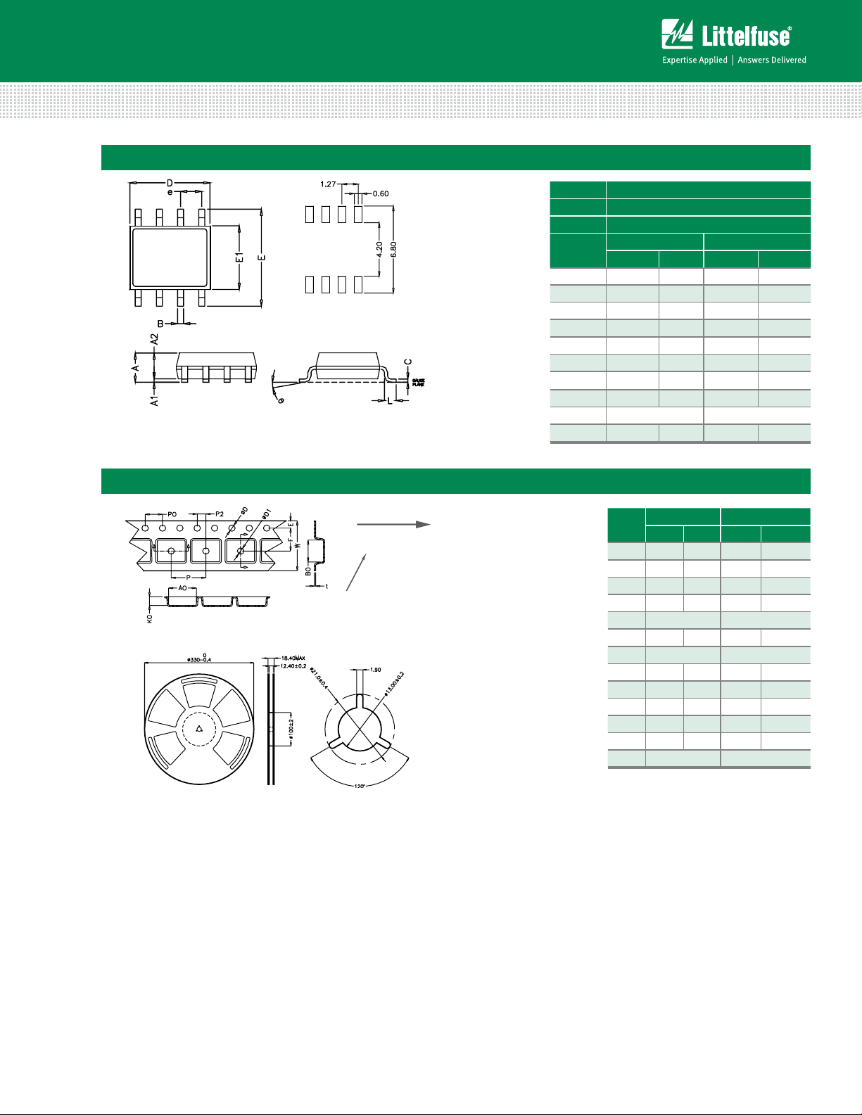
Package Dimensions — Mechanical Drawings and Recommended Solder Pad Outline
Package SOIC
Pins 8
JEDEC MS-012
F
L
o
Recommended
Soldering Pad Outline
(Reference Only)
A 1.35 1.75 0.053 0.069
A1 0.10 0.25 0.004 0. 010
A2 1.25 1.65 0.050 0.065
B 0.31 0.51 0.012 0.020
c 0.17 0.25 0.007 0 . 010
D 4.80 5.00 0.189 0.197
E 5.80
E1 3.80 4.00 0.150 0.157
e 1.27 BSC 0.050 BSC
L 0.40
Millimetres Inches
Min Max Min Max
6.20
1.27
0.228
0.016
0.244
0.050
Embossed Carrier Tape & Reel Specification — SOIC Package
Millimetres Inches
Min Max Min Max
E 1.65 1.85 0.065 0.073
F 5.4 5.6 0.213 0.22
P2 1.95 2.05 0.077 0.081
D 1. 5 1. 6 0.059 0.063
D1 1.50 Min 0.059 Min
P0 3.9 4.1 0.154 0.161
10P0 40.0 ± 0.20 1.574 ± 0.008
W 11. 9 12.1 0.468 0.476
P 7. 9 8.1 0.311 0.319
A0 6.3 6.5 0.248 0.256
B0 5.1 5.3 0.2 0.209
K0 2 2.2 0.079 0.087
t 0.30 ± 0.05 0.012 ± 0.002
© 2013 Littelfuse, Inc.
Specifications are subject to change without notice.
Revised: 04/24/13
 Loading...