

Page 1

TVS Diode Arrays (SPA
RoHS
GREEN
®
Diodes)
General Purpose ESD Protection - SP1005 Series
SP1005 Series 30pF 30kV Bidirectional Discrete TVS
Description
The SP1005 includes back-to-back Zener diodes fabricated
in a proprietary silicon avalanche technology to provide
protection for electronic equipment that may experience
destructive electrostatic discharges (ESD). These robust
diodes can safely absorb repetitive ESD strikes above the
maximum level specified in the IEC61000-4-2 international
standard (Level 4, ±8kV contact discharge) without
performance degradation. The back-to-back configuration
provides symmetrical ESD protection for data lines when
AC signals are present.
Pinout
0201 Flipchip
12
SOD882
Features
• ESD, IEC61000-4-2,
±30kV contact, ±30kV air
• EFT, IEC61000-4-4, 40A
(5/50ns)
• Lightning, IEC61000-4-5,
10A (t
=8/20μs)
P
• Low capacitance of 30pF
(@ V
=0V)
R
Pb
• Low leakage current of
0.1μA at 5V
• Space efcient 0201 and
0402 footprint
• AEC-Q101 qualied
(SOD882 package)
1
(AEC-Q101 qualified)
Functional Block Diagram
1
Additional Information
Datasheet
Resources
Applications
2
• Mobile Phones
• Smart Phones
• Camcorders
• Portable Medical
• Digital Cameras
• MP3/PMP
• Portable Navigation
Devices
• Tablets
• Point of Sale Terminals
Application Example
I/O Controller
ICP3
2
Samples
Outside
World
Keypads
P1
P2
P4
SP1005 (x4)
GND
Life Support Note:
Not Intended for Use in Life Support or Life Saving Applications
The products shown herein are not designed for use in life sustaining or life saving
applications unless otherwise expressly indicated.
© 2013 Littelfuse, Inc.
Specifications are subject to change without notice.
Revised: 11/22/13
Page 2
TVS Diode Arrays (SPA
0.0
5.0
10.0
15.0
20.0
25.0
30.0
35.0
40.0
0.0 0.5 1.01.5 2.0 2.5 3.0 3.5 4.0 4.5 5.0
Bias Voltage (V)
Capacitance (pF)
0%
10%
20%
30%
40%
50%
60%
70%
80%
90%
100%
110%
0.0 5.0 10.0 15.0 20.0 25.0 30.0
Time (μs)
Percent of I
PP
®
Diodes)
General Purpose ESD Protection - SP1005 Series
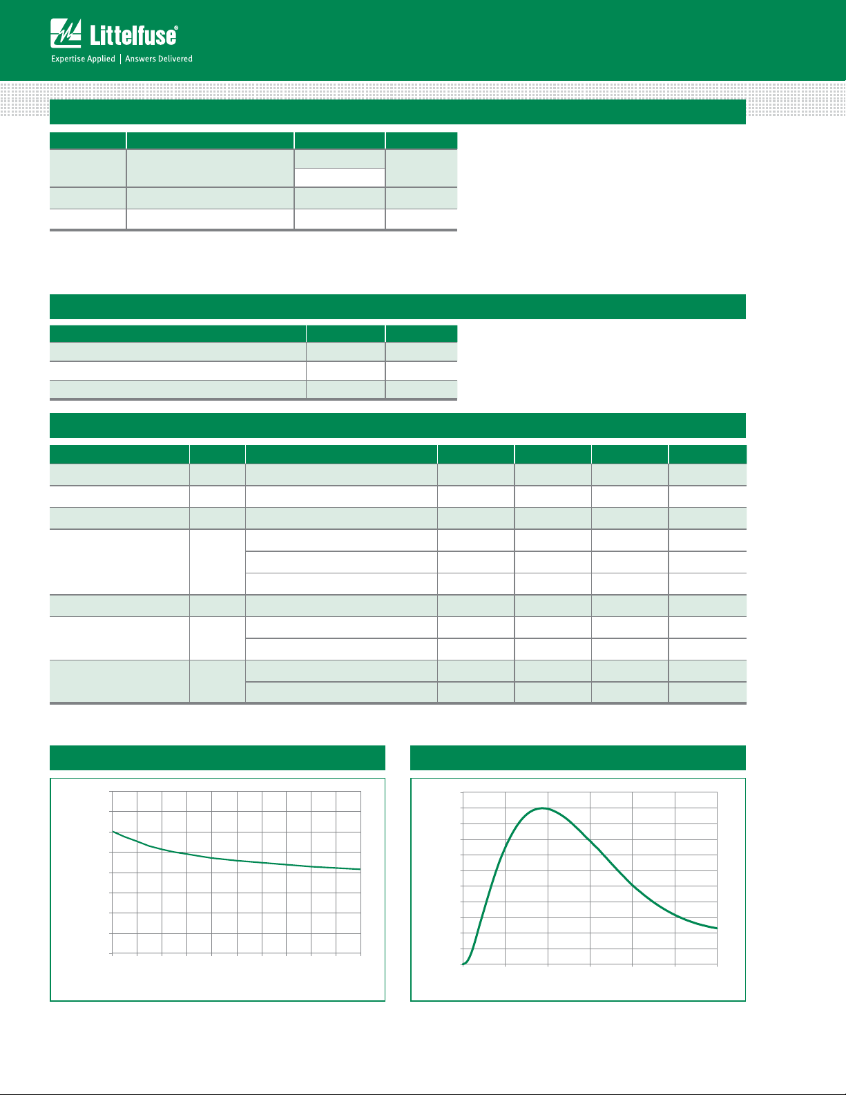
Absolute Maximum Ratings
Symbol Parameter Value Units
1
I
PP
T
OP
T
STOR
Notes:
1. “1 “ indicates SP1005-01WTG , while “2” indicates SP1005-01ETG
2. CAUTION: Stresses above those listed in “Absolute Maximum Ratings” may cause permanent damage to the device. This is a stress only rating and operation
of the device at these or any other conditions above those indicated in the operational sections of this specification is not implied.
Peak Current (tp=8/20μs)
Operating Temperature –40 to 125 °C
Storage Temperature –55 to 150 °C
Thermal Information
Parameter Rating Units
Storage Temperature Range –55 to 150 °C
Maximum Junction Temperature 150 °C
Maximum Lead Temperature (Soldering 20-40s) 260 °C
10.0
8.0
2
A
Electrical Characteristics (T
OP
=25ºC)
Parameter Symbol Test Conditions Min Typ Max Units
Reverse Standoff Voltage V
Breakdown Voltage V
Leakage Current I
Clamp Voltage
1
Dynamic Resistance R
ESD Withstand Voltage
Diode Capacitance
Note:
1
Parameter is guaranteed by design and/or device characterization.
1
1
V
RWM
BR
LEAK
V
DYN
ESD
C
C
IEC61000-4-2 (Contact Discharge) ±30 kV
IEC61000-4-2 (Air Discharge) ±30 kV
D
6.0 V
IR=1mA 8.5 9.5 V
VR=5V with 1 pin at GND 0.1 0.5 μA
IPP=1A, tp=8/20µs, Fwd 9.3 V
I
=2A, tp=8/20µs, Fwd 10.0 V
PP
I
=10A, tP=8/20μs, Fwd 15.6 V
PP
(VC2 - VC1) / (I
- I
) 0.7 Ω
PP2
PP1
Reverse Bias=0V 30 pF
Reverse Bias=2.5V 23 pF
Pulse WaveformCapacitance vs. Reverse Bias
Specifications are subject to change without notice.
© 2013 Littelfuse, Inc.
Revised: 11/22/13
Page 3
TVS Diode Arrays (SPA
0.0
2.0
4.0
6.0
8.0
10.0
12.0
14.0
16.0
18.0
1.0 2.0 3.0 4.0 5.0 6.0 7. 0 8.0 9.0 10.0
Peak Pulse Current-I
PP
(A)
Clamp Voltage (V
C
)
-35
-30
-25
-20
-15
-10
-5
0
5
110100 1000 10000
Frequency (MHz)
Attenuation (dB)
t
R
R
o
C
e
T
T
®
Diodes)
General Purpose ESD Protection - SP1005 Series
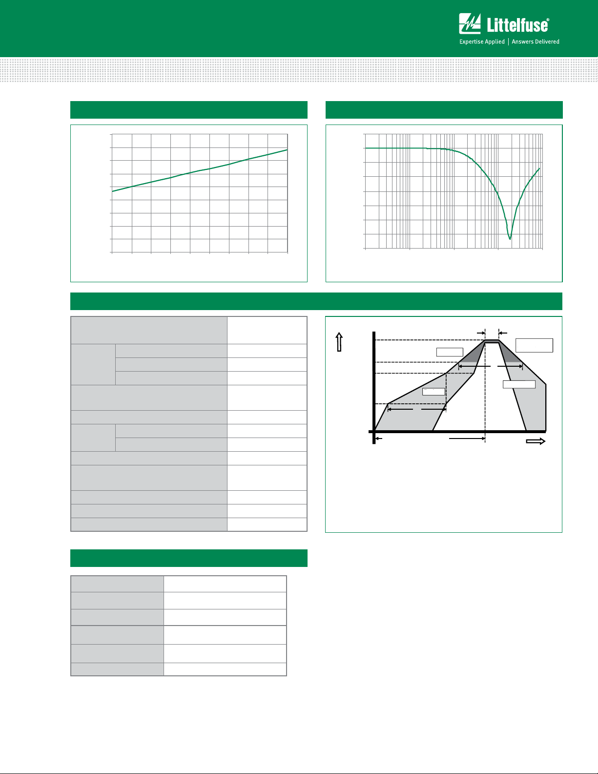
Clamping Voltage vs. I
PP
Soldering Parameters
Reflow Condition Pb – Free assembly
- Temperature Min (T
Pre Heat
- Temperature Max (T
- Time (min to max) (ts) 60 – 180 secs
Average ramp up rate (Liquidus) Temp
(T
) to peak
L
to TL - Ramp-up Rate 3°C/second max
T
S(max)
Reflow
- Temperature (TL) (Liquidus) 217°C
- Temperature (tL) 60 – 150 seconds
Peak Temperature (TP) 260
Time within 5°C of actual peak
Temperature (t
)
p
Ramp-down Rate 6°C/second max
Time 25°C to peak Temperature (T
Do not exceed 260°C
) 150°C
s(min)
) 200°C
s(max)
3°C/second max
+0/-5
°C
20 – 40 seconds
) 8 minutes Max.
P
Insertion Loss (S21) I/O to GND
T
P
Ramp-up
t
amp-up
PreheatPrehea
S
T
L
T
S(max)
Temperature
T
S(min)
25
time to peak temperature
t
P
t
L
Critical Zone
ritical Zon
T
L to TP
to
Ramp-down
amp-d
Time
Product Characteristics of SOD-882 Package
Lead Plating Pre-Plated Frame
Lead Material Copper Alloy
Lead Coplanarity 0.0004 inches (0.102mm)
Substitute Material Silicon
Body Material Molded Epoxy
Flammability UL 94 V-0
Notes :
1. All dimensions are in millimeters
2. Dimensions include solder plating.
3. Dimensions are exclusive of mold flash & metal burr.
4. Blo is facing up for mold and facing down for trim/form, i.e. reverse trim/form.
5. Package surface matte finish VDI 11-13.
© 2013 Littelfuse, Inc.
Specifications are subject to change without notice.
Revised: 11/22/13
Page 4
TVS Diode Arrays (SPA
A
B
D
E
D
F
C
G
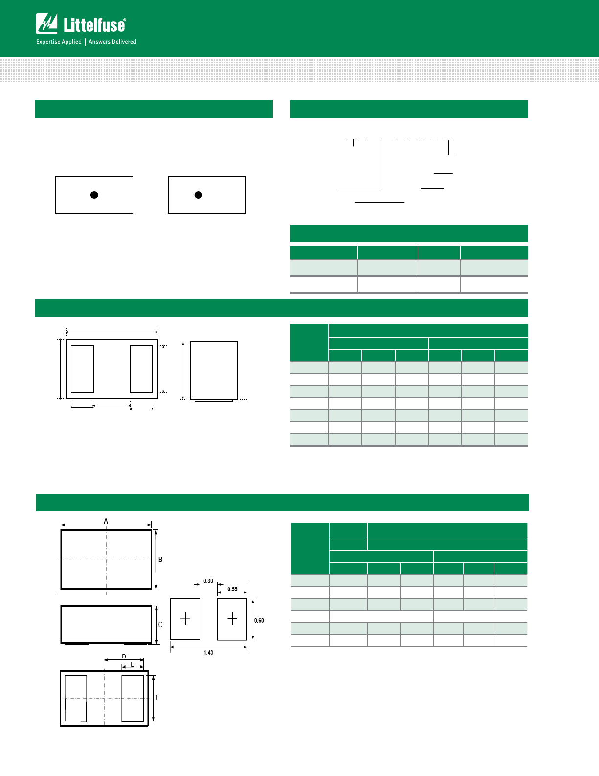
Recommended Soldering Pad Layout
®
Diodes)
General Purpose ESD Protection - SP1005 Series
Part Marking System
SP1005-01WTG
SP1005-01ETG
Package Dimensions — 0201 Flipchip
Part Numbering System
1005 01
SP
TVS Diode Arrays
®
(SPA
Diodes)
a
Series
Number of
Channels
T
G
G= Green
T= Tape & Reel
Package
W: 0201 Flipchip
E: SOD882
x
–
Ordering Information
Part Number Package Marking Min. Order Qty.
SP1005-01WTG 0201 Flipchip • 10,000
SP1005-01ETG SOD882 •a 10,000
0201 Flipchip
Symbol
A 0.595 0.620 0.645 0.0234 0.0244 0.0254
B 0.295 0.320 0.345 0.0116 0.0126 0.0136
C 0.245 0.275 0.305 0.0096 0.0108 0.0120
D 0.145 0.150 0.155 0.0057 0.0059 0.0061
E 0.245 0.250 0.255 0.0096 0.0098 0.010 0
F 0.245 0.250 0.255 0.0096 0.0098 0 . 0100
G 0.005 0. 010 0.015 0.0002 0.0004 0.0006
Millimeters Inches
Min Typ Max Min Typ Max
Package Dimensions — SOD882
Package SOD882
Symbol
JEDEC MO-236
Millimeters Inches
Min Typ Max Min Typ Max
A 0.90 1. 0 0 1. 1 0 0.035 0.039 0.043
B 0.50 0.60 0.70 0.020 0.024 0.028
C 0.40 0.50 0.60 0.016 0.020 0.024
D 0.45 0.018
E 0.20 0.25 0.35 0.008 0.010 0.012
F 0.45 0.50 0.55 0.018 0.020 0.022
Specifications are subject to change without notice.
© 2013 Littelfuse, Inc.
Revised: 11/22/13
Page 5
TVS Diode Arrays (SPA
0.28
0.30
0.75
0.19
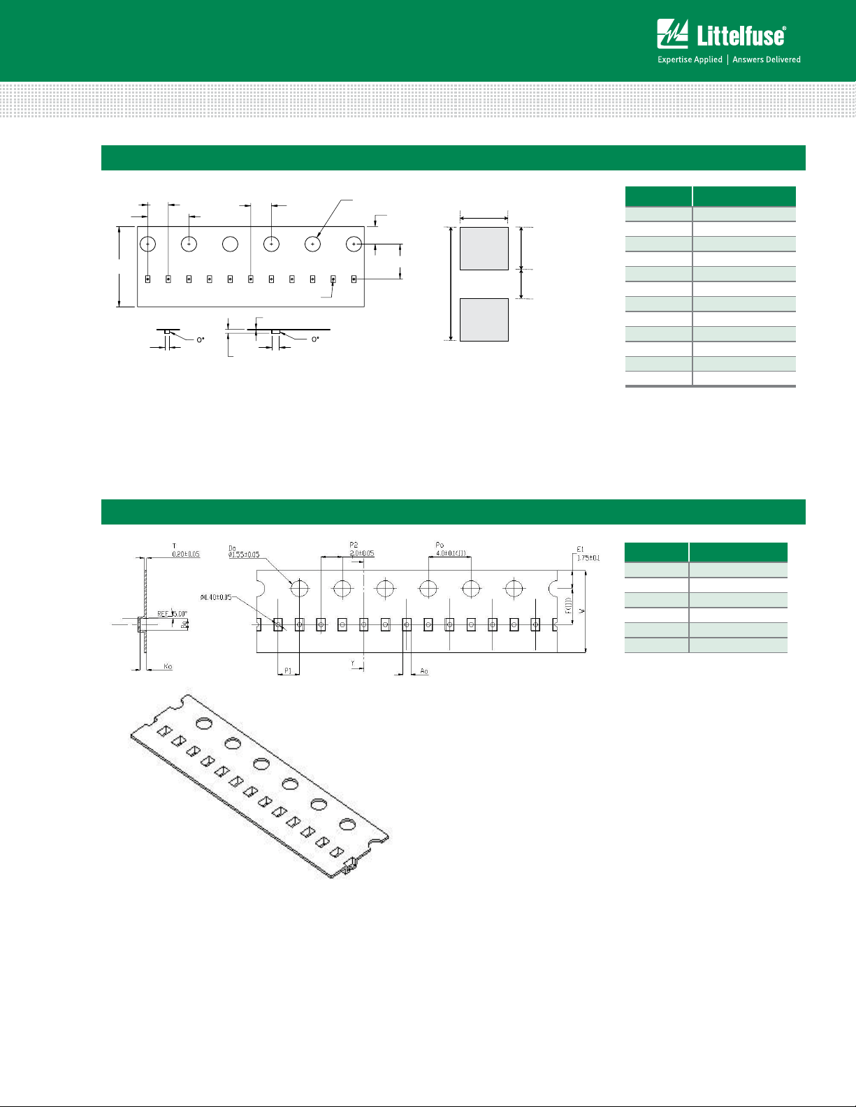
Recommended Solder Pad Footprint
A0
K0
B0
T
P0
P1
P2
D
D1
E
F
W
*Sizes in mm
®
Diodes)
General Purpose ESD Protection - SP1005 Series
Embossed Carrier Tape & Reel Specification — 0201 Flipchip
Symbol Millimeters
A0 0.41±0.03
B0 0.70±0.03
D ø 1.50 + 0.10
D1 ø 0.20 ± 0.05
E 1.75±0.10
F 3.50±0.05
K0 0.38±0.03
P0 2.00±0.05
P1 2.00±0.05
P2 4.00±0.10
W 8.00 + 0.30 -0.10
T 0.23±0.02
Embossed Carrier Tape & Reel Specification — SOD882
Symbol Millimeters
A0 0.70±0.045
B0 1.10±0.045
K0 0.65±0.045
F 3.50±0.05
P1 2.00±0.10
W 8.00 + 0.30 -0.10
© 2013 Littelfuse, Inc.
Specifications are subject to change without notice.
Revised: 11/22/13
Page 6

TVS Diode Arrays (SPA
®
Diodes)
General Purpose ESD Protection - SP1005 Series
Specifications are subject to change without notice.
© 2013 Littelfuse, Inc.
Revised: 11/22/13
 Loading...