

Page 1
SIPMOS Small-Signal Transistor SP 0610L
● V
● I
D
● R
● P channel
● Enhancement mode
DS
DS(on)
− 60 V
− 0.18 A
10 Ω
2
3
1
Type Ordering Code Tape and Reel
Information
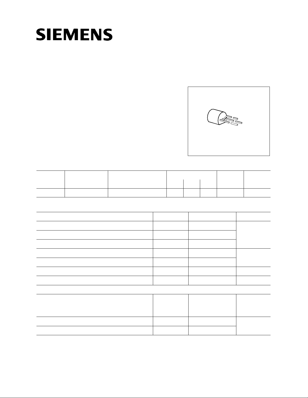
Pin Configuration Marking Package
123
SP 0610 L Q67000-S065 bulk D G S SP0610L TO-92
Maximum Ratings
Parameter Symbol Values Unit
Drain-source voltage
Drain-gate voltage,
R
= 20 kΩ V
GS
Gate-source voltage
Continuous drain current,
Pulsed drain current,
Max. power dissipation,
T
= 25 ˚C I
A
T
= 25 ˚C I
A
T
= 25 ˚C P
A
Operating and storage temperature range
V
V
D
D puls
T
DS
DGR
GS
tot
, T
j
stg
− 60 V
− 60
± 20
− 0.18 A
− 0.72
0.63 W
− 55 … + 150 ˚C
Thermal resistance, chip-ambient
R
thJA
≤ 200
(without heat sink)
R
thJSR
–
DIN humidity category, DIN 40 040 – E –
IEC climatic category, DIN IEC 68-1 – 55/150/56
K/W
Page 2
SP 0610L
Electrical Characteristics
T
= 25 ˚C, unless otherwise specified.
at
j
Parameter Symbol Values Unit
min. typ. max.
Static Characteristics
Drain-source breakdown voltage
V
= 0, ID = 0.25 mA
GS
Gate threshold voltage
V
= VDS, ID = 1 mA
GS
Zero gate voltage drain current
V
= − 60 V, VGS = 0
DS
T
= 25 ˚C
j
Gate-source leakage current
V
= − 20 V, VDS = 0
GS
Drain-source on-resistance
V
= − 10 V, ID = − 0.5 A
GS
Dynamic Characteristics
Forward transconductance
V
≥ 2 × ID× R
DS
DS(on)max
, ID = − 0.5 A
Input capacitance
V
= 0, VDS = − 25 V, f = 1 MHz
GS
Output capacitance
V
= 0, VDS = − 25 V, f = 1 MHz
GS
Reverse transfer capacitance
V
= 0, VDS = − 25 V, f = 1 MHz
GS
Turn-on time
V
= − 30V, VGS = −10V, RGS =50Ω,
DD
I
= − 0.27A
D
Turn-off time
V
= − 30V, VGS = −10V, RGS =50Ω,
DD
I
= − 0.27A
D
t
, (ton = t
on
t
, (t
off
+ tr)
d(on)
= t
d(off)
+ tf)
off
V
(BR)DSS
V
GS(th)
I
DSS
I
GSS
R
DS(on)
g
fs
C
iiss
C
oss
C
rss
t
d(on)
t
r
t
d(off)
t
f
V
− 60 – –
− 1.0 − 1.5 − 2.0
µA
– − 0.1 − 1
nA
– − 1 − 10
Ω
–710
S
0.08 0.13 –
pF
–3040
–1725
–812
– 7 10 ns
–1218
–1013
–2027
Page 3

SP 0610L
Electrical Characteristics (cont’d)
at
T
= 25 ˚C, unless otherwise specified.
j
Parameter Symbol Values Unit
min. typ. max.
Reverse Diode
Continuous reverse drain current
T
= 25 ˚C
A
Pulsed reverse drain current
T
= 25 ˚C
A
Diode forward on-voltage
I
= − 0.18 A, VGS = 0
F
Package Outline
TO-92
I
S
A
––− 0.18
I
SM
––− 0.72
V
SD
V
– − 0.85 − 1.2
Dimensions in mm
Page 4

Characteristics
at
T
= 25 ˚C, unless otherwise specified.
j
P
Total power dissipation
= f (TA)
tot
Safe operating area ID = f (VDS)
parameter:
D = 0.01, T
= 25 ˚C
C
SP 0610L
Typ. output characteristics
parameter:
t
= 80 µs
p
I
= f (VDS)
D
Typ. drain-source on-resistance
R
= f (ID)
DS(on)
parameter:
V
GS
Page 5

SP 0610L
Typ. transfer characteristics ID = f (VGS)
parameter:
t
= 80 µs, VDS≥ 2 × ID× R
p
DS(on)max.
Typ. forward transconductance gfs= f (ID)
parameter:
V
≥ 2 × ID× R
DS
DS(on)max.
, tp = 80 µs
Drain-source on-resistance
R
= f(T
DS(on)
)
j
parameter: ID = 0.5 A, VGS = 10 V, (spread)
Typ. capacitances
parameter:
V
= 0, f = 1 MHz
GS
C = f (V
DS
)
Page 6

SP 0610L
Gate threshold voltage V
parameter:
V
= VGS, ID = 1 mA, (spread)
DS
GS(th)
= f (Tj)
Forward characteristics of reverse diode
I
= f (VSD)
F
parameter:
t
= 80 µs, T
p
, (spread)
j
Drain current
parameter:
V
I
GS
= f (TA)
D
≥ 10 V
Drain-source breakdown voltage
V
(BR) DSS
= b × V
(BR)DSS
(25 ˚C)
 Loading...