

Datasheet SN74LVTH241DW, SN74LVTH241DWR, SN74LVTH241NSR, SN74LVTH241PWR, SN74LVTH241DBR Datasheet (Texas Instruments)
...Page 1
SN54LVTH241, SN74LVTH241
3.3-V ABT OCTAL BUFFERS/DRIVERS
WITH 3-STATE OUTPUTS
SCAS352J – MARCH 1994 – REVISED MARCH 2002
D
Support Mixed-Mode Signal Operation (5-V
Input and Output Voltages With 3.3-V V
D
Support Unregulated Battery Operation
Down to 2.7 V
D
Typical V
<0.8 V at V
D
I
off
and Power-Up 3-State Support Hot
(Output Ground Bounce)
OLP
= 3.3 V, TA = 25°C
CC
Insertion
D
Bus Hold on Data Inputs Eliminates the
Need for External Pullup/Pulldown
Resistors
D
Latch-Up Performance Exceeds 500 mA Per
JESD 17
D
ESD Protection Exceeds JESD 22
– 2000-V Human-Body Model (A114-A)
– 200-V Machine Model (A115-A)
description
These octal buffers/drivers are designed
specifically for low-voltage (3.3-V) V
with the capability to provide a TTL interface to a
5-V system environment.
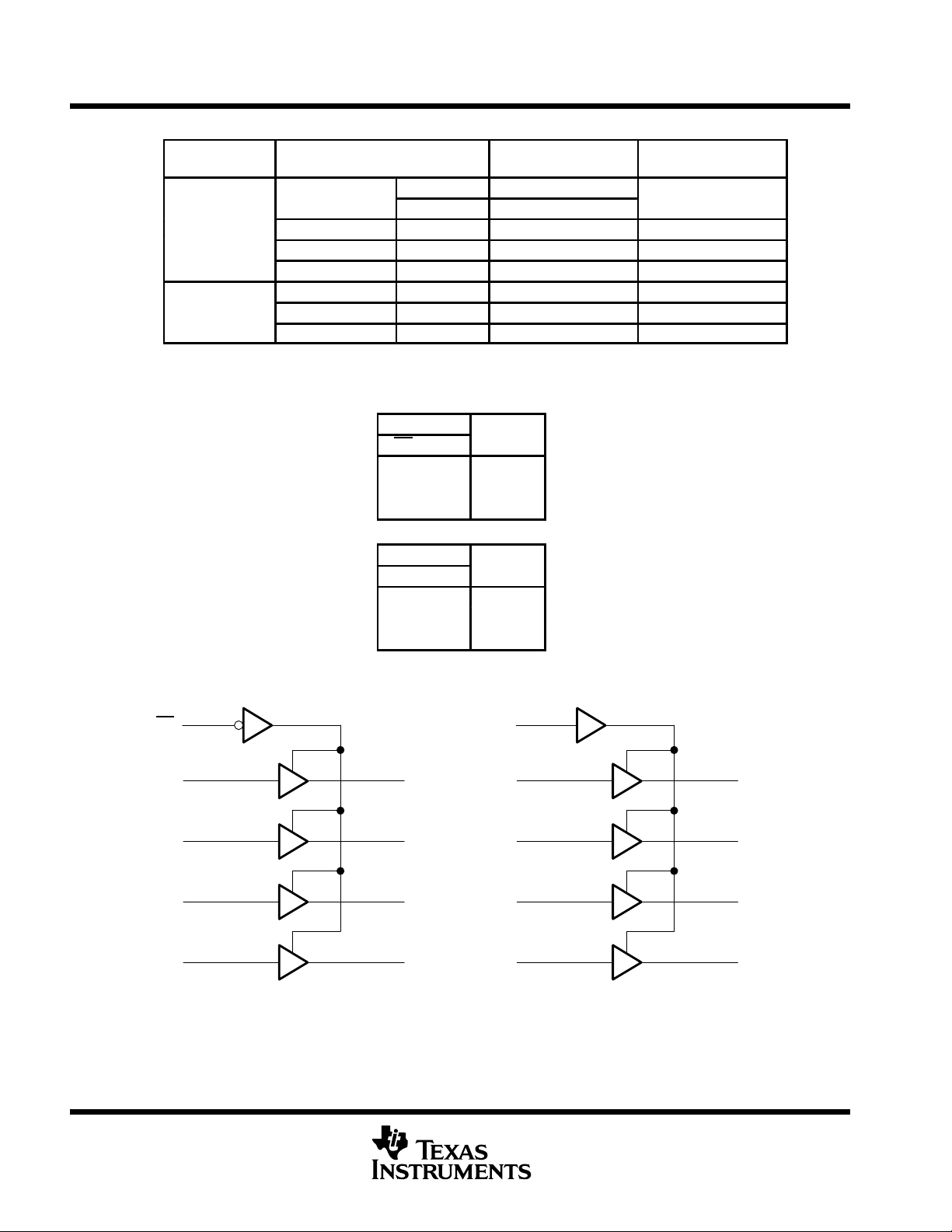
The ’L VTH241 devices are organized as two 4-bit
line drivers with separate output-enable (1OE
2OE) inputs. When 1OE
is low or 2OE is high, the
devices pass noninverted data from the A inputs
to the Y outputs. When 1OE
is high or 2OE is low,
the outputs are in the high-impedance state.
CC
)
CC
operation,
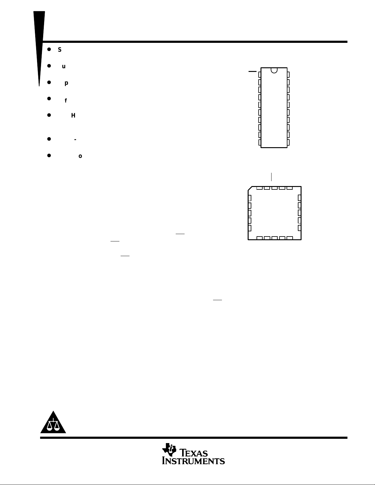
SN54LVTH241...J OR W PACKAGE
SN74LVTH241. . . DB, DW, NS, OR PW PACKAGE
SN54LVTH241. . . FK PACKAGE
1A2
2Y3
1A3
2Y2
1A4
,
1OE
1A1
2Y4
1A2
2Y3
1A3
2Y2
1A4
2Y1
GND
4
5
6
7
8
9 10 11 12 13
(TOP VIEW)
20
1
19
2
18
3
17
4
16
5
15
6
14
7
13
8
12
9
11
10
(TOP VIEW)
1A1
GND
1OE
V
2A1
CC
1Y4
2Y4
3 2 1 20 19
2Y1
V
CC
2OE
1Y1
2A4
1Y2
2A3
1Y3
2A2
1Y4
2A1
2OE
18
17
16
15
14
2A2
1Y1
2A4
1Y2
2A3
1Y3
Active bus-hold circuitry holds unused or undriven inputs at a valid logic state. Use of pullup or pulldown resistors
with the bus-hold circuitry is not recommended.
When V
However, to ensure the high-impedance state above 1.5 V, OE
is between 0 and 1.5 V , the devices are in the high-impedance state during power up or power down.
CC
should be tied to VCC through a pullup resistor
and OE should be tied to GND through a pulldown resistor; the minimum value of the resistor is determined by
the current-sinking/current-sourcing capability of the driver.
These devices are fully specified for hot-insertion applications using I
and power-up 3-state. The I
off
disables the outputs, preventing damaging current backflow through the devices when they are powered down.
The power-up 3-state circuitry places the outputs in the high-impedance state during power up and power down,
which prevents driver conflict.
Please be aware that an important notice concerning availability, standard warranty, and use in critical applications of
Texas Instruments semiconductor products and disclaimers thereto appears at the end of this data sheet.
UNLESS OTHERWISE NOTED this document contains PRODUCTION
DATA information current as of publication date. Products conform to
specifications per the terms of Texas Instruments standard warranty.
Production processing does not necessarily include testing of all
parameters.
Copyright 2002, Texas Instruments Incorporated
circuitry
off
POST OFFICE BOX 655303 • DALLAS, TEXAS 75265
1
Page 2
SN54LVTH241, SN74LVTH241
SOIC
DW
LVTH241
3.3-V ABT OCTAL BUFFERS/DRIVERS
WITH 3-STATE OUTPUTS
SCAS352J – MARCH 1994 – REVISED MARCH 2002
ORDERING INFORMATION
T
A
–40°C to 85°C
–55°C to 125°C
†
Package drawings, standard packing quantities, thermal data, symbolization, and PCB design guidelines are
available at www.ti.com/sc/package.
SOP – NS Tape and reel SN74LVTH241NSR LVTH241
SSOP – DB Tape and reel SN74LVTH241DBR LXH241
TSSOP – PW Tape and reel SN74LVTH241PWR LXH241
CDIP – J Tube SNJ54LVTH241J SNJ54LVTH241J
CFP – W Tube SNJ54LVTH241W SNJ54LVTH241W
LCCC – FK Tube SNJ54LVTH241FK SNJ54LVTH241FK
PACKAGE
–
†
Tube SN74LVTH241DW
Tape and reel SN74LVTH241DWR
FUNCTION TABLES
INPUTS
1OE 1A
L H H
L LL
H X Z
ORDERABLE
PART NUMBER
OUTPUT
1Y
TOP-SIDE MARKING
logic diagram (positive logic)
1
1OE
218
1A1
416
1A2
614
1A3
812
1A4
INPUTS
2OE 2A
H H H
H LL
L X Z
1Y1
1Y2
1Y3
1Y4
OUTPUT
2Y
2OE
2A1
2A2
2A3
2A4
19
11 9
13 7
15 5
17 3
2Y1
2Y2
2Y3
2Y4
2
POST OFFICE BOX 655303 • DALLAS, TEXAS 75265
Page 3
UNIT
SN54LVTH241, SN74LVTH241
3.3-V ABT OCTAL BUFFERS/DRIVERS
WITH 3-STATE OUTPUTS
SCAS352J – MARCH 1994 – REVISED MARCH 2002
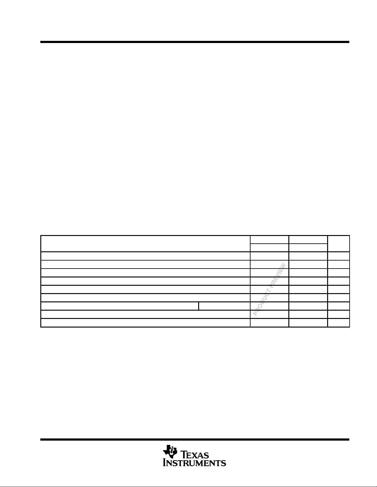
absolute maximum ratings over operating free-air temperature range (unless otherwise noted)
Supply voltage range, V
Input voltage range, V
Voltage range applied to any output in the high-impedance
or power-off state, V
Voltage range applied to any output in the high state, V
Current into any output in the low state, I
Current into any output in the high state, I
Input clamp current, I
Output clamp current, I
Package thermal impedance, θ
Storage temperature range, T
†
Stresses beyond those listed under “absolute maximum ratings” may cause permanent damage to the device. These are stress ratings only, and
functional operation of the device at these or any other conditions beyond those indicated under “recommended operating conditions” is not
implied. Exposure to absolute-maximum-rated conditions for extended periods may affect device reliability.
NOTES: 1. The input and output negative-voltage ratings may be exceeded if the input and output clamp-current ratings are observed.
2. This current flows only when the output is in the high state and VO > VCC.
3. The package thermal impedance is calculated in accordance with JESD 51-7.
–0.5 V to 4.6 V. . . . . . . . . . . . . . . . . . . . . . . . . . . . . . . . . . . . . . . . . . . . . . . . . . . . . . . . .
CC
(see Note 1) –0.5 V to 7 V. . . . . . . . . . . . . . . . . . . . . . . . . . . . . . . . . . . . . . . . . . . . . . . . . .
I
(see Note 1) –0.5 V to 7 V. . . . . . . . . . . . . . . . . . . . . . . . . . . . . . . . . . . . . . . . . . . . . . . .
O
: SN54LVTH241 96 mA. . . . . . . . . . . . . . . . . . . . . . . . . . . . . . . . . . .
O
(see Note 1) –0.5 V to V
O
SN74LVTH241 128 mA. . . . . . . . . . . . . . . . . . . . . . . . . . . . . . . . . .
(see Note 2): SN54LVTH241 48 mA. . . . . . . . . . . . . . . . . . . . . . .
O
SN74LVTH241 64 mA. . . . . . . . . . . . . . . . . . . . . . .
(V
< 0) –50 mA. . . . . . . . . . . . . . . . . . . . . . . . . . . . . . . . . . . . . . . . . . . . . . . . . . . . . . . . . . .
IK
I
(V
OK
< 0) –50 mA. . . . . . . . . . . . . . . . . . . . . . . . . . . . . . . . . . . . . . . . . . . . . . . . . . . . . . . .
O
(see Note 3): DB package 70°C/W. . . . . . . . . . . . . . . . . . . . . . . . . . . . . . . . .
JA
DW package 58°C/W. . . . . . . . . . . . . . . . . . . . . . . . . . . . . . . . .
NS package 60°C/W. . . . . . . . . . . . . . . . . . . . . . . . . . . . . . . . .
PW package 83°C/W. . . . . . . . . . . . . . . . . . . . . . . . . . . . . . . . .
–65°C to 150°C. . . . . . . . . . . . . . . . . . . . . . . . . . . . . . . . . . . . . . . . . . . . . . . . . . .
stg
CC
+ 0.5 V. . . . . . . . . . . . .
†
recommended operating conditions (see Note 4)
SN54LVTH241 SN74LVTH241
MIN MAX MIN MAX
V
CC
V
IH
V
IL
V
I
I
OH
I
OL
∆t/∆v Input transition rise or fall rate Outputs enabled 10 10 ns/V
∆t/∆V
T
A
NOTE 4: All unused control inputs of the device must be held at VCC or GND to ensure proper device operation. Refer to the TI application report,
Supply voltage 2.7 3.6 2.7 3.6 V
High-level input voltage 2 2 V
Low-level input voltage 0.8 0.8 V
Input voltage 5.5 5.5 V
High-level output current –24 –32 mA
Low-level output current 48 64 mA
Power-up ramp rate 200 200 µs/V
CC
Operating free-air temperature –55 125 –40 85 °C
Implications of Slow or Floating CMOS Inputs, literature number SCBA004.
PRODUCT PREVIEW information concerns products in the formative or
design phase of development. Characteristic data and other
specifications are design goals. Texas Instruments reserves the right to
change or discontinue these products without notice.
POST OFFICE BOX 655303 • DALLAS, TEXAS 75265
3
Page 4
SN54LVTH241, SN74LVTH241
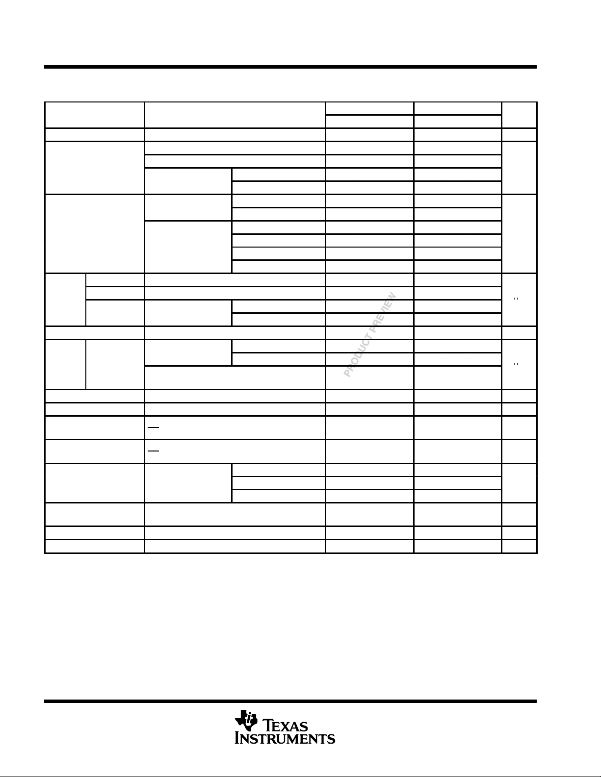
PARAMETER
TEST CONDITIONS
UNIT
V
V
V
3 V
V
2.7 V
V
V
V
3 V
I
A
Data inputs
V
3.6 V
V
3 V
I
I(h
ld)
Data in uts
µA
V
CC
3.3-V ABT OCTAL BUFFERS/DRIVERS
WITH 3-STATE OUTPUTS
SCAS352J – MARCH 1994 – REVISED MARCH 2002
electrical characteristics over recommended operating free-air temperature range (unless
otherwise noted)
SN54LVTH241 SN74LVTH241
MIN TYP†MAX MIN TYP†MAX
V
IK
OH
OL
I
I
off
I
OZH
I
OZL
I
OZPU
I
OZPD
I
CC
∆I
CC
C
i
C
o
∗ On products compliant to MIL-PRF-38535, this parameter is not production tested.
†
All typical values are at VCC = 3.3 V, TA = 25°C.
‡
This is the bus-hold maximum dynamic current. It is the minimum overdrive current required to switch the input from one state to another.
§
This is the increase in supply current for each input that is at the specified TTL voltage level rather than VCC or GND.
Control inputs VCC = 3.6 V, VI = VCC or GND ±1 ±1
p
o
§
p
VCC = 2.7 V, II = –18 mA –1.2 –1.2 V
VCC = 2.7 V to 3.6 V, IOH = –100 µA VCC–0.2 VCC–0.2
VCC = 2.7 V, IOH = –8 mA 2.4 2.4
=
CC
=
CC
=
CC
VCC = 0 or 3.6 V, VI = 5.5 V 10 10
=
CC
VCC = 0, VI or VO = 0 to 4.5 V ±100 µA
=
CC
VCC = 3.6 V‡, VI = 0 to 3.6 V
VCC = 3.6 V, VO = 3 V 5 5 µA
VCC = 3.6 V, VO = 0.5 V –5 –5 µA
VCC = 0 to 1.5 V, VO = 0.5 V to 3 V,
OE
/OE = don’t care
VCC = 1.5 V to 0, VO = 0.5 V to 3 V,
OE
/OE = don’t care
=
= 3.6 V,
IO = 0,
VI = VCC or GND
VCC = 3 V to 3.6 V, One input at VCC – 0.6 V,
Other inputs at VCC or GND
VI = 3 V or 0 3 3 pF
VO = 3 V or 0 7 7 pF
IOH = –24 mA 2
IOH = –32 mA 2
IOL = 100 µA 0.2 0.2
IOL = 24 mA 0.5 0.5
IOL = 16 mA 0.4 0.4
IOL = 32 mA 0.5 0.5
IOL = 48 mA 0.55
IOL = 64 mA 0.55
VI = V
CC
VI = 0 –5 –5
VI = 0.8 V 75 75
VI = 2 V –75 –75
Outputs high 0.19 0.19
Outputs low 5 5
Outputs disabled 0.19 0.19
1 1
500
–750
∗
±100
∗
±100
0.2 0.2 mA
±100 µA
±100 µA
µ
mA
PRODUCT PREVIEW information concerns products in the formative or
design phase of development. Characteristic data and other
specifications are design goals. Texas Instruments reserves the right to
change or discontinue these products without notice.
4
POST OFFICE BOX 655303 • DALLAS, TEXAS 75265
Page 5

A
Y
ns
OE
OE
Y
ns
OE
OE
Y
ns
SN54LVTH241, SN74LVTH241
3.3-V ABT OCTAL BUFFERS/DRIVERS
WITH 3-STATE OUTPUTS
SCAS352J – MARCH 1994 – REVISED MARCH 2002
switching characteristics over recommended ranges of supply voltage and operating free-air
temperature range, C
PARAMETER
t
PLH
t
PHL
t
PZH
t
PZL
t
PHZ
t
PLZ
†
All typical values are at VCC = 3.3 V, TA = 25°C.
(INPUT)
= 50 pF (unless otherwise noted) (see Figure 1)
L
SN54LVTH241 SN74LVTH241
FROM
or
or
TO
(OUTPUT)
VCC = 3.3 V
± 0.3 V
MIN MAX MIN MAX MIN TYP†MAX MIN MAX
1 3.7 4 1.1 2.3 3.5 3.9
1.2 3.5 3.7 1.3 2.2 3.4 3.6
1 4.6 5.5 1.1 2.7 4.5 5.4
1.3 4.6 5.1 1.4 2.9 4.4 5
1.5 4.7 5.5 1.6 2.8 4.5 5.3
1.7 5 5.5 1.8 3 4.7 5.2
VCC = 2.7 V
VCC = 3.3 V
± 0.3 V
VCC = 2.7 V
UNIT
PRODUCT PREVIEW information concerns products in the formative or
design phase of development. Characteristic data and other
specifications are design goals. Texas Instruments reserves the right to
change or discontinue these products without notice.
POST OFFICE BOX 655303 • DALLAS, TEXAS 75265
5
Page 6

SN54LVTH241, SN74LVTH241
3.3-V ABT OCTAL BUFFERS/DRIVERS
WITH 3-STATE OUTPUTS
SCAS352J – MARCH 1994 – REVISED MARCH 2002
PARAMETER MEASUREMENT INFORMATION
6 V
From Output
Under Test
CL = 50 pF
(see Note A)
500 Ω
500 Ω
S1
GND
Open
TEST S1
t
PLH/tPHL
t
PLZ/tPZL
t
PHZ/tPZH
Open
6 V
GND
LOAD CIRCUIT
t
w
Input
Input
Output
Output
INVERTING AND NONINVERTING OUTPUTS
NOTES: A. CL includes probe and jig capacitance.
B. Waveform 1 is for an output with internal conditions such that the output is low except when disabled by the output control.
C. All input pulses are supplied by generators having the following characteristics: PRR ≤ 10 MHz, ZO = 50 Ω, tr ≤ 2.5 ns , tf≤ 2.5 ns.
D. The outputs are measured one at a time with one transition per measurement.
1.5 V
VOLTAGE WAVEFORMS
PULSE DURATION
1.5 V 1.5 V
t
PLH
1.5 V
t
PHL
VOLTAGE WAVEFORMS
PROPAGATION DELAY TIMES
Waveform 2 is for an output with internal conditions such that the output is high except when disabled by the output control.
1.5 V
1.5 V
1.5 V1.5 V
t
PHL
t
PLH
2.7 V
0 V
2.7 V
0 V
V
OH
V
OL
V
OH
V
OL
Timing Input
Data Input
Output
Control
Output
Waveform 1
S1 at 6 V
(see Note B)
Output
Waveform 2
S1 at GND
(see Note B)
1.5 V
t
su
1.5 V 1.5 V
VOLTAGE WAVEFORMS
SETUP AND HOLD TIMES
t
PZL
1.5 V
t
PZH
1.5 V
VOLTAGE WAVEFORMS
ENABLE AND DISABLE TIMES
LOW- AND HIGH-LEVEL ENABLING
t
h
1.5 V1.5 V
t
VOL + 0.3 V
t
VOH – 0.3 V
PLZ
PHZ
2.7 V
0 V
2.7 V
0 V
2.7 V
0 V
3 V
V
OL
V
OH
≈0 V
Figure 1. Load Circuit and Voltage Waveforms
6
POST OFFICE BOX 655303 • DALLAS, TEXAS 75265
Page 7

MECHANICAL DATA
MSOI003E – JANUARY 1995 – REVISED SEPTEMBER 2001
DW (R-PDSO-G**) PLASTIC SMALL-OUTLINE PACKAGE
16 PINS SHOWN
0.050 (1,27)
16
1
0.020 (0,51)
0.014 (0,35)
9
0.299 (7,59)
0.291 (7,39)
8
A
0.010 (0,25)
0.419 (10,65)
0.400 (10,15)
Seating Plane
0.010 (0,25) NOM
Gage Plane
0°– 8°
0.010 (0,25)
0.050 (1,27)
0.016 (0,40)
0.104 (2,65) MAX
NOTES: A. All linear dimensions are in inches (millimeters).
B. This drawing is subject to change without notice.
C. Body dimensions do not include mold flash or protrusion not to exceed 0.006 (0,15).
D. Falls within JEDEC MS-013
0.012 (0,30)
0.004 (0,10)
PINS **
DIM
A MAX
A MIN
0.004 (0,10)
16
0.410 0.462
(10,41)
0.400
(10,16)
18
(11,73)
0.453
(11,51)
20
0.510
(12,95)
0.500
24
0.610
(15,49)
0.600
(15,24)
28
0.710
(18,03)
0.700
(17,78)(12,70)
4040000/E 08/01
POST OFFICE BOX 655303 • DALLAS, TEXAS 75265
1
Page 8

MECHANICAL DATA
MSOP002 – OCTOBER 1994
NS (R-PDSO-G**) PLASTIC SMALL-OUTLINE PACKAGE
14 PINS SHOWN
1,27
14
1
2,00 MAX
0,51
0,35
8
5,60
5,00
7
A
0,05 MIN
M
0,25
8,20
7,40
Seating Plane
0,10
0,15 NOM
Gage Plane
0°–10°
0,25
1,05
0,55
DIM
A MAX
NOTES: A. All linear dimensions are in millimeters.
B. This drawing is subject to change without notice.
C. Body dimensions do not include mold flash or protrusion, not to exceed 0,15.
PINS **
A MIN
16
10,501410,50
9,90 9,90
20 24
15,3012,90
12,30 14,70
4040062/B 02/95
POST OFFICE BOX 655303 • DALLAS, TEXAS 75265
1
Page 9

MECHANICAL DATA
MSSO002E – JANUARY 1995 – REVISED DECEMBER 2001
DB (R-PDSO-G**) PLASTIC SMALL-OUTLINE
28 PINS SHOWN
0,65
28
1
2,00 MAX
0,38
0,22
15
14
A
0,05 MIN
0,15
5,60
5,00
M
8,20
7,40
Seating Plane
0,10
0,25
0,09
0°–ā8°
Gage Plane
0,25
0,95
0,55
PINS **
DIM
A MAX
A MIN
NOTES: A. All linear dimensions are in millimeters.
B. This drawing is subject to change without notice.
C. Body dimensions do not include mold flash or protrusion not to exceed 0,15.
D. Falls within JEDEC MO-150
14
6,50
6,50
5,905,90
2016
7,50
6,90
24
8,50
28
10,50
9,907,90
30
10,50
9,90
38
12,90
12,30
4040065 /E 12/01
POST OFFICE BOX 655303 • DALLAS, TEXAS 75265
1
Page 10

MECHANICAL DATA
MTSS001C – JANUARY 1995 – REVISED FEBRUARY 1999
PW (R-PDSO-G**) PLASTIC SMALL-OUTLINE PACKAGE
14 PINS SHOWN
0,65
1,20 MAX
14
0,30
0,19
8
4,50
4,30
PINS **
7
Seating Plane
0,15
0,05
8
1
A
DIM
14
0,10
6,60
6,20
M
0,10
0,15 NOM
0°–8°
2016
Gage Plane
24
0,25
0,75
0,50
28
A MAX
A MIN
NOTES: A. All linear dimensions are in millimeters.
B. This drawing is subject to change without notice.
C. Body dimensions do not include mold flash or protrusion not to exceed 0,15.
D. Falls within JEDEC MO-153
3,10
2,90
5,10
4,90
5,10
4,90
6,60
6,40
7,90
7,70
9,80
9,60
4040064/F 01/97
POST OFFICE BOX 655303 • DALLAS, TEXAS 75265
1
Page 11

IMPORTANT NOTICE
Texas Instruments Incorporated and its subsidiaries (TI) reserve the right to make corrections, modifications,
enhancements, improvements, and other changes to its products and services at any time and to discontinue
any product or service without notice. Customers should obtain the latest relevant information before placing
orders and should verify that such information is current and complete. All products are sold subject to TI’s terms
and conditions of sale supplied at the time of order acknowledgment.
TI warrants performance of its hardware products to the specifications applicable at the time of sale in
accordance with TI’s standard warranty . Testing and other quality control techniques are used to the extent TI
deems necessary to support this warranty . Except where mandated by government requirements, testing of all
parameters of each product is not necessarily performed.
TI assumes no liability for applications assistance or customer product design. Customers are responsible for
their products and applications using TI components. T o minimize the risks associated with customer products
and applications, customers should provide adequate design and operating safeguards.
TI does not warrant or represent that any license, either express or implied, is granted under any TI patent right,
copyright, mask work right, or other TI intellectual property right relating to any combination, machine, or process
in which TI products or services are used. Information published by TI regarding third–party products or services
does not constitute a license from TI to use such products or services or a warranty or endorsement thereof.
Use of such information may require a license from a third party under the patents or other intellectual property
of the third party , or a license from TI under the patents or other intellectual property of TI.
Reproduction of information in TI data books or data sheets is permissible only if reproduction is without
alteration and is accompanied by all associated warranties, conditions, limitations, and notices. Reproduction
of this information with alteration is an unfair and deceptive business practice. TI is not responsible or liable for
such altered documentation.
Resale of TI products or services with statements different from or beyond the parameters stated by TI for that
product or service voids all express and any implied warranties for the associated TI product or service and
is an unfair and deceptive business practice. TI is not responsible or liable for any such statements.
Mailing Address:
Texas Instruments
Post Office Box 655303
Dallas, Texas 75265
Copyright 2002, Texas Instruments Incorporated
 Loading...