

Page 1
SNC745
1
16-bit Voice Processor
1. INTRODUCTION
SNC745 is a 64mins two-channel speech/melody and 4-channel wave-table melody
voice chip. It based on reduced 16-bit fixed-point DSP architecture. SNC745 provides
user some necessary and efficient DSP instructions. Furthermore, SNC745 provide one
10-bit PWM and one 10-bit DA converter to driving speaker for speech/melody output.
User can select PWM or DA by programming DA/PWM control register, and only one
function can be active at the same time.
2. FEATURES
w Power supply: 2.4V ~ 3.6V (for 2 battery application)
3.6V ~ 5.1V (for 3 battery application)
w Built-in a 16-bit DSP (Very Light Structure)
w Software-based voice/melody processing
w Rich Function Instruction Set
w System Clock
− 16MHz crystal or R-C type oscillator for system clock
− 0.25s real time clock is form 32768Hz crystal
w 8 MI PS CPU performance
w I/O Ports:
− 16 I/O pins (P0.0~P0.15) and 8 input pins (P1.0~P1.7)
− P0.15 with IR carrier signal
w RAM size: 2K*16 bits
w High performance program ROM: 32K*16 bits
w Data ROM size: 480K*16 bits
w Total ROM size: 512K*16 bits
w Maximum program size: 64K word
w 8 Interrupt Sources
− 4 for Internal Timer (timer0, 1, 2 and RTC)
− 4 for External (P0.0~P0.3)
w Two voice/melody channels
w Three 8-bit timer with auto-reload function
w Built in a 10-bit PWM Direct Drive circuit and a fixed current D/A output
w Sampling Rate: 6KHz ~16KHz
w Built-in software voice synthesizer (multiple bit -rate solution 2Kbps, 3.6Kbps, 5Kbps,
6Kbps, 8Kbps, 10Kbps, 12Kbps, 14Kbps, 16Kbps, 20Kbps, 24Kbps and 29Kbps
@8K sampling rate)
w Built-in software melody synthesizer includes the dual -tone melody and 4-ch
wave-table melody.
w Low Voltage Reset
Ver. 1.3 October 23, 2002
Page 2
2
3. PIN ASSIGNMENT
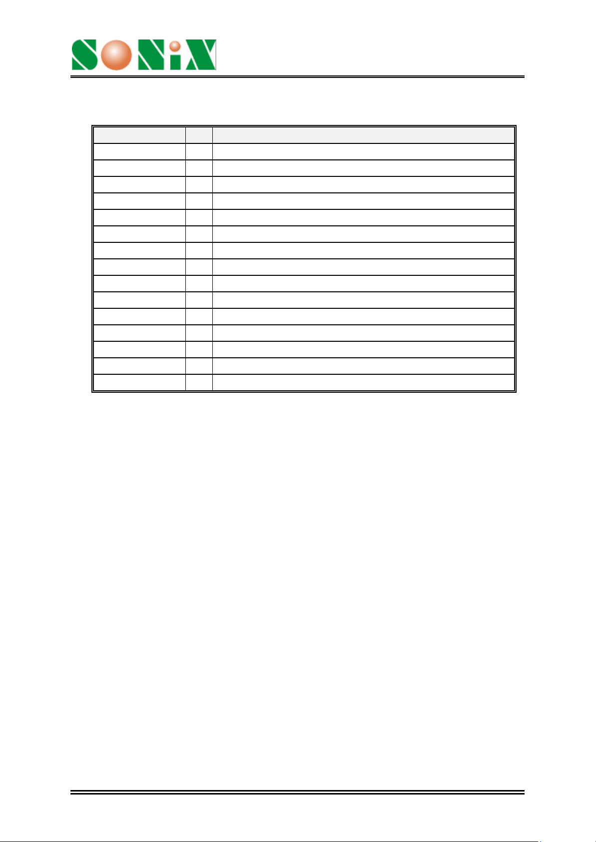
Symbol I/O Descriptions
P0.0 ~ P0.15 I/O I/O port 0
P1.0 ~ P1.7 I Input port 1
CVDD I Positive power supply for core circuit
VDD I Positive power suppl y
GND I Negative power supply
BP0 O PWM output 1
BN0 O PWM output 2
VO O DA output
XIN I High speed clock crystal input / RC-type oscillator input
XOUT O High speed clock crystal output / RC-type oscillator input
LXIN I Low speed clock crystal input
LXOUT O Low speed clock crystal output
CKSEL I Crystal/RC-type oscillator select for high speed clock
RST I Chip reset
TEST I For test only
SNC745
16-bit Voice Processor
Ver. 1.3 October 23, 2002
Page 3
SNC745
3
16-bit Voice Processor
4. ROM TABLE
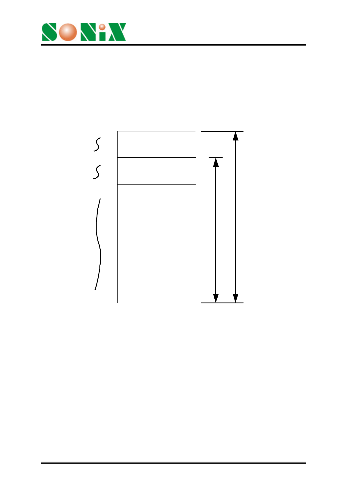
The total ROM size is 512K words. But only 64K words ROM for programming.
And 32K words of all is the high speed program ROM. The high -low speed ratio is 1:16,
that is to say, if the instruction cycle is two clocks at high speed ROM, the instruction cycle
will down to 32 clocks at low speed ROM.
0x000000
Hi-Speed ROM
(32K words)
0x007FFF
0x008000
0x00FFFF
0x010000
Low-Speed program
ROM
(32K words)
Low-Speed Data ROM (480K words)
Total ROM size (512K words)
0x07FFFF
Data ROM
Ver. 1.3 October 23, 2002
Page 4
SNC745
4
16-bit Voice Processor
5. RAM TABLE
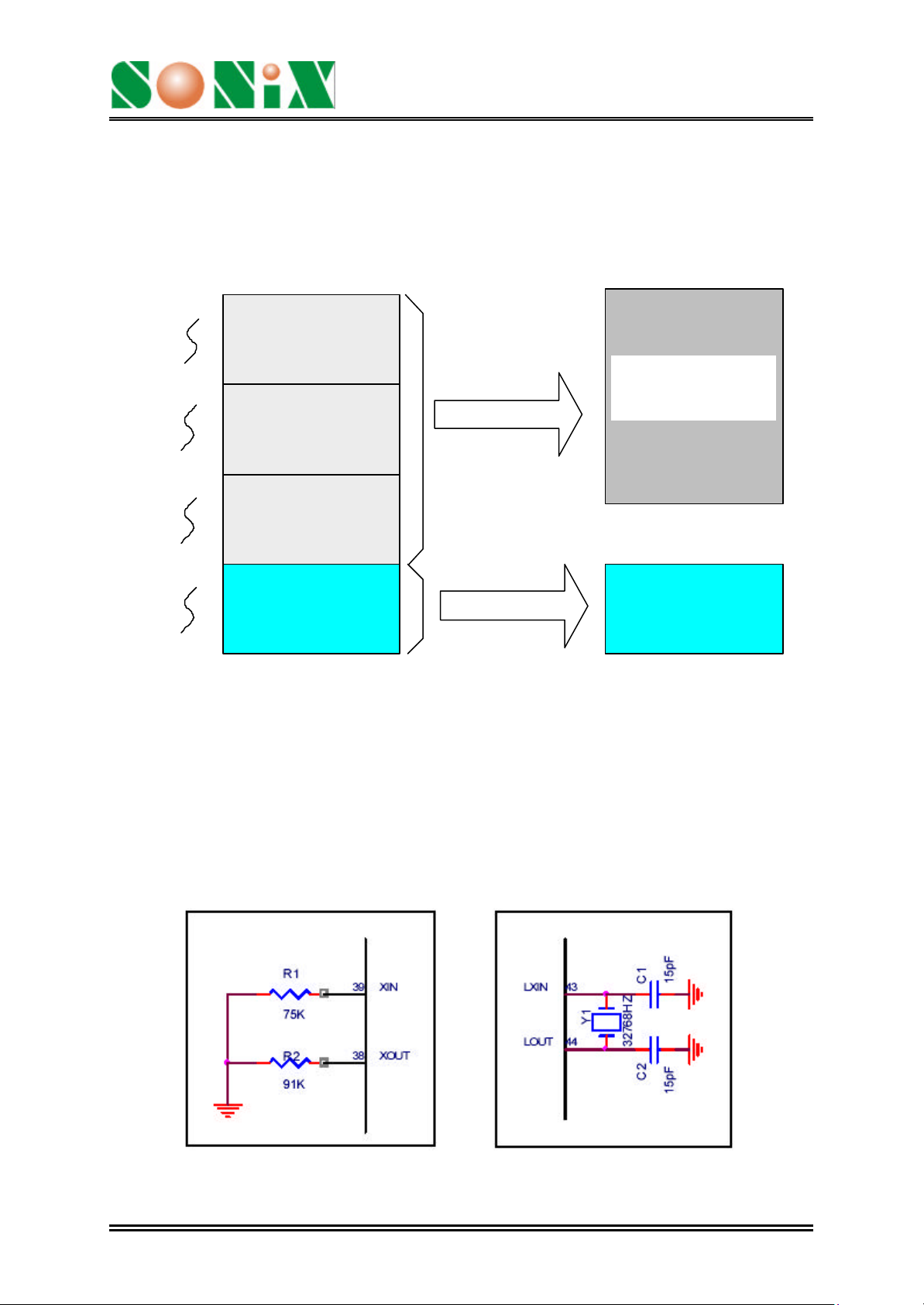
Total RAM size is 2K words, and one bank is 512 words. If user need playing voice
(2Kbps, 3.6Kbps, 12Kbps, dual-tone melody and 4-ch wave -table melody), the system
will reserve 1.5K words RAM size.
0x0000
Bank0
0x01FF
0x0200
Bank1
0x03FF
0x0400
Bank2
0x05FF
0x0600
Bank3 Free for User
0x07FF
Reserved for
OS and Voice
Algorithm
6. System Clock
The system clock source also can be selected from 16Mhz crystal or ROSC. For the
ROSC, user should connect two resistors in the pin “XIN” and “XOUT” instead of 16MHZ
crystal. Beside, the clock source select pin “CKSEL” also should be connected to VDD
for ROSC. In order to get an accurate system clock by ROSC, the real time clock
source is recommended to connect a 32768HZ crystal for system clock
calibration.
Ver. 1.3 October 23, 2002
Page 5
SNC745
5
Input Control
16-bit Voice Processor
7. I/O PORT
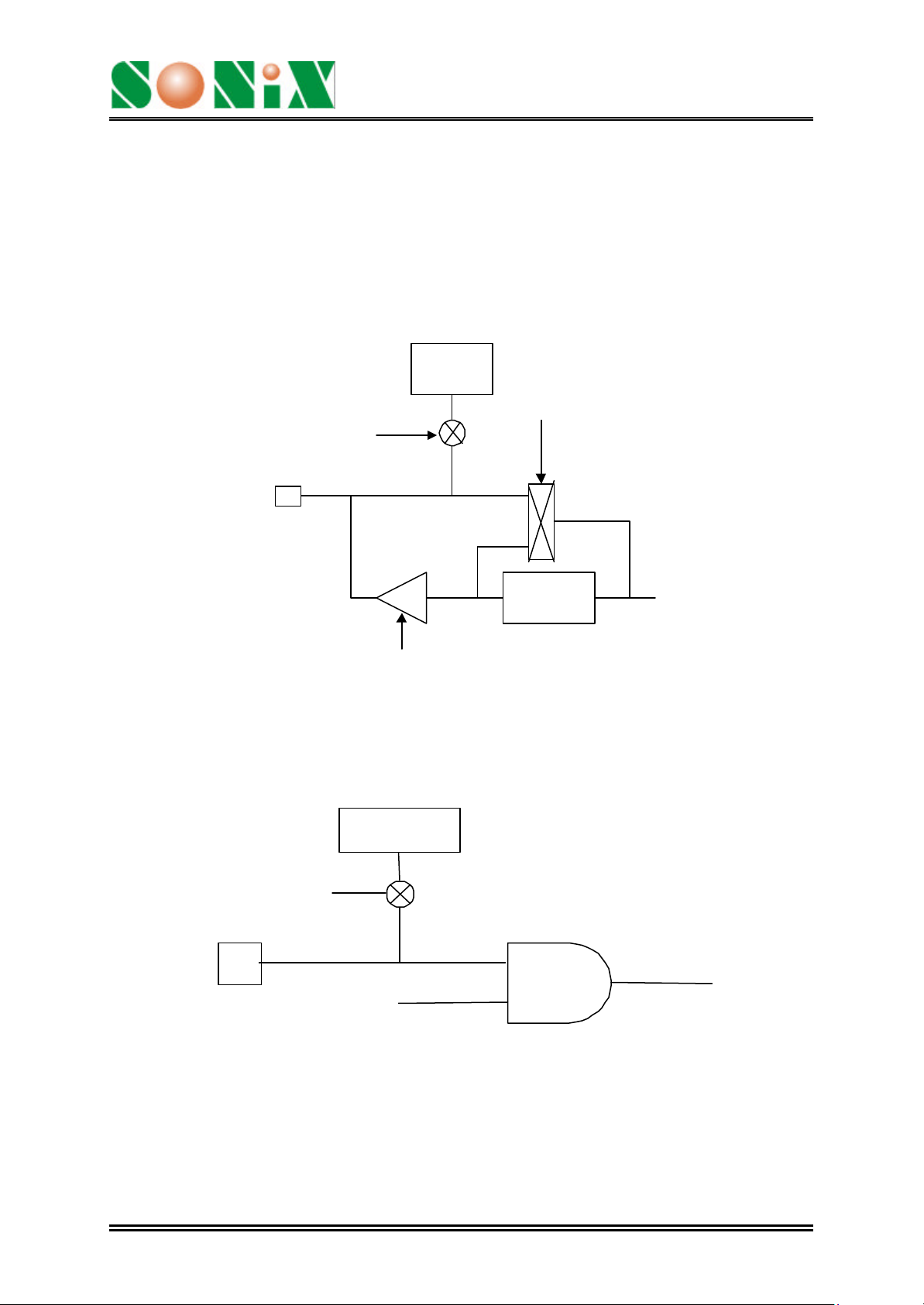
SNC745 provides one a 16-bit I/O port and an 8-bit input port for user application
(P0.0~P0.15, P1.0~P1.7). The input pull high resistor of each pin can be programmed by
Port Pull-High register. The direction of I/O port is selected by Port Direction register. The
Port0 (P0.0~P0.15) and Port1 (P1.0~P1.7) can wake the chip up from the stop mode and
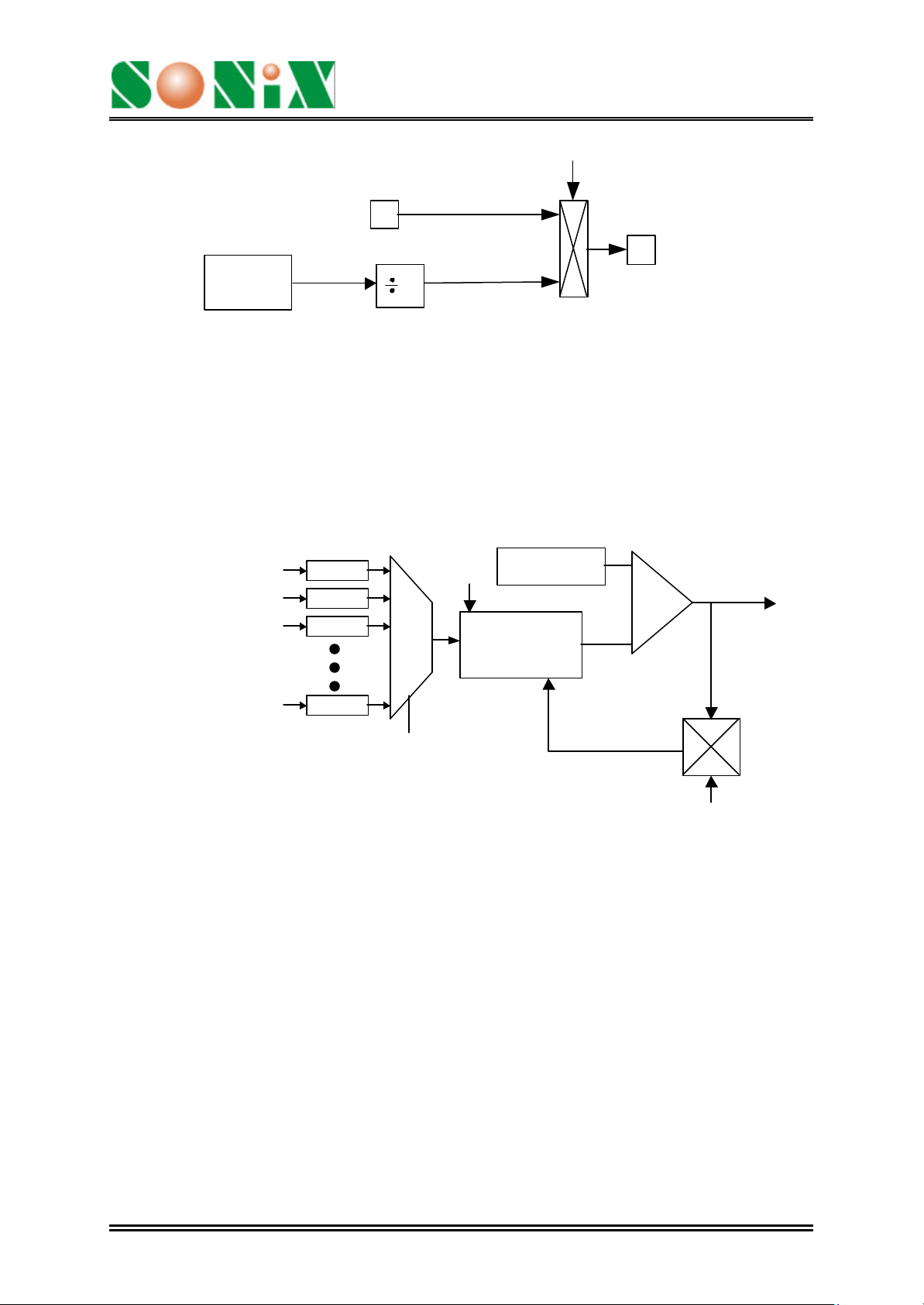
watch mode. P0.15 can be modulated with a 38.5Khz carry signal to realize IR signal
transmission.
Pull-Up
Resister
In/Out
Pull-Up
Select
PAD
Control
Latch
In/Out
Control
to internal bus
I/O Configuration of P0.0~P0.15
Pull-Up
Resister
PAD
Input Port Configuration of Port 1 (P1.0~P1.7)
Ver. 1.3 October 23, 2002
Page 6
SNC745
6
/2
/4
/8
/256
16-bit Voice Processor
IREN
Timer2
P0.15
Overflow
I/O Pad
2
P0.15 Modulated with a carry signal
8. TIMER/COUNTER
SNC745 provides three 8-bit timer/event counters (T0/T1/T2). Each timer is 8-bit binary
up-count timer with pre-scalar and auto-reload function. Timer 0 (T0) is used when voice
playing, so user should avoid to use T0.
Enable
TnC (8-bit)
If equal, Time out
(system clock)/2*
8-bit Up
Counter
clear
comparator
Pre-scalar
Auto-reload
9. DAC & PWM
To play out voices, SNC745 contains two different solutions, DAC and PWM, for the
users’ applications. The user can choose one of these two solutions in his design. Only
one function can be activated at one time.
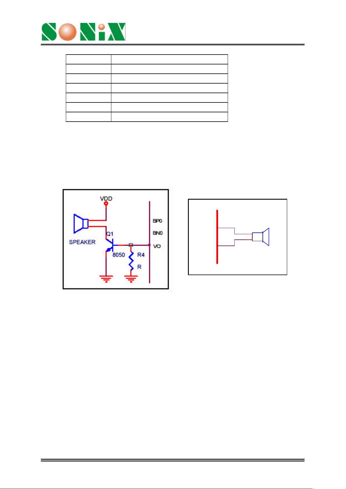
DAC: A 10-bit current type digital-to-analog converter is built-in SNC745. The
relationship between input digital data and output analog current is listed in the following
table. Also, the recommended application circuit is illustrated as follows.
Ver. 1.3 October 23, 2002
Page 7
SNC745
7
16-bit Voice Processor
Input data Typical value of output current (mA)
0 0
1 3/1024
…
N n*(3/1024)
…
1024 3
PWM: A PWM (pulse width modulation) circuit is built-in SNC745. PWM can convert
input digital data into pulse trains with suitable different pulse width. The maximum
resolution of PWM is 10 bits. Two huge output stage circuits are included in SNC745.
Both of them are capable of driving speaker directly. The recommended application
circuit is as follows.
DAC output PWM output
BP0
BN0
SPEAKER
Ver. 1.3 October 23, 2002
Page 8
SNC745
8
16-bit Voice Processor
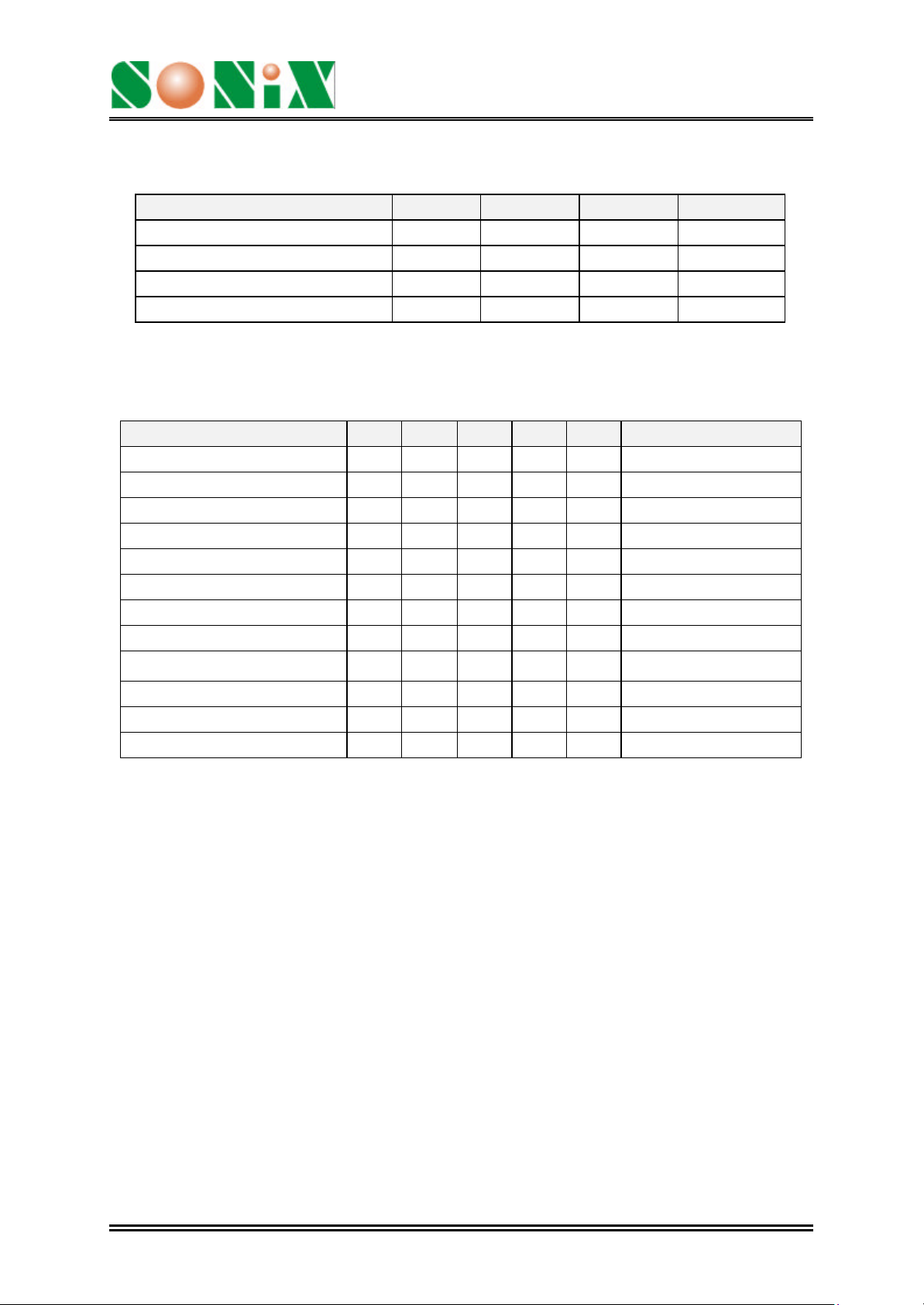
10. ABSOLUTE MAXIMUM RATINGS
Items Symbol Min Max Unit.
Supply Voltage VDD-V -0.3 6.0 V
Input Voltage VIN GND-0.3 VDD+0.3 V
Operating Temperature TOP -20.0 70.0
Storage Temperature T
-55.0 125.0
STG
o
C
o
C
11. ELECTRICAL CHARACTERISTICS
Item Sym. Min. Typ. Max. Unit Condition
Operating Voltage VDD 2.4 - 3.6 V *1.
VDD 3.6 - 5.1 V *2.
Standby current I
Operating Current I
Input current of P0, P1 IIH - - 10.0 uA VDD=3V,VIN=3V
Drive current of P0 IOD - 10 - mA VDD=3V,VO=2.4V
Sink Current of P0 IOS - 12 - mA VDD=3V,VO=0.4V
Drive current of Buo1 IOD 100 120 - mA VDD=3V,Buo1=1.5V
Sink Current of Buo1 IOS 100 120 - mA VDD=3V,Buo1=1.5V
- - 2.0 uA VDD=3V, no load
SBY
- - 5 mA VDD=3V, no load
OPR
Drive Current of Buo2 IOD 100 120 - mA VDD=3V,Buo2=1.5V
Sink Current of Buo2 IOS 100 120 - mA VDD=3V,Buo2=1.5V
Oscillation Freq. (crystal) F
- 16.0 - MHz VDD=3V
OSC
Note:
1. For 2 battery application.
2. For 3 battery application, user should add 1 resister between power and CVDD pin
of chip.
Ver. 1.3 October 23, 2002
Page 9
SNC745
9
Frequency
16-bit Voice Processor
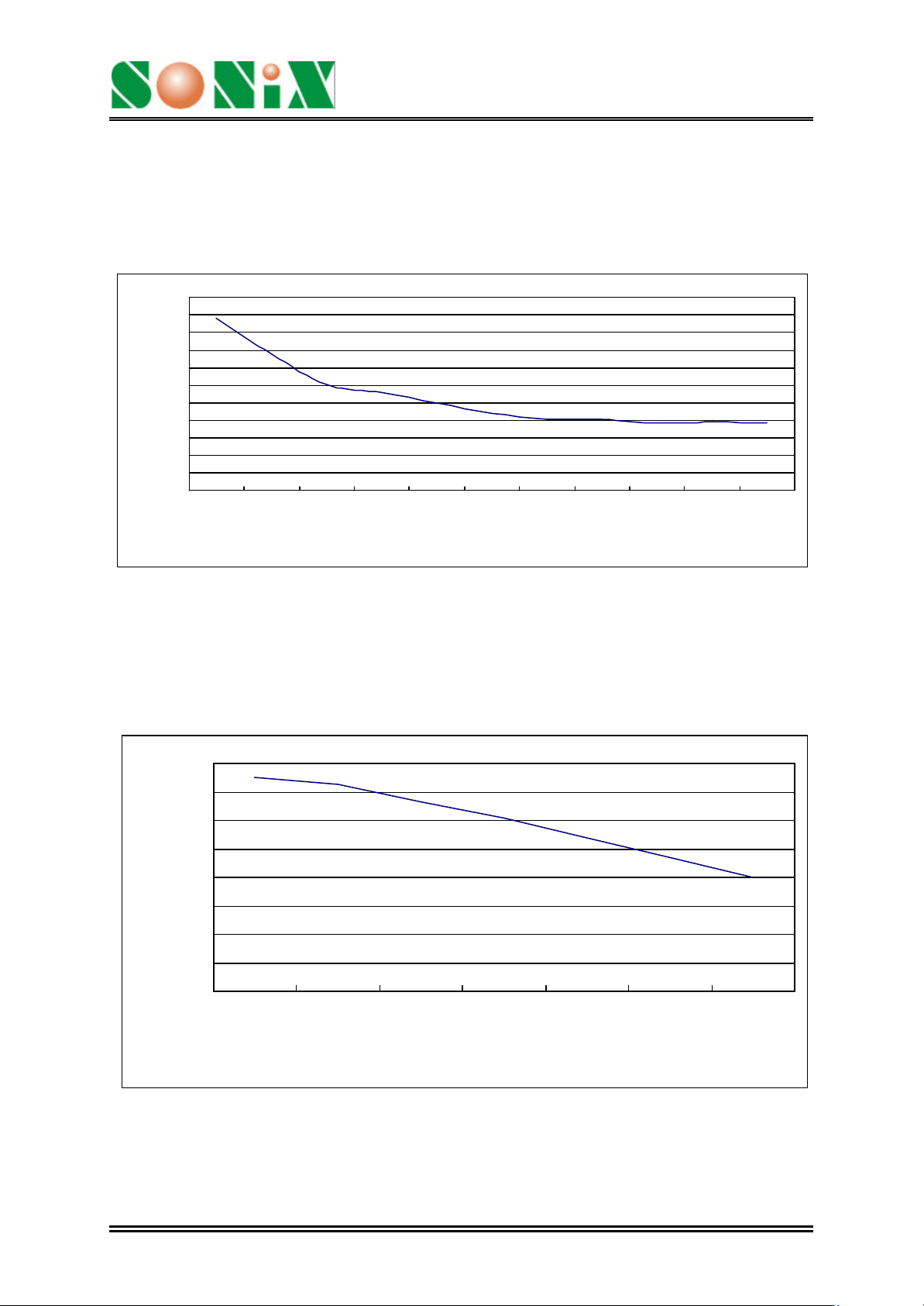
The relationship between ROSC and voltage (Typical)
Ta = 25 °C
Frequency unit: MHz
17.4
17.2
17
16.8
16.6
16.4
16.2
16
15.8
15.6
15.4
15.2
2.0 V
The relationship between Frequency and Resister (R2) for ROSC (Typical)
Ta = 25 °C, R1 = 75KΩ
Frequency unit: MHz
18
17
16
15
14
13
Frequency
12
11
10
2.2 V
2.4 V
2.6 V
2.8 V
3.0 V
Voltage
3.2 V
3.4 V
3.6 V
3.8 V
74K 82K 91K 100K 110K 120K 130K
Resister Value
4.0 V
Ver. 1.3 October 23, 2002
Page 10
16-bit Voice Processor
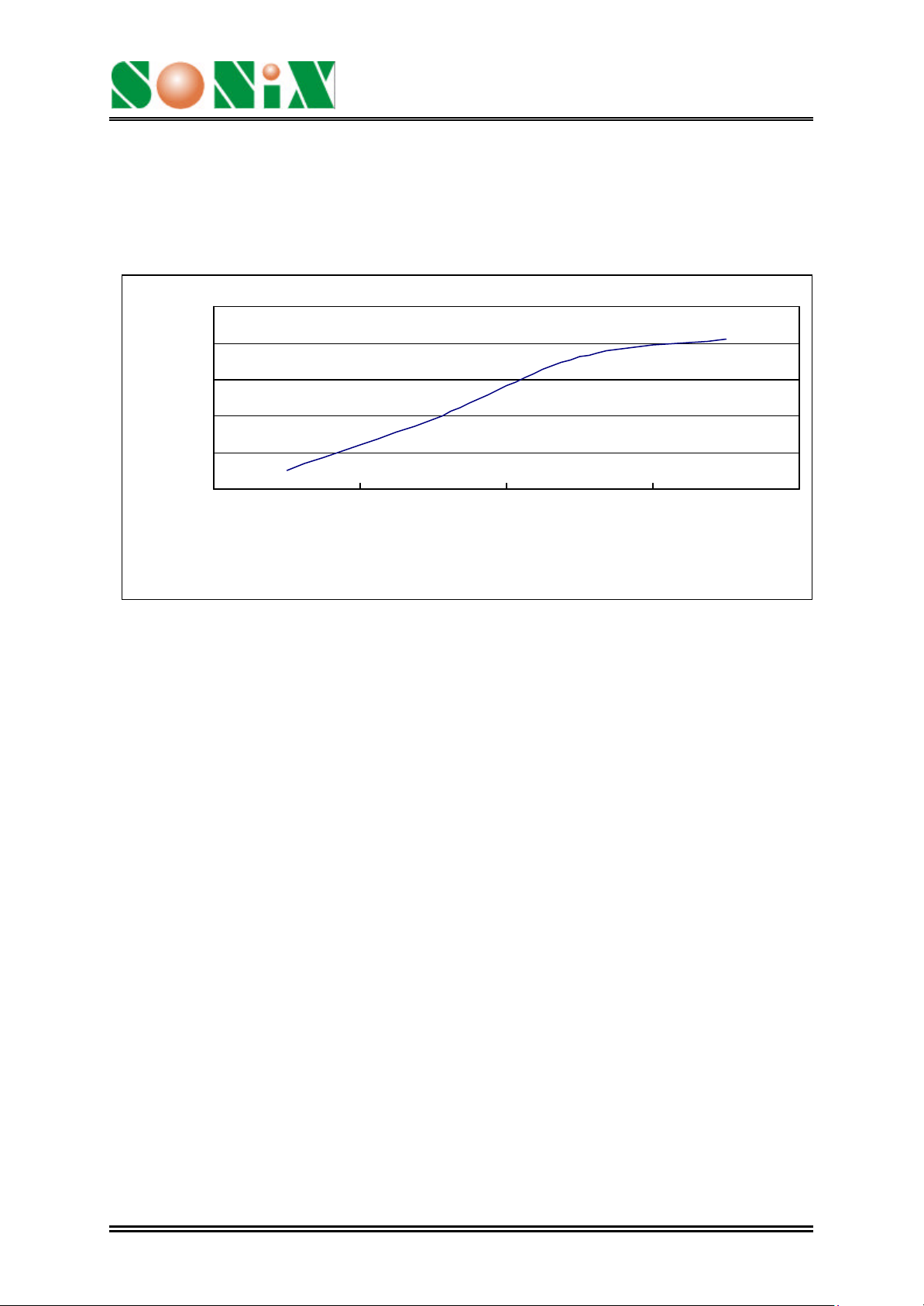
The relationship between operating current and voltage (Typical)
Ta = 25 °C
Current unit: mA
7
6
5
4
Current
3
2
1.8 V 2.4 V 3 V 4.1 V
Voltage
SNC745
Ver. 1.3 October 23, 2002
10
Page 11
SNC745
16-bit Voice Processor
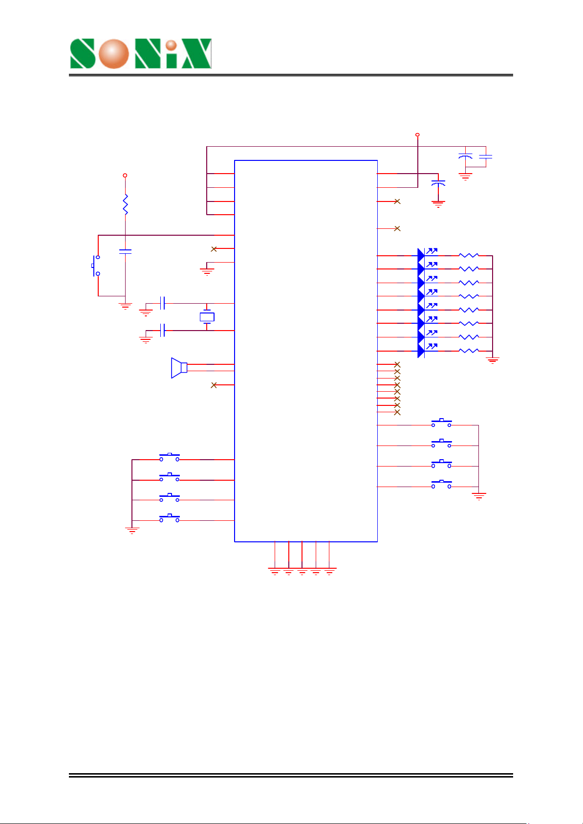
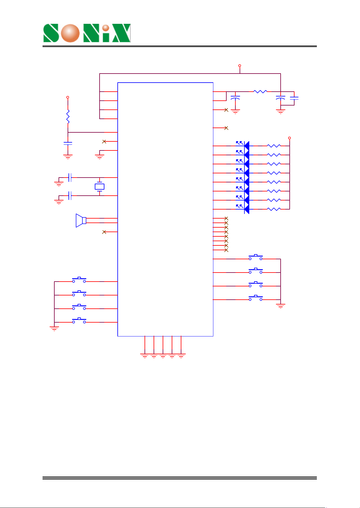
12. APPLICATION CIRCUIT
RESET
VDD
R1
220K
C1
S1
0.1u
SPEAKER
C2 15p
C3 15p
LS1
TR5
TR6
TR7
TR8
Y1
16MHz
U1 SNC745
3
VDD
10
VDD
23
VDD
43
VDD
13
RST
7
TEST
6
CKSEL
40
XIN
39
XOUT
2
BP0
4
BN0
42
VO
35
P1.4
36
P1.5
37
P1.6
38
P1.7
GND1GND5GND14GND32GND
CVDD
CVDD
LXIN
LXOUT
P0.0
P0.1
P0.2
P0.3
P0.4
P0.5
P0.6
P0.7
P0.8
P0.9
P0.10
P0.11
P0.12
P0.13
P0.14
P0.15
P1.0
P1.1
P1.2
P1.3
41
3V, 16MHz Crystal, PWM
Note:
1. All the ”VDD” and “CVDD” should be connected together before connected to the
power source which with a 47uF(C4) capacitor.
2. The capacitor “C5” is near the “CVDD” pin.
VDD (3V)
C4
TR1
TR2
TR3
TR4
47u
C5
4.7u
330
330
330
330
330
330
330
330
15
31
44
45
8
9
11
12
16
17
18
19
20
21
22
24
25
26
27
28
29
30
33
34
C6
0.1u
Ver. 1.3 October 23, 2002
11
Page 12
SNC745
16-bit Voice Processor
VDD (4.5V)
R1
220K
C2 15p
C3 15p
LS1
SPEAKER
C1
0.1u
TR5
TR6
TR7
TR8
Y1
16MHz
U1 SNC745
3
VDD
10
VDD
23
VDD
43
VDD
13
RST
7
TEST
6
CKSEL
40
XIN
39
XOUT
2
BP0
4
BN0
42
VO
35
P1.4
36
P1.5
37
P1.6
38
P1.7
GND1GND5GND14GND32GND
15
CVDD
31
CVDD
44
LXIN
P0.0
P0.1
P0.2
P0.3
P0.4
P0.5
P0.6
P0.7
P0.8
P0.9
P0.10
P0.11
P0.12
P0.13
P0.14
P0.15
P1.0
P1.1
P1.2
P1.3
45
8
9
11
12
16
17
18
19
20
21
22
24
25
26
27
28
29
30
33
34
LXOUT
41
4.5V, 16MHz Crystal, PWM
Note:
1. All the ”VDD” should be connected together before connected to the power source
which with a 47uF(C4) capacitor.
2. The capacitor “C5” is near the “CVDD” pin.
VDD (4.5V)
C5
4.7u
TR1
TR2
TR3
TR4
R2 360
C4
47u
330
330
330
330
330
330
330
330
VDD (4.5V)
C6
0.1u
Ver. 1.3 October 23, 2002
12
Page 13
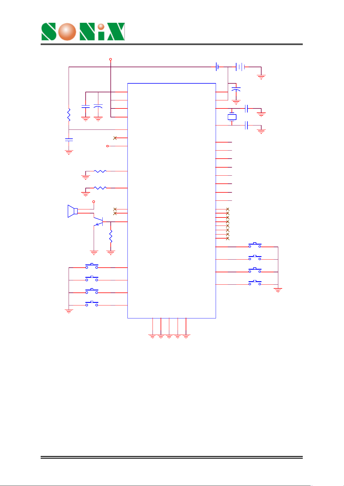
SNC745
16-bit Voice Processor
VDD
BT2
CVDD
CVDD
LXIN
LXOUT
P0.0
P0.1
P0.2
P0.3
P0.4
P0.5
P0.6
P0.7
P0.8
P0.9
P0.10
P0.11
P0.12
P0.13
P0.14
P0.15
P1.0
P1.1
P1.2
P1.3
BATTERY
15
31
44
45
8
9
11
12
16
17
18
19
20
21
22
24
25
26
27
28
29
30
33
34
SPEAKER
R1
220K
LS1
C1
0.1u
C6
0.1u
VDD
TR5
TR6
TR7
TR8
VCC
VR1
75K
VR2
100K
8050
Q1
C4
47u
U1 SNC745
3
VDD
10
VDD
23
VDD
43
VDD
13
RST
7
TEST
6
CKSEL
40
XIN
39
XOUT
2
BP0
4
BN0
42
VO
R7
R
35
P1.4
36
P1.5
37
P1.6
38
P1.7
GND1GND5GND14GND32GND
41
I/O and VDD 4.5V, CVDD 3V, 16MHz ROSC, DA output
Note:
1. All the ”VDD” should be connected together before connected to the power source
which with a 47uF(C4) capacitor.
2. The capacitor “C5” is near the “CVDD” pin.
3V4.5V
BT1
BATTERY
C5
4.7u
C7
15p
Y1
32768
C8 15p
TR1
TR2
TR3
TR4
Ver. 1.3 October 23, 2002
13
Page 14
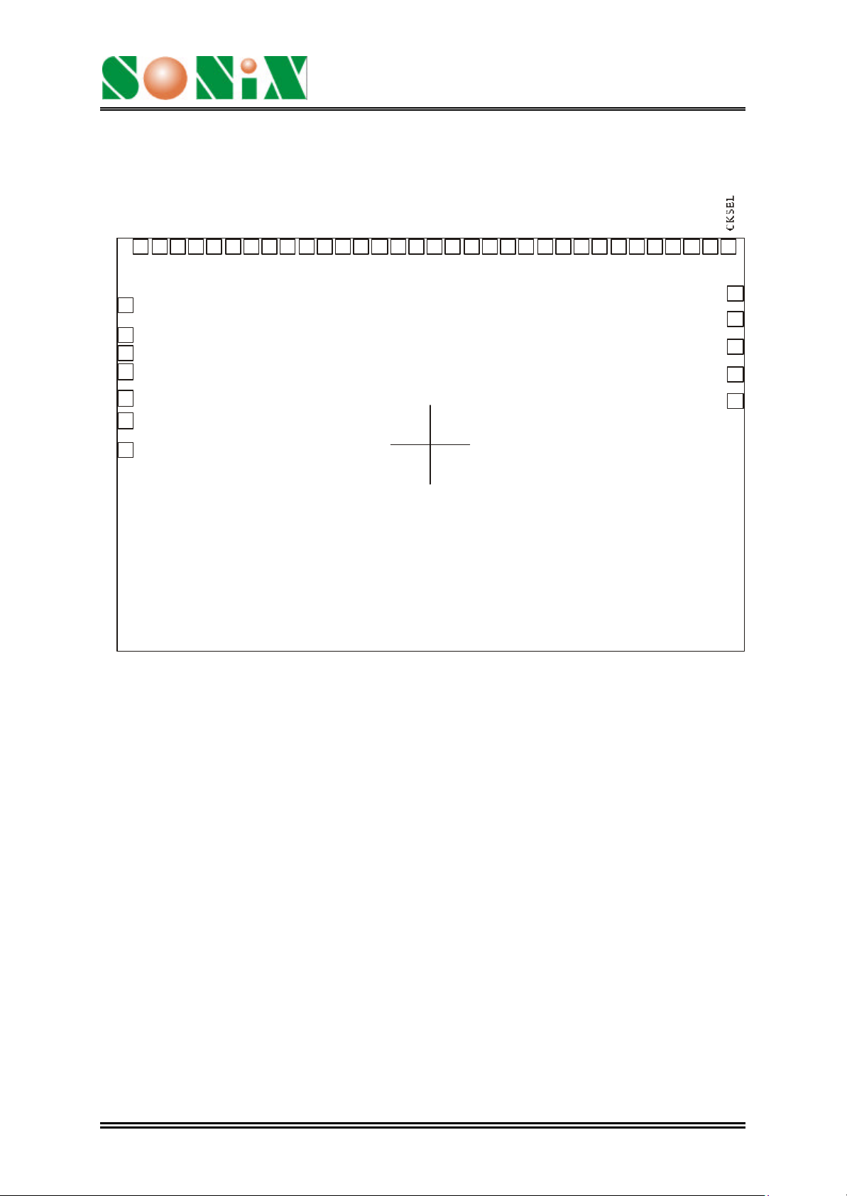
13. BONDING PAD
P1.7
P1.6
P1.5
P1.4
3738
XOUT
39
XIN
40
GND
41
VO
42
VDD
43
LXIN
44
LXOUT
45
SNC745
16-bit Voice Processor
P1.3
P1.2
GND
CVDD
P1.1
P1.0
P0.15
P0.14
P0.13
P0.12
P0.11
VDD
P0.10
P0.9
P0.8
P0.7
P0.6
P0.5
P0.4
CVDD
GND
RST
P0.3
P0.2
VDD
P0.1
P0.0
TEST
30313233343536
1011121314151617181920212223242526272829
(0.00,0.00)
6789
GND
5
BN0
4
VDD
3
BP0
2
GND
1
Note: The substrate MUST be connected to Vss in PCB layout.
Ver. 1.3 October 23, 2002
14
Page 15
SNC745
16-bit Voice Processor
DISCLAIMER
The information appearing in SONiX web pages (“this publication”) is believed to be
accurate.
However, this publication could contain technical inaccuracies or typographical errors.
The reader should not assume that this publication is error-free or that it will be suitable for
any particular purpose. SONiX makes no warranty, express, statutory implied or by
description in this publication or other documents which are referenced by or linked to this
publication. In no event shall SONiX be liable for any special, incidental, indirect or
consequential damages of any kind, or any damages whatsoever, including, without
limitation, those resulting from loss of use, data or profits, whether or not advised of the
possibility of damage, and on any theory of liability, arising out of or in connection with the
use or performance of this publication or other documents which are referenced by or
linked to this publication.
This publication was developed for products offered in Taiwan. SONiX may not offer the
products discussed in this document in other countries. Information is subject to change
without notice. Please contact SONiX or its local representative for information on
offerings available. Integrated circuits sold by SONiX are covered by the warranty and
patent indemnification provisions stipulated in the terms of sale only.
The application circuits illustrated in this document are for reference purposes only.
SONIX DISCLAIMS ALL WARRANTIES, INCLUDING THE WARRANTY OF
MERCHANTABILITY OR FITNESS FOR ANY PURPOSE. SONIX reserves the right to
halt production or alter the specifications and prices, and discontinue marketing the
Products listed at any time without notice. Accordingly, the reader is cautioned to verify
that the data sheets and other information in this publication are current before placing
orders.
Products described herein are intended for use in normal commercial applications.
Applications involving unusual environmental or reliability requirements, e.g. military
equipment or medical life support equipment, are specifically not recommended without
additional processing by SONIX for such application.
Ver. 1.3 October 23, 2002
15
 Loading...