

Page 1
SN75LVDS86A
FLATLINK RECEIVER
SLLS318A – NOVEMBER 1998 – REVISED MA Y 1999
D
3:21 Data Channel Expansion at up to
163 Million Bytes per Second Throughput
D
Suited for SVGA, XGA, or SXGA Display
Data Transmission From Controller to
Display With V ery Low EMI
D
3 Data Channels and Clock Low-Voltage
Differential Channels In and 21 Data and
Clock Low-Voltage TTL Channels Out
D
Operates From a Single 3.3-V Supply
D
T olerates 4-kV HBM ESD
D
Packaged in Thin Shrink Small-Outline
Package (TSSOP) With 20-Mil Terminal
Pitch
D
Consumes Less Than 1 mW When Disabled
D
Wide Phase-Lock Input Frequency Range
31 MHz to 68 MHz
D
No External Components Required for PLL
D
Inputs Meet or Exceed the Standard
Requirements of ANSI EIA/TIA-644
Standard
D
Improved Replacement for the DS90C364
and SN75LVDS86
D
Improved Jitter Tolerance
description
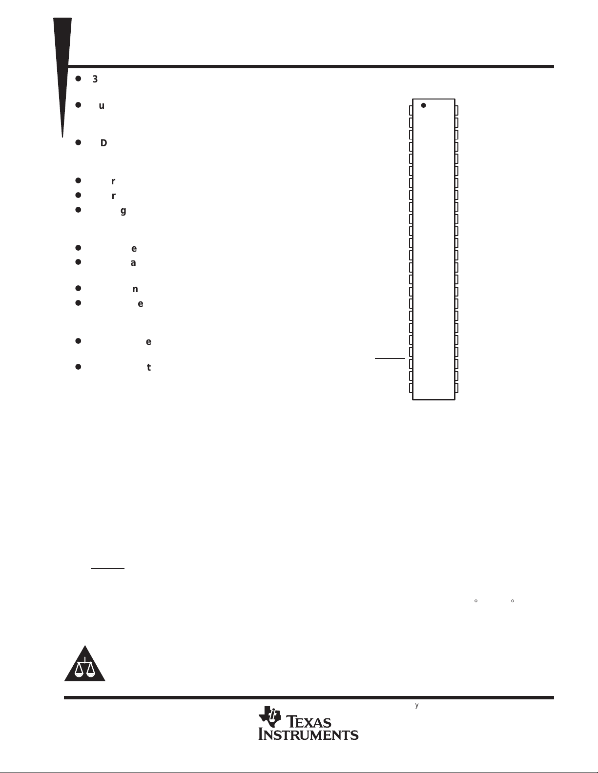
D17
D18
GND
D19
D20
NC
L VDSGND
A0M
A0P
A1M
A1P
L VDSV
CC
L VDSGND
A2M
A2P
CLKINM
CLKINP
L VDSGND
PLLGND
PLL V
CC
PLLGND
SHTDN
CLKOUT
D0
DGG PACKAGE
(TOP VIEW)
1
48
2
47
3
46
4
45
5
44
6
43
7
42
8
41
9
40
10
39
11
38
12
37
13
36
14
35
15
34
16
33
17
32
18
31
19
30
20
29
21
28
22
27
23
26
24
25
V
CC
D16
D15
D14
GND
D13
V
CC
D12
D1 1
D10
GND
D9
V
CC
D8
D7
D6
GND
D5
D4
D3
V
CC
D2
D1
GND
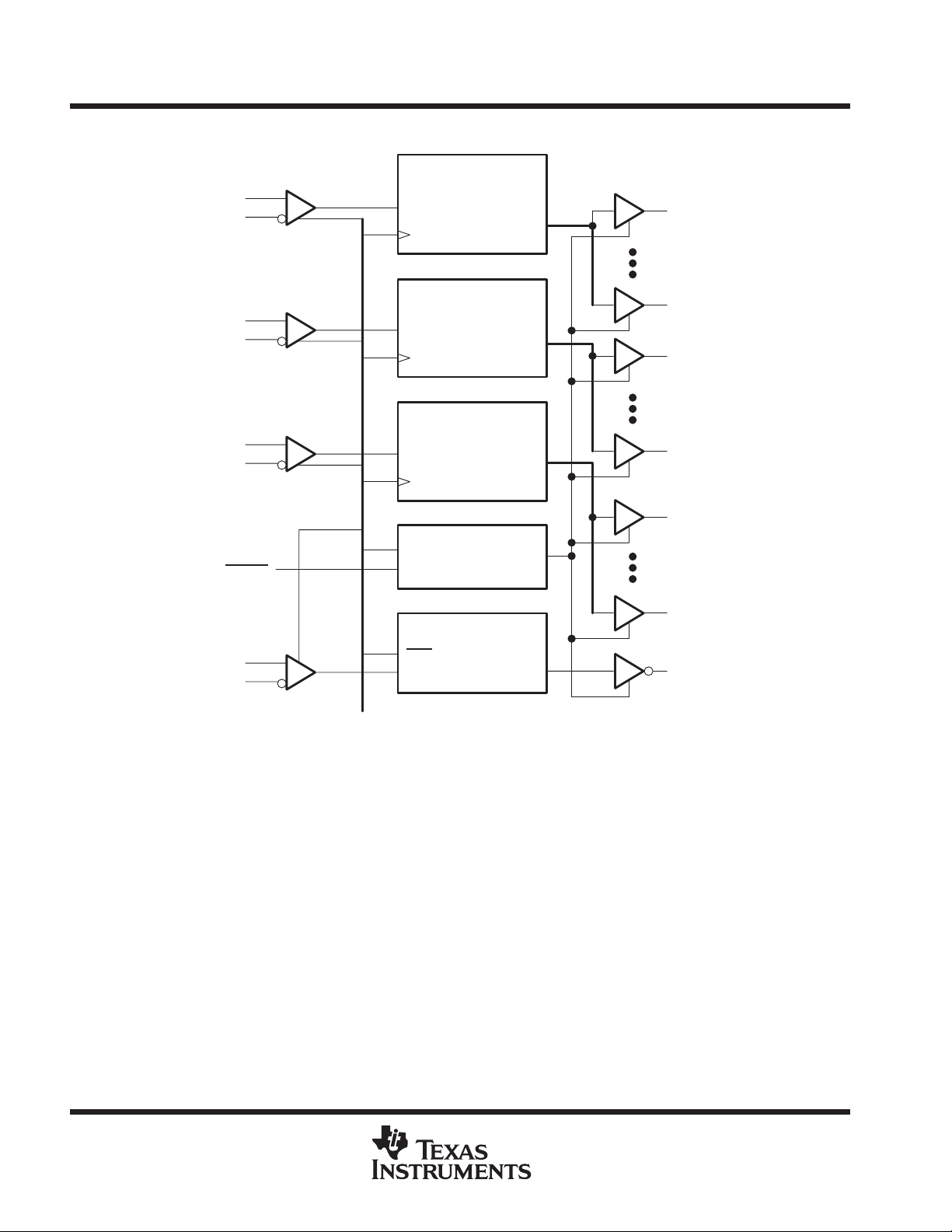
The SN75LVDS86A FlatLink receiver contains
NC – Not connected
three serial-in 7-bit parallel-out shift registers and
four low-voltage differential signaling (LVDS) line
receivers in a single integrated circuit. These
functions allow receipt of synchronous data from a compatible transmitter, such as the SN75LVDS81, ’83, ’84,
or ’85, over four balanced-pair conductors and expansion to 21 bits of single-ended low-voltage LVTTL
synchronous data at a lower transfer rate.
When receiving, the high-speed L VDS data is received and loaded into registers at seven times the L VDS input
clock (CLKIN) rate. The data is then unloaded to a 21-bit wide LVTTL parallel bus at the CLKIN rate. The
SN75LVDS86A presents valid data on the falling edge of the output clock (CLKOUT).
The SN75L VDS86A requires only four line-termination resistors for the differential inputs and little or no control.
The data bus appears the same at the input to the transmitter and output of the receiver with the data
transmission transparent to the user(s). The only user intervention is the possible use of the shutdown/clear
(SHTDN
) active-low input to inhibit the clock and shut off the LVDS receivers for lower power consumption. A
low level on this signal clears all internal registers to a low level.
The SN75LVDS86A is characterized for operation over ambient free-air temperatures of 0_C to 70_C.
Please be aware that an important notice concerning availability, standard warranty, and use in critical applications of
Texas Instruments semiconductor products and disclaimers thereto appears at the end of this data sheet.
FlatLink is a trademark of Texas Instruments Incorporated.
PRODUCTION DATA information is current as of publication date.
Products conform to specifications per the terms of Texas Instruments
standard warranty. Production processing does not necessarily include
testing of all parameters.
Copyright 1999, Texas Instruments Incorporated
POST OFFICE BOX 655303 • DALLAS, TEXAS 75265
1
Page 2
SN75LVDS86A
FLATLINK RECEIVER
SLLS318A – NOVEMBER 1998 – REVISED MA Y 1999
functional block diagram
A0P
A0M
A1P
A1M
A2P
A2M
Serial-In/Parallel-
Out Shift Register
Serial In
CLK
Serial-In/Parallel-
Out Shift Register
Serial In
CLK
Serial-In/Parallel-
Out Shift Register
Serial In
CLK
A, B, ...G
A, B, ...G
A, B, ...G
D0
D1
D2
D3
D4
D5
D6
D7
D8
D9
D10
D11
D12
D13
SHTDN
CLKINP
CLKINM
Input Bus
Control Logic
Clock Generator
CLK
Clock In
Clock Out
D14
D15
D16
D17
D18
D19
D20
CLKOUT
2
POST OFFICE BOX 655303 • DALLAS, TEXAS 75265
Page 3
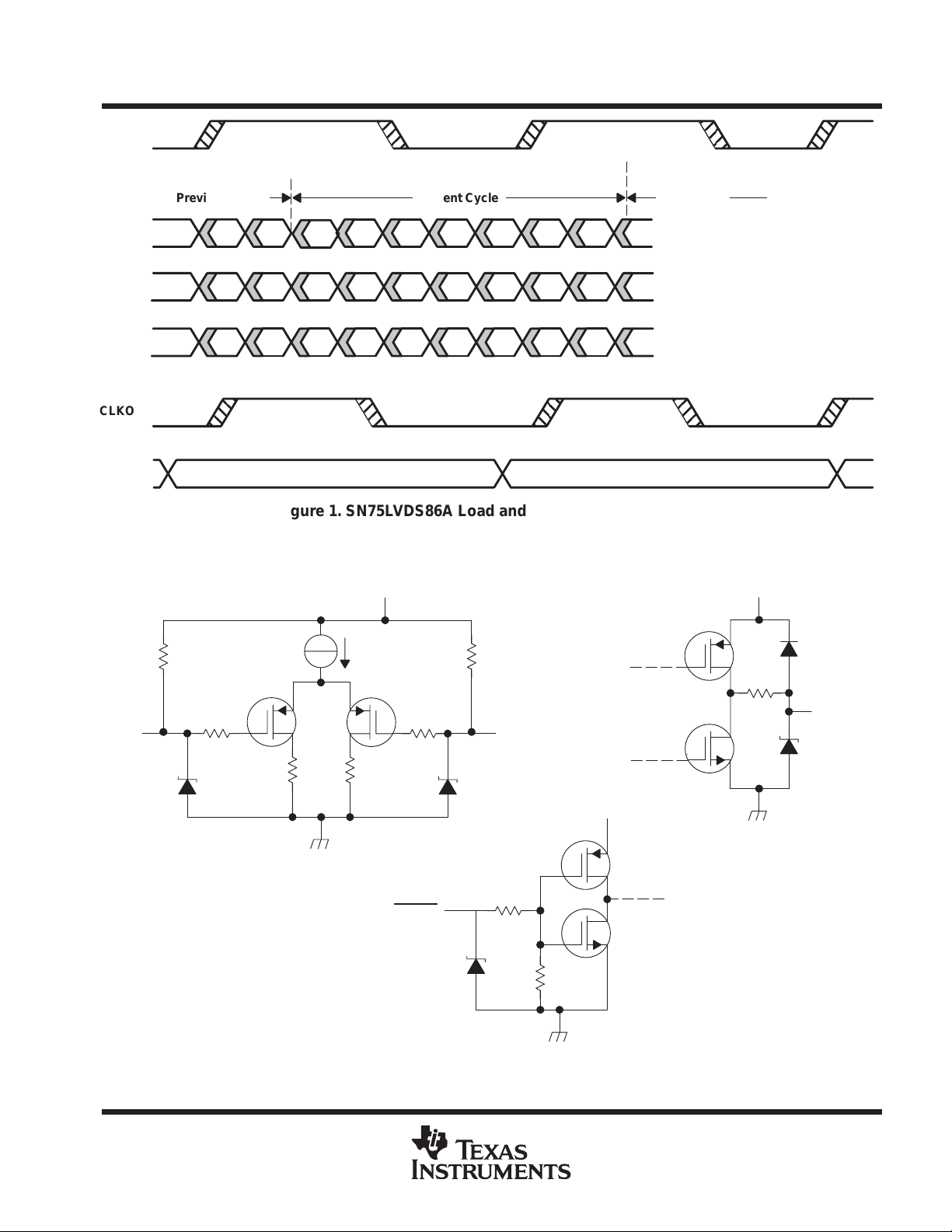
CLKIN
SN75LVDS86A
FLATLINK RECEIVER
SLLS318A – NOVEMBER 1998 – REVISED MA Y 1999
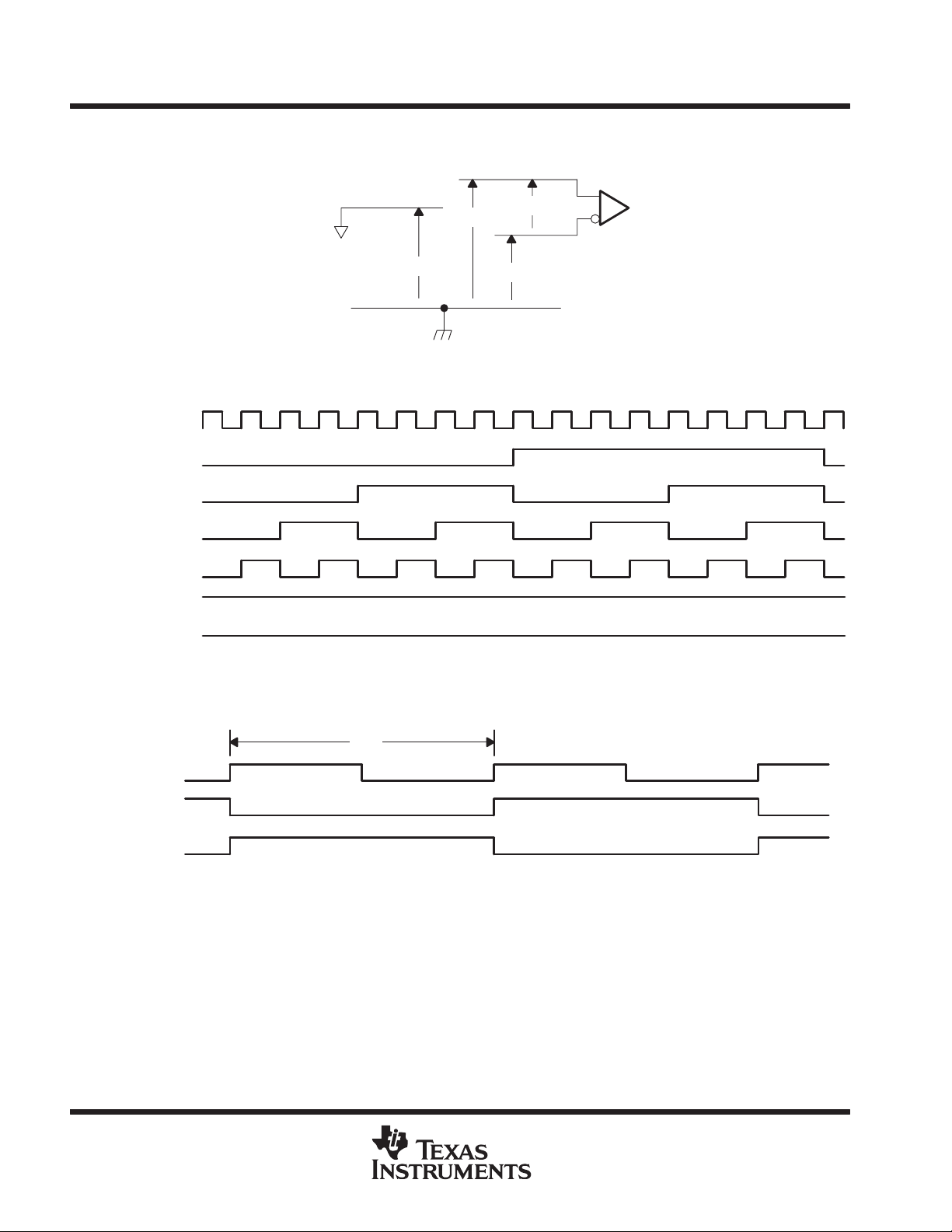
Current CyclePrevious Cycle Next Cycle
A0
A1
A2
CLKOUT
D0
D0–1 D6 D4 D3 D2 D1 D0 D6+1
D7–1 D13 D12 D11 D10 D9 D8 D7 D13+1
D14–1 D20 D19 D18 D17 D16 D15 D14 D20+1
D5
Dn – 1 Dn Dn + 1
Figure 1. SN75LVDS86A Load and Shift Timing Sequences
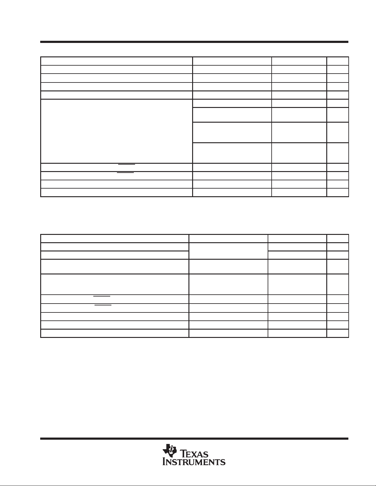
equivalent input and output schematic diagrams
V
CC
300 kΩ
300 kΩ
V
5 Ω
CC
AnP
100 Ω
7 V
INPUT
100 Ω
SHTDN
7 V
AnM
50 Ω
7 V
300 kΩ
INPUT
D Output
7 V
V
CC
OUTPUT
POST OFFICE BOX 655303 • DALLAS, TEXAS 75265
3
Page 4
SN75LVDS86A
FLATLINK RECEIVER
SLLS318A – NOVEMBER 1998 – REVISED MA Y 1999
absolute maximum ratings over operating free-air temperature range (unless otherwise noted)
Supply voltage range, V
Voltage range at any terminal –0.5 V to V
Electrostatic discharge (see Note 2): All pins (Class 3A) 4 KV. . . . . . . . . . . . . . . . . . . . . . . . . . . . . . . . . . . . . . . .
Continuous total power dissipation See Dissipation Rating Table. . . . . . . . . . . . . . . . . . . . . . . . . . . . . . . . . . . . . .
Storage temperature range, T
Lead temperature 1,6 mm (1/16 inch) from case for 10 seconds 260_C. . . . . . . . . . . . . . . . . . . . . . . . . . . . . . . .
†
Stresses beyond those listed under “absolute maximum ratings” may cause permanent damage to the device. These are stress ratings only, and
functional operation of the device at these or any other conditions beyond those indicated under “recommended operating conditions” is not
implied. Exposure to absolute-maximum-rated conditions for extended periods may affect device reliability.
NOTES: 1. All voltage values are with respect to the GND terminals unless otherwise noted.
2. This rating is measured using MIL-STD-883C Method, 3015.7.
PACKAGE
DGG 1316 mW 13.1 mW/°C 726 mW
‡
This is the inverse of the junction-to-ambient thermal resistance when board mounted and with
no air flow.
(see Note 1) –0.5 V to 4 V. . . . . . . . . . . . . . . . . . . . . . . . . . . . . . . . . . . . . . . . . . . . . . . . . . . .
CC
All pins (Class 2B) 200 V. . . . . . . . . . . . . . . . . . . . . . . . . . . . . . . . . . . . . . .
stg
DISSIPATION RATING T ABLE
TA ≤ 25°C
POWER RATING
DERATING FACTOR
ABOVE TA = 25°C
‡
POWER RATING
TA = 70°C
+ 0.5 V. . . . . . . . . . . . . . . . . . . . . . . . . . . . . . . . . . . . . . . . . . . . . . . .
CC
–65_C to 150_C. . . . . . . . . . . . . . . . . . . . . . . . . . . . . . . . . . . . . . . . . . . . . . . . . . .
recommended operating conditions (see Figure 2)
MIN NOM MAX UNIT
Supply voltage, V
High-level input voltage, VIH (SHTDN) 2 V
Low-level input voltage, VIL (SHTDN) 0.8 V
Magnitude differential input voltage, |VID| 0.1 0.6 V
Common-mode input voltage, V
Operating free-air temperature, T
CC
IC
A
3 3.3 3.6 V
|VID|
2
0 70 °C
2.4
*
|VID|
2
V
†
timing requirements
Cycle time, input clock, t
§
Parameter tc is defined as the mean duration of a minimum of 32000 clock cycles.
4
§
c
POST OFFICE BOX 655303 • DALLAS, TEXAS 75265
MIN NOM MAX UNIT
14.7 tc32.4 ns
Page 5
C
See Figure 5
SN75LVDS86A
FLATLINK RECEIVER
SLLS318A – NOVEMBER 1998 – REVISED MA Y 1999
electrical characteristics over recommended operating conditions (unless otherwise noted)
PARAMETER TEST CONDITIONS MIN TYP†MAX UNIT
V
IT+
V
IT–
V
OH
V
OL
I
CC
I
IH
I
IL
I
I
I
OZ
†
All typical values are at VCC = 3.3 V, TA = 25°C.
‡
The algebraic convention, in which the less-positive (more-negative) limit is designated minimum, is used in this data sheet for the negative-going
input voltage threshold only .
Positive-going differential input threshold voltage 100 mV
Negative-going differential input threshold voltage
High-level output voltage IOH = –4 mA 2.4 V
Low-level output voltage IOL = 4 mA 0.4 V
Quiescent current (average)
High-level input current (SHTDN) VIH = V
Low-level input current (SHTDN) VIL = 0 ±20 µA
Input current A inputs 0 ≤ VI ≤ 2.4 V ±20 µA
High-impedance output current VO = 0 or V
‡
Disabled, All inputs to GND 280 µA
Enabled,
AnM = 1.4 V,
Enabled, CL = 8 pF,
Grayscale pattern (see Figure 3),
tc = 15.38 ns
Enabled, CL = 8 pF,
Worst-case pattern (see Figure 4)
tc = 15.38 ns
AnP = 1 V,
tc = 15.38 ns
CC
CC
–100 mV
33 40 mA
43 mA
68 mA
±20 µA
±10 µA
switching characteristics over recommended operating conditions (unless otherwise noted)
PARAMETER TEST CONDITIONS MIN TYP†MAX UNIT
t
su
t
h
t
(RSKM)
t
d
t
en
t
dis
t
t
t
t
t
w
†
All typical values are at VCC = 3.3 V, TA = 25°C.
§
The parameter t
parameter at clock periods other than 15.38 ns can be calculated from t
¶
|Input clock jitter| is the magnitude of the change in input clock period.
Setup time, D0 – D20 to CLKOUT↓
Data hold time, CLKOUT↓ to D0 – D20
Receiver input skew margin§ (see Figure 7)
Delay time, CLKIN↑ to CLKOUT↓
(see Figure 7)
Enable time, SHTDN to phase lock
Disable time, SHTDN to off state
Transition time, output (10% to 90% tr or tf) (data only) CL = 8 pF 3 ns
Transition time, output (10% to 90% tr or tf) (clock only) CL = 8 pF 1.5 ns
Pulse duration, output clock 0.50 t
is the timing margin available to allocate to the transmitter and interconnection skews and clock jitter. The value of this
(RSKM)
p
= 8 pF,
L
tc = 15.38 ns (±0.2%),
|Input clock jitter| < 50 ps¶,
VCC = 3.3 V,
tc = 15.38 ns (±0.2%),
TA = 25°C
See Figure 7 1 ms
See Figure 8 400 ns
= tc/14 – 550 ps.
RSKM
5 ns
5 ns
550 700 ps
3 5 7 ns
c
ns
POST OFFICE BOX 655303 • DALLAS, TEXAS 75265
5
Page 6
SN75LVDS86A
FLATLINK RECEIVER
SLLS318A – NOVEMBER 1998 – REVISED MA Y 1999
PARAMETER MEASUREMENT INFORMATION
(V
IAP
CLKIN/CLKOUT
D0, 6, 12
V
IAP
+ V
)/2
IAM
V
IC
Figure 2. Voltage Definitions
V
IAM
AP
V
ID
AM
D1, 7, 13
D2, 8, 14
D3, 9, 15
D18, 19, 20
ALL OTHERS
NOTE A: The 16-grayscale test-pattern test device power consumption for a typical display pattern.
Figure 3. 16-Grayscale Test-Pattern Waveforms
t
c
CLKIN/CLKOUT
Even Dn
Odd Dn
NOTE A: The worst-case test pattern produces nearly the maximum switching frequency for all of the LVTTL outputs.
Figure 4. Worst-Case Test-Pattern Waveforms
6
POST OFFICE BOX 655303 • DALLAS, TEXAS 75265
Page 7
SN75LVDS86A
FLATLINK RECEIVER
SLLS318A – NOVEMBER 1998 – REVISED MA Y 1999
PARAMETER MEASUREMENT INFORMATION
t
su
70% V
OH
D0–D20
30% V
OH
t
h
70% V
OH
CLKOUT
30% V
OH
Figure 5. Setup and Hold Time Waveforms
POST OFFICE BOX 655303 • DALLAS, TEXAS 75265
7
Page 8

SN75LVDS86A
(
)
FLATLINK RECEIVER
SLLS318A – NOVEMBER 1998 – REVISED MA Y 1999
PARAMETER MEASUREMENT INFORMATION
An
and An
CLKIN
CLKOUT
Tektronix
HFS9003/HFS9DG1
Stimulus System
(repeating patterns of
11101 11 and 0001000)
4
±
tct
7
3
tct
7
(see Note A)
(RSKM)
(see Note A)
±
(RSKM)
An D0 – D20
Device
Under
Test
t
h1
(DUT)
CLKOUT
CLKIN
t
c
t
su1
t
d
t
W
Tektronix
Microwave Logic
Multi-BERT-100RX
Word Error Detector
Internal Strobing Position
tr < 1 ns
CLKIN
or An
10%
t
CLKOUT
NOTE A: CLKIN is advanced or delayed with respect to data until errors are observed at the receiver outputs. The advance or delay is then
reduced until there are no data errors observed. The magnitude of the advance or delay is t
90%
t
d
W
≈300 mV
0 V
≈–300 mV
V
OH
1.4 V
V
OL
RSKM
.
Figure 6. Receiver Input Skew Margin, Setup/Hold Time, and Delay Time Definitions
8
POST OFFICE BOX 655303 • DALLAS, TEXAS 75265
Page 9

CLKIN
SHTDN
An
SLLS318A – NOVEMBER 1998 – REVISED MA Y 1999
PARAMETER MEASUREMENT INFORMATION
t
en
SN75LVDS86A
FLATLINK RECEIVER
Dn
CLKIN
SHTDN
CLKOUT
Figure 7. Enable Time Waveforms
t
dis
Figure 8. Disable Time Waveforms
ValidInvalid
POST OFFICE BOX 655303 • DALLAS, TEXAS 75265
9
Page 10
SN75LVDS86A
FLATLINK RECEIVER
SLLS318A – NOVEMBER 1998 – REVISED MA Y 1999
60
55
50
45
TYPICAL CHARACTERISTICS
SUPPLY CURRENT
vs
CLOCK FREQUENCY
VCC = 3.6 V
40
– Supply Current – mA
35
CC
I
30
VCC = 3 V
25
30 40 50 60 70
f
– Clock Frequency – MHz
clk
Grayscale Data Pattern
CL = 8 pF
TA = 25°C
VCC = 3.3 V
80 90
Figure 9. RMS Grayscale ICC vs Clock Frequency
10
POST OFFICE BOX 655303 • DALLAS, TEXAS 75265
Page 11
SN75LVDS86A
FLATLINK RECEIVER
SLLS318A – NOVEMBER 1998 – REVISED MA Y 1999
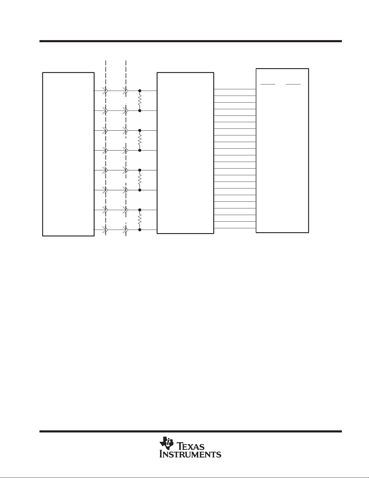
APPLICATION INFORMATION
Cable Flat Panel DisplayHost
SN75LVDS86ASN75LVDS84/5
41
Y0M
100 Ω
40
Y0P
39
Y1M
100 Ω
38
Y1P
35
Y2M
100 Ω
34
Y2P
CLKOUTM
CLKOUTP
NOTES: A. The four 100-Ω terminating resistors are recommended to be 0603 types.
B. NA – not applicable, these unused inputs should be left open.
33
100 Ω
32
8
9
10
11
14
15
16
17
A0M
A0P
A1M
A1P
A2M
A2P
CLKINM
CLKINP
D0
D1
D2
D3
D4
D5
D6
D7
D8
D9
D10
D11
D12
D13
D14
D15
D16
D17
D18
D19
D20
CLKOUT
24
26
27
29
30
31
33
34
35
37
39
40
41
43
45
46
47
1
2
4
5
23
Graphics Controller
12-BIT
RED0 RED0
RED1 RED1
RED2 RED2
RED3 RED3
NA RED4
NA RED5
GREEN0 GREEN0
GREEN1 GREEN1
GREEN2 GREEN2
GREEN3 GREEN3
NA GREEN4
NA GREEN5
BLUE0 BLUE0
BLUE1 BLUE1
BLUE2 BLUE2
BLUE3 BLUE3
NA BLUE4
NA BLUE5
H_SYNC H_SYNC
V_SYNC V_SYNC
ENABLE ENABLE
CLOCK CLOCK
18-BIT
Figure 10. 18-Bit Color Host to Flat Panel Display Application
POST OFFICE BOX 655303 • DALLAS, TEXAS 75265
11
Page 12

SN75LVDS86A
FLATLINK RECEIVER
SLLS318A – NOVEMBER 1998 – REVISED MA Y 1999
Cable Flat Panel DisplayHost
APPLICATION INFORMATION
Y0M
Y0P
Y1M
Y1P
Y2M
Y2P
CLKOUTM
CLKOUTP
Y3M
48
47
46
45
42
41
40
39
38
100 Ω
100 Ω
100 Ω
100 Ω
8
9
10
11
14
15
16
17
SN75LVDS86ASN75LVDS81/83
A0M
A0P
A1M
A1P
A2M
A2P
CLKINM
CLKINP
D0
D1
D2
D3
D4
D5
D6
D7
D8
D9
D10
D11
D12
D13
D14
D15
D16
D17
D18
D19
D20
CLKOUT
24
26
27
29
30
31
33
34
35
37
39
40
41
43
45
46
47
1
2
4
5
23
Graphics Controller
12-BIT
RED0 RED0
RED1 RED1
RED2 RED2
RED3 RED3
NA RED4
NA RED5
GREEN0 GREEN0
GREEN1 GREEN1
GREEN2 GREEN2
GREEN3 GREEN3
NA GREEN4
NA GREEN5
BLUE0 BLUE0
BLUE1 BLUE1
BLUE2 BLUE2
BLUE3 BLUE3
NA BLUE4
NA BLUE5
H_SYNC H_SYNC
V_SYNC V_SYNC
ENABLE ENABLE
CLOCK CLOCK
18-BIT
37
Y3P
NOTES: A. The four 100-Ω terminating resistors are recommended to be 0603 types.
B. NA – not applicable, these unused inputs should be left open.
Figure 11. 24-Bit Color Host to 18-Bit Color LCD Panel Display Application
See the
FLatLink Designer’s Guide
(SLLA012) for more application information.
12
POST OFFICE BOX 655303 • DALLAS, TEXAS 75265
Page 13
SN75LVDS86A
FLATLINK RECEIVER
SLLS318A – NOVEMBER 1998 – REVISED MA Y 1999
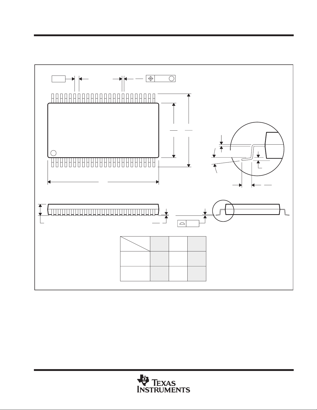
MECHANICAL INFORMATION
DGG (R-PDSO-G**) PLASTIC SMALL-OUTLINE PACKAGE
48 PIN SHOWN
0,50
48
1
1,20 MAX
0,27
0,17
25
24
A
0,15
0,05
0,08
M
6,20
8,30
6,00
7,90
Seating Plane
0,10
0,15 NOM
Gage Plane
0,25
0°–8°
0,75
0,50
DIM
NOTES: A. All linear dimensions are in millimeters.
B. This drawing is subject to change without notice.
C. Body dimensions do not include mold protrusion not to exceed 0,15.
D. Falls within JEDEC MO-153
PINS **
A MAX
A MIN
48
12,60
12,40
56
14,10
13,90
64
17,10
16,90
4040078/F 12/97
POST OFFICE BOX 655303 • DALLAS, TEXAS 75265
13
Page 14

IMPORTANT NOTICE
T exas Instruments and its subsidiaries (TI) reserve the right to make changes to their products or to discontinue
any product or service without notice, and advise customers to obtain the latest version of relevant information
to verify, before placing orders, that information being relied on is current and complete. All products are sold
subject to the terms and conditions of sale supplied at the time of order acknowledgement, including those
pertaining to warranty, patent infringement, and limitation of liability.
TI warrants performance of its semiconductor products to the specifications applicable at the time of sale in
accordance with TI’s standard warranty. Testing and other quality control techniques are utilized to the extent
TI deems necessary to support this warranty . Specific testing of all parameters of each device is not necessarily
performed, except those mandated by government requirements.
CERT AIN APPLICATIONS USING SEMICONDUCTOR PRODUCTS MAY INVOLVE POTENTIAL RISKS OF
DEATH, PERSONAL INJURY, OR SEVERE PROPERTY OR ENVIRONMENTAL DAMAGE (“CRITICAL
APPLICATIONS”). TI SEMICONDUCTOR PRODUCTS ARE NOT DESIGNED, AUTHORIZED, OR
WARRANTED TO BE SUITABLE FOR USE IN LIFE-SUPPORT DEVICES OR SYSTEMS OR OTHER
CRITICAL APPLICA TIONS. INCLUSION OF TI PRODUCTS IN SUCH APPLICATIONS IS UNDERST OOD TO
BE FULLY AT THE CUSTOMER’S RISK.
In order to minimize risks associated with the customer’s applications, adequate design and operating
safeguards must be provided by the customer to minimize inherent or procedural hazards.
TI assumes no liability for applications assistance or customer product design. TI does not warrant or represent
that any license, either express or implied, is granted under any patent right, copyright, mask work right, or other
intellectual property right of TI covering or relating to any combination, machine, or process in which such
semiconductor products or services might be or are used. TI’s publication of information regarding any third
party’s products or services does not constitute TI’s approval, warranty or endorsement thereof.
Copyright 1999, Texas Instruments Incorporated
 Loading...