

Page 1
SN75LV4737A
3.3-V/5-V MULTICHANNEL RS-232 LINE DRIVER/RECEIVER
SLLS178D – APRIL 1994 – REVISED FEBRUARY 2000
1
POST OFFICE BOX 655303 • DALLAS, TEXAS 75265
D
Single-Chip and Single-Supply Interface for
IBM PC/A T Serial Port
D
Meets or Exceeds the Requirements of
TIA/EIA-232-F and ITU v.11 Standards
D
Operates With 3.3-V or 5-V Supplies
D
One Receiver Remains Active During
Standby (Wake-up Mode)
D
Designed to Operate at 128 kbit/s Over a
3-m Cable
D
Low Standby Current ...5 µA Max
D
ESD Protection on RS-232 Pins Meets or
Exceeds 4 kV (HBM) and 1.5 kV (HBM) on
All Pins Per MIL-STD-883, Method 3015
D
External Capacitors . . . 0.1 µF
(VCC = 3.3 V . . . Five External Capacitors)
(VCC = 5 V . . . Four External Capacitors)
D
Accepts 5-V Logic Input With 3.3-V Supply
D
Applications
– RS-232 Interface
– Battery-Powered Systems, PDAs
– Notebook, Laptop, and Palmtop PCs
– External Modems and Hand-Held
Terminals
D
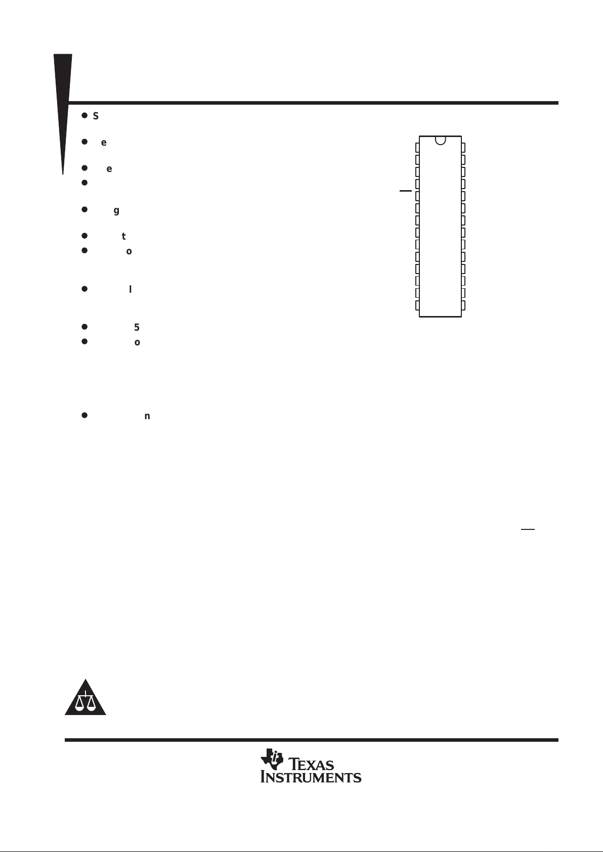
Packaged in Shrink Small-Outline Package
description
The SN75L V4737A
‡
consists of three line drivers, five line receivers, and a charge-pump circuit. It provides the
electrical interface between an asynchronous communication controller and the serial-port connector, and
meets the requirements of TIA/EIA-232-F . This combination of drivers and receivers matches those needed for
the typical serial port used in an IBM PC/A T or compatibles. The charge pump and five small external capacitors
allow operation from a single 3.3-V supply, and four capacitors allow operation from a 5-V supply.
The device has flexible control options for power management when the serial port is inactive. A common
disable for all of the drivers and receivers is provided with the active-high STBY input. The active-low EN
input
is an enable for one receiver to implement a wake-up feature for the serial port. All the logic inputs can accept
signals from controllers operating from a 5-V supply, even though the SN75LV4737A is operating from 3.3 V.
The SN75LV4737A is characterized for operation over the temperature range of 0°C to 70°C.
Copyright 2000, Texas Instruments Incorporated
PRODUCTION DATA information is current as of publication date.
Products conform to specifications per the terms of Texas Instruments
standard warranty. Production processing does not necessarily include
testing of all parameters.
Please be aware that an important notice concerning availability, standard warranty, and use in critical applications of
Texas Instruments semiconductor products and disclaimers thereto appears at the end of this data sheet.
‡
Patent-pending design
IBM and PC/AT are trademarks of International Business Machines Corporation.
1
2
3
4
5
6
7
8
9
10
11
12
13
14
28
27
26
25
24
23
22
21
20
19
18
17
16
15
V
DD
C2+
V
CC
C2–
EN
C1+
DIN1
DIN2
DIN3
ROUT1
ROUT2
ROUT3
ROUT4
ROUT5
C3+
GND
C3–
V
SS
C1–
STBY
DOUT1
DOUT2
DOUT3
RIN1
RIN2
RIN3
RIN4
RIN5
DB PACKAGE
†
(TOP VIEW)
†
The DB package is only
available in left-ended tape and
reel (order part number
SN75LV4737ADBR).
Page 2
SN75LV4737A
3.3-V/5-V MULTICHANNEL RS-232 LINE DRIVER/RECEIVER
SLLS178D – APRIL 1994 – REVISED FEBRUARY 2000
2
POST OFFICE BOX 655303 • DALLAS, TEXAS 75265
Function Tables
EACH DRIVER
INPUTS
OUTPUT
DIN STBY
DOUT
X H Z
L LH
H LL
Open L L
H = high level, L = low level,
X = irrelevant, Z = high
impedance
EACH RECEIVER
INPUTS
OUTPUTS
STBY EN RIN5 RIN1–RIN4 ROUT5 ROUT1–ROUT4
H H X X Z Z
H LH X L Z
H LL X H Z
L XL L H H
L X H H L L
H = high level, L = low level, X = irrelevant, Z = high impedance
Page 3
SN75LV4737A
3.3-V/5-V MULTICHANNEL RS-232 LINE DRIVER/RECEIVER
SLLS178D – APRIL 1994 – REVISED FEBRUARY 2000
3
POST OFFICE BOX 655303 • DALLAS, TEXAS 75265
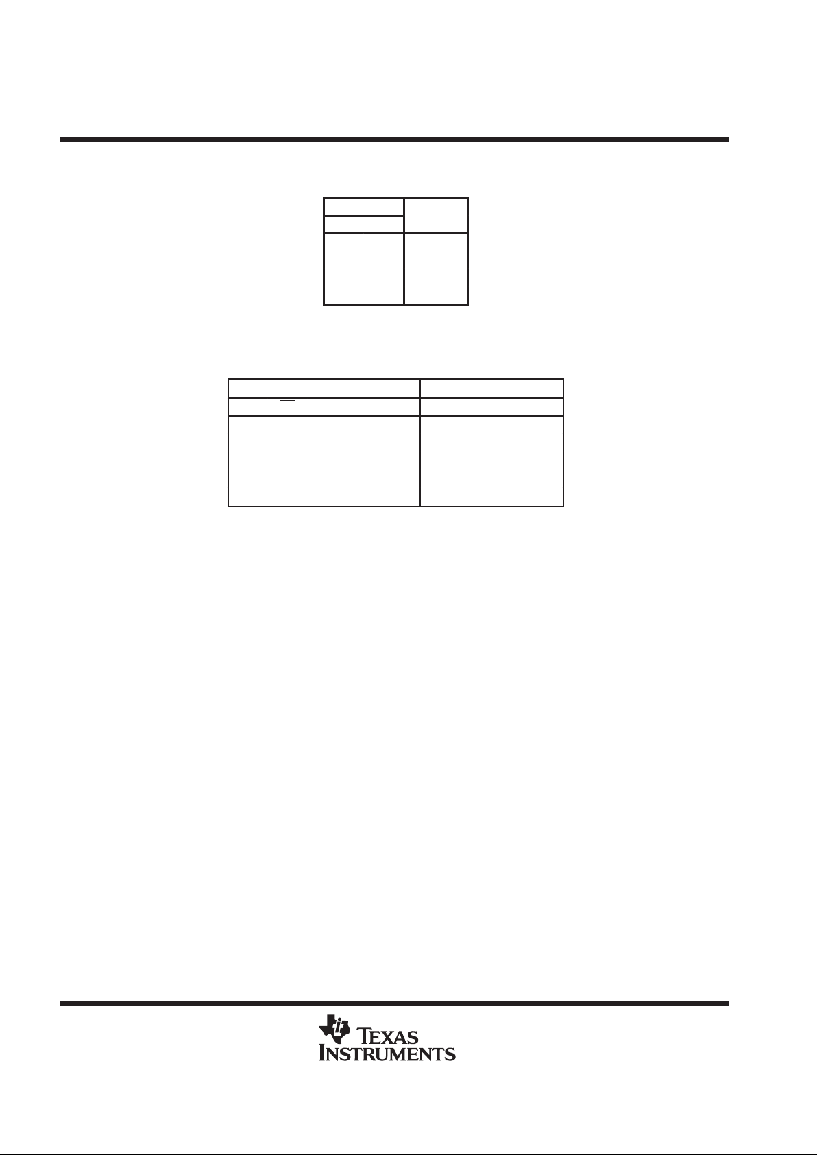
logic diagram (positive logic)
DIN1
DIN2
DIN3
RIN1
RIN2
RIN3
RIN4
RIN5
STBY
EN
DOUT1
DOUT2
DOUT3
ROUT1
ROUT2
ROUT3
ROUT4
ROUT5
7
8
9
19
18
17
16
15
23
5
22
21
20
10
11
12
13
14
Page 4
SN75LV4737A
3.3-V/5-V MULTICHANNEL RS-232 LINE DRIVER/RECEIVER
SLLS178D – APRIL 1994 – REVISED FEBRUARY 2000
4
POST OFFICE BOX 655303 • DALLAS, TEXAS 75265
schematics of inputs and outputs
STBY AND EN INPUTS
V
CC
GND
Input
V
SS
V
CC
GND
V
SS
TYPICAL RECEIVER INPUTS
V
CC
GND
TYPICAL DRIVER INPUTS
V
CC
GND
V
DD
TYPICAL OF ALL DRIVER OUTPUTS
TYPICAL OF ALL
RECEIVER OUTPUTS
V
SS
Output
300 Ω
Output
GND
5 kΩ
Input
Input
absolute maximum ratings over operating free-air temperature range (unless otherwise noted)
†
Supply voltage, VCC 7 V. . . . . . . . . . . . . . . . . . . . . . . . . . . . . . . . . . . . . . . . . . . . . . . . . . . . . . . . . . . . . . . . . . . . . . . .
Positive output supply voltage, VDD (see Note 1) 15 V. . . . . . . . . . . . . . . . . . . . . . . . . . . . . . . . . . . . . . . . . . . . . . .
Negative output supply voltage, V
SS
–15 V. . . . . . . . . . . . . . . . . . . . . . . . . . . . . . . . . . . . . . . . . . . . . . . . . . . . . . .
Input voltage range, VI: Driver –3 V to 7 V. . . . . . . . . . . . . . . . . . . . . . . . . . . . . . . . . . . . . . . . . . . . . . . . . . . . . . . . .
Receiver –30 V to 30 V. . . . . . . . . . . . . . . . . . . . . . . . . . . . . . . . . . . . . . . . . . . . . . . . . . . .
Output voltage range, VO: Driver VSS – 0.3 V to VDD + 0.3 V. . . . . . . . . . . . . . . . . . . . . . . . . . . . . . . . . . . . . . . .
Receiver –0.3 V to 7 V. . . . . . . . . . . . . . . . . . . . . . . . . . . . . . . . . . . . . . . . . . . . . . . . . .
Package thermal impedance, θ
JA
(see Note 2) 62°C/W. . . . . . . . . . . . . . . . . . . . . . . . . . . . . . . . . . . . . . . . . . . . .
Lead temperature 1,6 mm (1/16 inch) from case for 10 seconds 260°C. . . . . . . . . . . . . . . . . . . . . . . . . . . . . . .
Storage temperature range, T
stg
–65°C to 150°C. . . . . . . . . . . . . . . . . . . . . . . . . . . . . . . . . . . . . . . . . . . . . . . . . . .
†
Stresses beyond those listed under “absolute maximum ratings” may cause permanent damage to the device. These are stress ratings only, and
functional operation of the device at these or any other conditions beyond those indicated under “recommended operating conditions” is not
implied. Exposure to absolute-maximum-rated conditions for extended periods may affect device reliability.
NOTES: 1. All voltages are with respect to network GND.
2. The package thermal impedance is calculated in accordance with JESD 51.
Page 5

SN75LV4737A
3.3-V/5-V MULTICHANNEL RS-232 LINE DRIVER/RECEIVER
SLLS178D – APRIL 1994 – REVISED FEBRUARY 2000
5
POST OFFICE BOX 655303 • DALLAS, TEXAS 75265
recommended operating conditions
MIN NOM MAX UNIT
pp
VCC = 3.3 V 3 3.3 3.6 V
VCCSuppl
y v
oltage
VCC = 5 V 4.5 5 5.5 V
DIN, EN, STBY VCC = 3.3 V 2
V
IH
Driver high-level input voltage
DIN
2
V
EN, STBY
V
CC
=
5 V
2.5
V
IL
Driver low-level input voltage DIN, EN, STBY 0.8 V
V
I
Receiver input voltage ±30 V
External capacitor
3.3-V operation (C1, C2, C3, C4, C5),
5-V operation (C1, C3, C4, C5),
See Note 3 and Figures 6 and 7
0.1 µF
T
A
Operating free-air temperature 0 70 °C
NOTE 3: C2 is needed only for 3.3-V operation.
electrical characteristics over recommended ranges of supply voltage and operating free-air
temperature (see Figures 6 and 7) (unless otherwise noted)
VCC = 3.3 V VCC = 5 V
PARAMETER
TEST CONDITIONS
MIN TYP†MAX MIN TYP†MAX
UNIT
V
DD
Positive supply voltage No load 8 10 7 8.7 V
V
SS
Negative supply voltage No load –9.5 –7 –8 –6 V
I
I
Input current (EN, STBY) See Notes 4 and 5 ±2 ±2 µA
Supply current
STBY at GND,
EN
at VCC or GND
8.4 10 18 10 12 20.7 mA
I
CC
Supply current (standby mode)
(see Note 4)
No load,
Inputs open
EN, STBY at V
CC
5 5
Supply current (wake-up mode)
(see Note 5)
EN at GND,
STBY at V
CC
10 10
µ
A
†
All typical values are at VCC = 3.3 V or VCC = 5 V, and TA = 25°C.
NOTES: 4. When standby mode is not used, STBY input must be taken low.
5. When wake-up mode is not used, EN
input must be taken high.
Page 6

SN75LV4737A
3.3-V/5-V MULTICHANNEL RS-232 LINE DRIVER/RECEIVER
SLLS178D – APRIL 1994 – REVISED FEBRUARY 2000
6
POST OFFICE BOX 655303 • DALLAS, TEXAS 75265
DRIVER SECTION
electrical characteristics over recommended ranges of supply voltage and operating free-air
temperature (unless otherwise noted)
PARAMETER TEST CONDITIONS MIN
TYP
†
MAX UNIT
V
OH
High-level output voltage RL = 3 kΩ 5.5 7 V
V
OL
Low-level output voltage RL = 3 kΩ –6 –5 V
I
IH
High-level input current VI = V
CC
1 µA
I
IL
Low-level input current VI at GND –10 µA
p
VCC = 3.6 V, VO = 0 V
IOSShort-circuit output current (see Note 6)
VCC = 5.5 V, VO = 0 V
±15
±40
mA
r
o
Output resistance VCC = VDD = VSS = 0 V, VO = ±2 V 300 500 Ω
†
All typical values are at VCC = 3.3 V or VCC = 5 V, and TA = 25°C.
NOTE 6: Short-circuit durations should be controlled to prevent exceeding the device absolute maximum power dissipation ratings, and not more
than one output should be shorted at a time.
switching characteristics over recommended ranges of supply voltage and operating free-air
temperature (unless otherwise noted)
PARAMETER TEST CONDITIONS MIN TYP†MAX UNIT
p
p
VCC = 3.3 V 100 500 850
t
PLH
Propagation delay time, lo
w- to
high-level output
CL = 50 pF,
VCC = 5 V 100 500 850
ns
p
p
R
L
=
3 kΩ to 7 kΩ
,
See Fi
g
ure 1
VCC = 3.3 V 100 500 850
t
PHL
Propagation delay time, high- to low-level output
See Figure 1
VCC = 5 V 100 500 850
ns
t
PZH
Output enable time to high level
C
= 50 pF, R
= 3 kΩ to 7 kΩ,
1 5 ms
t
PZL
Output enable time to low level
L
,
See Figure 2
L
,
3 7 ms
p
VCC = 3.3 V 0.9 3
t
PHZ
Output disable time from high level
CL = 50 pF,
VCC = 5 V 0.6 3
µ
s
p
R
L
= 3 kΩ to 7 kΩ,
See
Figure 2
VCC = 3.3 V 0.5 3
t
PLZ
Output disable time from low level
See Figure 2
VCC = 5 V 0.3 3
µ
s
SR Slew rate
CL = 50 pF,
See Figure 1
RL = 3 kΩ to 7 kΩ,
4 30 V/µs
SR(tr) Slew rate, transition region
CL = 2500 pF,
See Figure 3
RL = 3 kΩ to 7 kΩ,
3 30 V/µs
†
All typical values are at VCC = 3.3 V or VCC = 5 V, and TA = 25°C.
Page 7

SN75LV4737A
3.3-V/5-V MULTICHANNEL RS-232 LINE DRIVER/RECEIVER
SLLS178D – APRIL 1994 – REVISED FEBRUARY 2000
7
POST OFFICE BOX 655303 • DALLAS, TEXAS 75265
RECEIVER SECTION
electrical characteristics over recommended ranges of supply voltage and operating free-air
temperature (unless otherwise noted)
PARAMETER TEST CONDITIONS MIN TYP†MAX UNIT
p
VCC = 3.3 V 2.4 3
VOHHigh-level output voltage
I
OH
= –2
mA
VCC = 5 V 3.5 5
V
V
OL
Low-level output voltage IOL = 2 mA 0.2 0.4 V
V
IT+
Positive-going input threshold voltage 2.2 2.6 V
V
IT–
Negative-going input threshold voltage 0.6 1 V
V
hys
Input hysteresis (V
IT+
– V
IT–
) 0.5 1.2 1.8 V
r
i
Input resistance VI = ±3 V to ±25 V 3 5 7 kΩ
†
All typical values are at VCC = 3.3 V or VCC = 5 V, and TA = 25°C.
switching characteristics over recommended ranges of supply voltage and operating free-air
temperature, C
L
= 50 pF, RL = 3 kΩ to GND
TEST
VCC = 3.3 V VCC = 5 V
PARAMETER
CONDITIONS
MIN TYP MAX MIN TYP MAX
UNIT
t
PLH
Propagation delay time, low- to high-level output 10 70 200 10 70 200 ns
t
PHL
Propagation delay time, high- to low-level output 10 60 200 10 55 200 ns
t
PLH
Propagation delay time, low- to high-level output
(wake-up mode)
See Figure 4
40 200 40 200 µs
t
PHL
Propagation delay time, high- to low-level output
(wake-up mode)
90 500 70 500 ns
t
PZH
Output enable time to high level 3 10 1.2 10 µs
t
PZL
Output enable time to low level
100 250 60 250 ns
t
PHZ
Output disable time from high level
See Figure 5
100 200 600 100 150 600 ns
t
PLZ
Output disable time from low level 130 250 60 250 ns
Page 8

SN75LV4737A
3.3-V/5-V MULTICHANNEL RS-232 LINE DRIVER/RECEIVER
SLLS178D – APRIL 1994 – REVISED FEBRUARY 2000
8
POST OFFICE BOX 655303 • DALLAS, TEXAS 75265
PARAMETER MEASUREMENT INFORMATION
CL = 50 pF
(see Note A)
50 Ω
TEST CIRCUIT VOLTAGE WAVEFORMS
10%
10%
90%
90%
0 V
3 V
50%50%
Output
Input
V
OL
V
OH
t
PHL
t
TLH
Generator
(see Note B)
R
L
0 V
STBY
RS-232
Output
t
PLH
t
THL
5 µs
SR
+
0.8 V
ǒ
VOH*
V
OL
Ǔ
t
TLH
or
0.8 V
ǒ
VOL*
V
OH
Ǔ
t
THL
NOTES: A. CL includes probe and jig capacitance.
B. The pulse generator has the following characteristics: ZO = 50 Ω, 50% duty cycle, tr ≤ 10 ns, tf ≤ 10 ns.
Figure 1. Driver Propagation Delay Times and Slew Rate (5-µs Input)
TEST CIRCUIT VOLTAGE WAVEFORMS
Output
t
PHZ
t
PLZ
t
PZH
t
PZL
5 V
Output
Input
50 Ω
Generator
(see Note B)
R
L
RS-232
Output
3 V or 0 V
CL = 50 pF
(see Note A)
STBY
NOTES: A. CL includes probe and jig capacitance.
B. The pulse generator has the following characteristics: ZO = 50 Ω, 50% duty cycle, tr ≤ 10 ns, tf ≤ 10 ns.
0 V
3 V
V
OH
V
OL
1.5 V 1.5 V
5 V
–5 V
–5 V
Figure 2. Driver Enable and Disable Test Times
Page 9

SN75LV4737A
3.3-V/5-V MULTICHANNEL RS-232 LINE DRIVER/RECEIVER
SLLS178D – APRIL 1994 – REVISED FEBRUARY 2000
9
POST OFFICE BOX 655303 • DALLAS, TEXAS 75265
PARAMETER MEASUREMENT INFORMATION
CL = 2500 pF
(see Note A)
50 Ω
TEST CIRCUIT VOLTAGE WAVEFORMS
0 V
3 V
Output
Input
V
OL
V
OH
t
TLH
Generator
(see Note B)
R
L
0 V
STBY
RS-232
Output
t
THL
20 µs
SR(tr)
+
6V
t
THL
or t
TLH
NOTES: A. CL includes probe and jig capacitance.
B. The pulse generator has the following characteristics: ZO = 50 Ω, 50% duty cycle, tr ≤ 10 ns, tf ≤ 10 ns.
1.5 V 1.5 V
3 V 3 V
–3 V
–3 V
Figure 3. Driver Transition Times and Slew Rate (20-µs Input)
TEST CIRCUIT VOLTAGE WAVEFORMS
50 Ω
Output
Input
t
PHL
Generator
(see Note B)
0 V
STBY
t
PLH
500 ns
3 V or 0 V
EN
CL = 50 pF
(see Note A)
NOTES: A. CL includes probe and jig capacitance.
B. The pulse generator has the following characteristics: PRR = 1 MHz, ZO = 50 Ω, 50% duty cycle, tr ≤ 10 ns, tf ≤ 10 ns.
1.5 V 1.5 V
0 V
3 V
V
OL
V
OH
50% 50%
R
L
RS-232
Output
Figure 4. Receiver Propagation Delay Times
Page 10

SN75LV4737A
3.3-V/5-V MULTICHANNEL RS-232 LINE DRIVER/RECEIVER
SLLS178D – APRIL 1994 – REVISED FEBRUARY 2000
10
POST OFFICE BOX 655303 • DALLAS, TEXAS 75265
PARAMETER MEASUREMENT INFORMATION
TEST CIRCUIT VOLTAGE WAVEFORMS
50 Ω
Generator
(see Note B)
3 V or 0 V
Output
V
OL
V
OH
t
PZH
(S1 at GND)
3 V
0 V
0.3 V
Output
Input
25 µs
3 V or 0 V
EN
STBY
R
L
S1
V
CC
GND
CL = 50 pF
(see Note A)
Output
NOTES: A. CL includes probe and jig capacitance.
B. The pulse generator has the following characteristics: PRR = 1 MHz, ZO = 50 Ω, 50% duty cycle, tr ≤ 10 ns, tf ≤ 10 ns.
50% 50%
50% 50%
1.5 V 1.5 V
t
PHZ
(S1 at GND)
t
PLZ
(S1 at VCC)
0.3 V
t
PZL
(S1 at VCC)
Figure 5. Receiver Enable and Disable Times
Page 11

SN75LV4737A
3.3-V/5-V MULTICHANNEL RS-232 LINE DRIVER/RECEIVER
SLLS178D – APRIL 1994 – REVISED FEBRUARY 2000
11
POST OFFICE BOX 655303 • DALLAS, TEXAS 75265
APPLICATION INFORMATION
DIN1
ROUT1
ROUT2
RIN1
DOUT1
DIN2
DOUT2
RIN2
DIN3 DOUT3
ROUT3
ROUT4
RIN3
RIN4
ROUT5
RIN5
Mode-
Control
Logic
V
CC
Mode-
Control
Logic
See Note A
NOTES: A. C1 = C2 = C3 = C4 = C5 = C
BYPASS
= 0.1 µF
B. C
BYPASS
is used as a decoupling capacitor.
V
CC
C
BYPASS
(see Note B)
RS-232 Outputs
RS-232 Inputs
TTL Inputs
TTL Outputs
1
2
3
4
5
6
7
8
9
10
11
12
13
14
28
27
26
25
24
23
22
21
20
19
18
17
16
15
+
_
+
_
+
_
C4
C2
C3
C5
+
–
+
–
C1
+
–
V
CC
V
CC
V
DD
C2+
V
CC
C2–
C1+
C3+
GND
C3–
V
SS
C1–
STBY
EN
Figure 6. Typical 3.3-V Operating Circuit
Page 12

SN75LV4737A
3.3-V/5-V MULTICHANNEL RS-232 LINE DRIVER/RECEIVER
SLLS178D – APRIL 1994 – REVISED FEBRUARY 2000
12
POST OFFICE BOX 655303 • DALLAS, TEXAS 75265
APPLICATION INFORMATION
DIN1
ROUT1
ROUT2
RIN1
DOUT1
DIN2
DOUT2
RIN2
DIN3 DOUT3
ROUT3
ROUT4
RIN3
RIN4
ROUT5
RIN5
Mode-
Control
Logic
V
DD
C2+
V
CC
C2–
C1+
C3+
GND
C3–
V
SS
C1–
STBY
EN
V
CC
Mode-
Control
Logic
See Note A
NOTES: A. C2 is not used. C1 = C3 = C4 = C5 = C
BYPASS
= 0.1 µF
B. C
BYPASS
is used as a decoupling capacitor.
V
CC
C
BYPASS
(see Note B)
RS-232 Outputs
RS-232 Inputs
TTL Inputs
TTL Outputs
1
2
3
4
5
6
7
8
9
10
11
12
13
14
28
27
26
25
24
23
22
21
20
19
18
17
16
15
+
_
+
_
C4 C3
C5
+
–
+
–
C1
+
–
V
CC
V
CC
Figure 7. Typical 5-V Operating Circuit
Page 13

IMPORTANT NOTICE
T exas Instruments and its subsidiaries (TI) reserve the right to make changes to their products or to discontinue
any product or service without notice, and advise customers to obtain the latest version of relevant information
to verify, before placing orders, that information being relied on is current and complete. All products are sold
subject to the terms and conditions of sale supplied at the time of order acknowledgement, including those
pertaining to warranty, patent infringement, and limitation of liability.
TI warrants performance of its semiconductor products to the specifications applicable at the time of sale in
accordance with TI’s standard warranty. Testing and other quality control techniques are utilized to the extent
TI deems necessary to support this warranty. Specific testing of all parameters of each device is not necessarily
performed, except those mandated by government requirements.
CERT AIN APPLICATIONS USING SEMICONDUCTOR PRODUCTS MAY INVOLVE POTENTIAL RISKS OF
DEATH, PERSONAL INJURY, OR SEVERE PROPERTY OR ENVIRONMENTAL DAMAGE (“CRITICAL
APPLICATIONS”). TI SEMICONDUCTOR PRODUCTS ARE NOT DESIGNED, AUTHORIZED, OR
WARRANTED TO BE SUITABLE FOR USE IN LIFE-SUPPORT DEVICES OR SYSTEMS OR OTHER
CRITICAL APPLICATIONS. INCLUSION OF TI PRODUCTS IN SUCH APPLICA TIONS IS UNDERSTOOD T O
BE FULLY AT THE CUSTOMER’S RISK.
In order to minimize risks associated with the customer’s applications, adequate design and operating
safeguards must be provided by the customer to minimize inherent or procedural hazards.
TI assumes no liability for applications assistance or customer product design. TI does not warrant or represent
that any license, either express or implied, is granted under any patent right, copyright, mask work right, or other
intellectual property right of TI covering or relating to any combination, machine, or process in which such
semiconductor products or services might be or are used. TI’s publication of information regarding any third
party’s products or services does not constitute TI’s approval, warranty or endorsement thereof.
Copyright 2000, Texas Instruments Incorporated
 Loading...