

Datasheet SN75LPE185DBR, SN75LPE185DW, SN75LPE185DWR, SN75LPE185NT, SN75LPE185PWR Datasheet (Texas Instruments)
Page 1
SN75LPE185
LOW-POWER MULTIPLE RS-232 DRIVERS/RECEIVERS
WITH ENABLE
SLLS256D – DECEMBER 1996 – REVISED OCTOBER 1998
D
Single-Chip RS-232 Interface for IBM PC
Compatible Serial Port
D
Designed to Transmit and Receive 4-µs Pulses
(Equivalent to 256 kbit/s)
D
Standby Power Is Less Than 750 µW Maximum
D
Wide Supply-Voltage Range . . . 4.75 V to 15 V
D
Driver Output Slew Rates Are Internally
Controlled to 30-V/µs Maximum
D
RS-232 Bus-Pin ESD Protection Exceeds:
– 15 kV, Human-Body Model
– 8-kV IEC1000-4-2, Contact
– 15-kV IEC1000-4-2, Air Gap
D
Receiver Input Hysteresis . . . 1000 mV Typical
D
Three Drivers and Five Receivers Meet or
Exceed the Requirements of TIA/EIA-232-F and
ITU v.28 Standards
D
Complements the SN75LP196
D
One Receiver Remains Active During WAKE-UP
Mode (100 µA Maximum)
D
Matches the Flow-Through Pinout of the
Industry-Standard SN75185, SN75C185, and
SN75LP185, With Additional Control Pins
D
Package Options Include Plastic Shrink
Small-Outline (DB), Small-Outline (DW), Thin
Shrink Small-Outline (PW), and Standard
Plastic (NT) DIPs
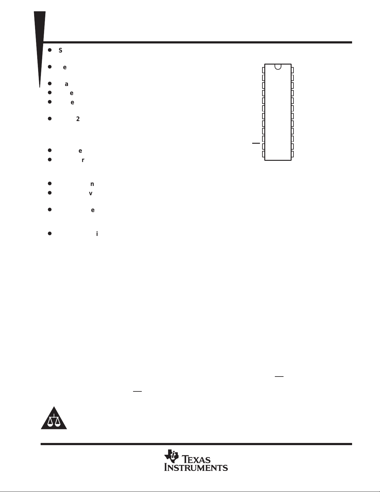
DB, DW, NT, OR PW PACKAGE
MODE
NC – No internal connection
V
DD
RA1
RA2
RA3
DY1
DY2
RA4
DY3
RA5
V
SS
EN
(TOP VIEW)
1
24
2
23
3
22
4
21
5
20
6
19
7
18
8
17
9
16
10
15
11
14
12
13
V
CC
RY1
RY2
RY3
DA1
DA2
RY4
DA3
RY5
GND
NC
NC
description
The SN75LPE185 is a low-power bipolar device containing three drivers and five receivers, with 15-kV ESD
protection on the bus pins, with respect to each other. Bus pins are defined as those pins that tie directly to the
serial-port connector, including GND. The pinout matches the flow-through design of the industry-standard
SN75185, SN75C185, and SN75LP185, with the addition of four pins for control signals. The flow-through
pinout of the device allows easy interconnection of the UART and serial-port connector of the IBM PC
compatibles. The SN75LPE185 provides a rugged, low-cost solution for this function with the combination of
bipolar processing and 15-kV ESD protection.
The SN75LPE185 has an internal slew-rate control to provide a maximum rate of change in the output signal
of 30 V/µs. The driver output swing is clamped at ±6 V to enable the higher data rates associated with this device
and reduce EMI emissions. Although the driver outputs are clamped, the outputs can handle voltages up to
±15 V without damage.
The device has flexible control options for power management when the serial port is inactive. A common
disable for all of the drivers and receivers is provided with the active-low enable (EN
(MODE) input selects between the ST ANDBY and W AKE-UP modes. With a low-level input on the MODE pin
and a high-level input on the EN
Please be aware that an important notice concerning availability, standard warranty, and use in critical applications of
Texas Instruments semiconductor products and disclaimers thereto appears at the end of this data sheet.
IBM and PC are trademarks of International Business Machines Corporation.
PRODUCTION DATA information is current as of publication date.
Products conform to specifications per the terms of Texas Instruments
standard warranty. Production processing does not necessarily include
testing of all parameters.
pin, one receiver remains active while the remaining drivers and receivers are
Copyright 1998, Texas Instruments Incorporated
) input. The mode control
POST OFFICE BOX 655303 • DALLAS, TEXAS 75265
1
Page 2
SN75LPE185
LOW-POWER MULTIPLE RS-232 DRIVERS/RECEIVERS
WITH ENABLE
SLLS256D – DECEMBER 1996 – REVISED OCTOBER 1998
description (continued)
disabled to implement the WAKE-UP mode. With a high-level input on both the MODE and EN pins, all drivers
and receivers are disabled to implement the STANDBY mode. The outputs of the drivers are in a
high-impedance state when the device is powered off. To ensure the outputs of the receivers are in a known
output level (as listed in the
in ST ANDBY , or WAKE-UP mode, external pullup/pulldown circuitry must be provided. All the logic inputs accept
3.3-V or 5-V input signals.
The SN75LPE185 complies with the requirements of TIA/EIA-232-F and ITU v .28 standards. These standards
are for data interchange between a host computer and peripheral at signaling rates up to 20 kbit/s. The switching
speeds of the SN75LPE185 support rates up to 256 kbit/s.
The SN75LPE185 is characterized for operation from 0°C to 70°C.
Application Information
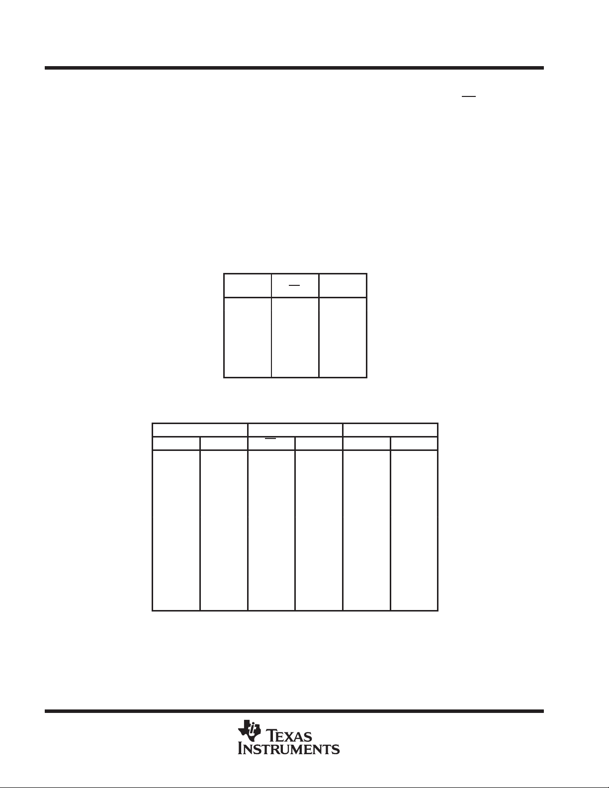
Function Tables
DRIVERS
INPUT
DA
X H Z
H L L
L L H
Open L L
H Open L
L Open H
H = high level, L = low level,
X = irrelevant, Z = high impedance (off)
ENABLEENOUTPUT
section of this data sheet) when the device is powered off,
DY
RECEIVERS
INPUTS
RA1–RA4 RA5 EN MODE RY1–RY4 RY5
H H L X L L
L L L X H H
X H H L Z L
X L H L Z H
X X H H Z Z
Open Open L X H H
H H L Open L L
L L L Open H H
X H H Open Z L
X L H Open Z H
H H Open X L L
L L Open X H H
H = high level, L = low level, X = irrelevant, Z = high impedance (off)
ENABLE INPUTS OUTPUTS
2
POST OFFICE BOX 655303 • DALLAS, TEXAS 75265
Page 3
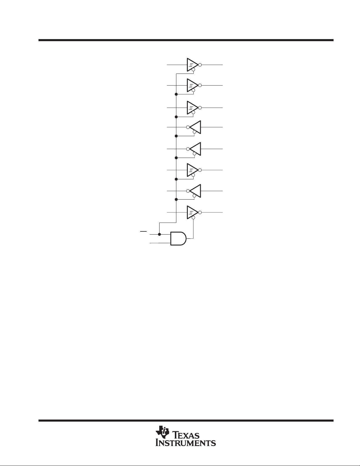
functional logic diagram (positive logic)
SN75LPE185
LOW-POWER MULTIPLE RS-232 DRIVERS/RECEIVERS
WITH ENABLE
SLLS256D – DECEMBER 1996 – REVISED OCTOBER 1998
EN
MODE
2
RA1 RY1
3
RA2
4
RA3
5
DY1
6
DY2
7
RA4
8
DY3
9
RA5
11
12
23
22
21
20
19
18
17
16
RY2
RY3
DA1
DA2
RY4
DA3
RY5
POST OFFICE BOX 655303 • DALLAS, TEXAS 75265
3
Page 4
SN75LPE185
LOW-POWER MULTIPLE RS-232 DRIVERS/RECEIVERS
WITH ENABLE
SLLS256D – DECEMBER 1996 – REVISED OCTOBER 1998
absolute maximum ratings over operating free-air temperature range (unless otherwise noted)
Positive supply voltage range:V
Negative supply voltage range, V
Receiver input voltage range, V
Driver input voltage range, V
Receiver output voltage range, V
Driver output voltage range, V
Electrostatic discharge, bus pins: Machine model (see Note 2) Class 3, 500 V. . . . . . . . . . . . . . . . . . . . . . . . . .
Electrostatic discharge, all pins: Human-body model (see Note 2) Class 3, 5 kV. . . . . . . . . . . . . . . . . . . . . . .
Package thermal impedance, θ
Storage temperature range, T
Lead temperature 1,6 mm (1/16 inch) from case for 10 seconds 260°C. . . . . . . . . . . . . . . . . . . . . . . . . . . . . . .
†
Stresses beyond those listed under “absolute maximum ratings” may cause permanent damage to the device. These are stress ratings only, and
functional operation of the device at these or any other conditions beyond those indicated under “recommended operating conditions” is not
implied. Exposure to absolute-maximum-rated conditions for extended periods may affect device reliability.
NOTES: 1. All voltage values are with respect to network ground terminal unless otherwise noted.
2. Per MIL-STD-883 Method 3015.7
3. The package thermal impedance is calculated in accordance with JESD 51, except for through-hole packages, which use a trace
length of zero.
(see Note 1) –0.5 V to 7 V. . . . . . . . . . . . . . . . . . . . . . . . . . . . . . . . . . . . . . .
CC
(see Note 1) –0.5 V to 15 V. . . . . . . . . . . . . . . . . . . . . . . . . . . . . . . . . . . . . .
V
DD
(see Note 1) 0.5 V to –15 V. . . . . . . . . . . . . . . . . . . . . . . . . . . . . . . . . . . . .
SS
(RA) –30 V to 30 V. . . . . . . . . . . . . . . . . . . . . . . . . . . . . . . . . . . . . . . . . . . . . . . . .
I
(DA, EN, MODE) –0.5 V to V
I
(RY) –0.5 V to 6 V. . . . . . . . . . . . . . . . . . . . . . . . . . . . . . . . . . . . . . . . . . . . . .
O
(DY) –15 V to 15 V. . . . . . . . . . . . . . . . . . . . . . . . . . . . . . . . . . . . . . . . . . . . . . . . .
O
Human-body model (see Note 2) Class 3, 15 kV. . . . . . . . . . . . . . . . . . . . . .
IEC1000-4-2: contact Class 3, 8 kV. . . . . . . . . . . . . . . . . . . . . . . . . . . . . . . . .
IEC1000-4-2: airgap Class 3, 15 kV. . . . . . . . . . . . . . . . . . . . . . . . . . . . . . . . .
Machine model (see Note 2) Class 3, 200 V. . . . . . . . . . . . . . . . . . . . . . . . . .
(see Note 3): DB package 104°C/W. . . . . . . . . . . . . . . . . . . . . . . . . . . . . . . . .
JA
DW package 81°C/W. . . . . . . . . . . . . . . . . . . . . . . . . . . . . . . . .
NT package 67°C/W. . . . . . . . . . . . . . . . . . . . . . . . . . . . . . . . . .
PW package 120°C/W. . . . . . . . . . . . . . . . . . . . . . . . . . . . . . . .
–65°C to 150°C. . . . . . . . . . . . . . . . . . . . . . . . . . . . . . . . . . . . . . . . . . . . . . . . . . .
stg
CC
+ 0.4 V. . . . . . . . . . . . . . . . . . . . . . . . . . . . . . . . .
†
recommended operating conditions
MIN NOM MAX UNIT
Supply voltage, VCC (see Note 4) 4.75 5 5.25 V
Supply voltage, V
Supply voltage, V
High level input voltage, V
Low level input voltage, V
Receiver input voltage range, V
High level output current, I
Low level output current, I
Operating free air temperature, T
NOTE 4: VCC cannot be greater than VDD.
DD
SS
IH
IL
I
OH
OL
A
DA, EN, MODE 2 V
DA, EN, MODE 0.8 V
RA –25 25 V
RY –1 mA
RY 2 mA
9 12 15 V
–9 –12 –15 V
0 70 °C
4
POST OFFICE BOX 655303 • DALLAS, TEXAS 75265
Page 5

µ
CC
y
CC
minimum V
µ
or maximum V
OL
µ
DD
y
DD
minimum V
µ
or maximum V
OL
SS
y
SS
minimum V
OH
µ
OL
V
g
I
,
L
,
V
V
I
,
L
,
V
SN75LPE185
LOW-POWER MULTIPLE RS-232 DRIVERS/RECEIVERS
WITH ENABLE
SLLS256D – DECEMBER 1996 – REVISED OCTOBER 1998
supply currents over the recommended operating conditions (unless otherwise noted)
PARAMETER TEST CONDITIONS
VDD = 9 V, VSS = –9 V, EN at GND,
No load,
SS
All inputs at
or maximum V
No load,
All inputs at
or maximum V
No load,
All inputs at
or maximum V
OH
OH
I
I
I
SS
NOTE 5: Minimum RS-232 driver output voltages are not attained with ±5-V supplies.
Supply current for V
Supply current for V
Supply current for V
See Note 5
VDD = 12 V, VSS = –12 V, EN at GND 1000
EN, MODE at V
EN at VCC, MODE at GND 700
VDD = 9 V, VSS = –9 V, EN at GND,
See Note 5
VDD = 12 V, VSS = –12 V, EN at GND 800
EN, MODE at V
EN at VCC, MODE at GND 20
VDD = 9 V, VSS = –9 V, EN at GND,
See Note 5
VDD = 12 V, VSS = –12 V, EN at GND
EN, MODE at V
EN at VCC, MODE at GND –50
CC
CC
CC
MIN TYP MAX UNIT
1000
650
800
20
–625
–625
–50
A
A
µA
driver electrical characteristics over the recommended operating conditions (unless otherwise
noted)
PARAMETER TEST CONDITIONS
VDD = 9 V, VSS = –9 V, EN at GND,
OH
OL
I
IH
I
IL
I
OZ
I
OS(H)
I
OS(L)
r
o
NOTES: 5. Minimum RS-232 driver output voltages are not attained with ±5-V supplies.
High-level V
output voltage
Low-level V
output voltage
High-level input current VI at V
Low-level input current VI at GND –1 µA
High-impedance
output current
Short-circuit high-level
output current
Short-circuit low-level
output current
Output resistance VDD = VSS = VCC = 0, VO = 2 V 300 Ω
6. Maximum output swing is limited to ±5.5 V to enable the higher data rates associated with this device and to reduce EMI emissions.
7. Not more than one output should be shorted at one time.
= 0.8 V, R
See Figure 1
= 2 V, R
See Figure 1
VCC = 5 V,
VO = GND or VSS, See Figure 2 and Note 7 –30 –55 mA
VO = GND or VSS, See Figure 2 and Note 7 30 55 mA
= 3 kΩ,
= 3 K,
CC
See Note 5
VDD = 12 V, VSS = –12 V,
EN
at GND, See Note 6
VDD = 9 V, VSS = –9 V, EN at GND,
See Note 5
VDD = 12 V, VSS = –12 V,
EN
at GND, See Note 6
VDD = 12 V, VSS = –12 V,
–5 V ≤ VO ≤ 5 V
MIN TYP MAX UNIT
5 5.8 6.6
5 5.8 6.6
–5 –5.8 –6.9
–5 –5.8 –6.9
1 µA
±100 µA
POST OFFICE BOX 655303 • DALLAS, TEXAS 75265
5
Page 6

SN75LPE185
R
C
See Figure 1
ns
L
,
,
s
L
,
,
s
t
,
V
ns
t
,
V
ns
LOW-POWER MULTIPLE RS-232 DRIVERS/RECEIVERS
WITH ENABLE
SLLS256D – DECEMBER 1996 – REVISED OCTOBER 1998
driver switching characteristics over operating free-air temperature range (unless otherwise
noted)
PARAMETER TEST CONDITIONS
t
PHL
t
PLH
t
PZL
t
PZH
t
PLZ
t
PHZ
TLH
THL
SR Output slew rate
NOTE 6: Maximum output swing is limited to ±5.5 V to enable the higher data rates associated with this device and to reduce EMI emissions.
Propagation delay time,
high-to low-level output
Propagation delay time,
low-to high-level output
Driver output-enable time
to low-level output
Driver output-enable time
to high-level output
Driver output-disable time
from low-level output
Driver output-disable time
from high-level output
Transition time,
low-to high-level output
Transition time,
high-to low-level output
= 3 kΩ to 7 kΩ,
L
R
= 3 kΩ to 7 kΩ, STANDBY or WAKE-UP modes,
CL = 15 pF
R
= 3 kΩ to 7 kΩ, STANDBY or WAKE-UP modes,
CL = 15 pF
VCC = 5 V,
VDD = 12 V,
= –12 V,
SS
RL = 3 kΩ to 7 kΩ,
See Figure 1 and Note 6
VCC = 5 V,
VDD = 12 V,
= –12 V,
SS
RL = 3 kΩ to 7 kΩ
See Figure 1 and Note 6
VCC = 5 V,
VDD = 12 V,
VSS = –12 V,
RL = 3 kΩ to 7 kΩ,
CL = 15 pF,
See Note 6
See Figures 1, 6, and Note 6
See Figures 1, 6, and Note 6
Using 10%-to-90% transition region,
Driver speed = 250 kbit/s
CL = 15 pF
Using ±3-V transition region,
Driver speed = 250 kbit/s
CL = 15 pF
Using ±2-V transition region,
Driver speed = 250 kbit/s
CL = 15 pF
Using ±3-V transition region,
Driver speed = 125 kbit/s
CL = 2500 pF
Using 10%-to-90% transition region,
Driver speed = 250 kbit/s
CL = 15 pF
Using ±3-V transition region,
Driver speed = 250 kbit/s
CL = 15 pF
Using ±2-V transition region,
Driver speed = 250 kbit/s
CL = 15 pF
Using ±3-V transition region,
Driver speed = 125 kbit/s
CL = 2500 pF
Using ±3-V transition region,
Driver speed = 0 to 250 kbit/s
= 15 pF,
L
p
MIN TYP MAX UNIT
300 800 1600
300 800 1600
50 100
µ
50 100
50 100
µ
50 100
375 2240
200 1500
133 1000
2750
375 2240
200 1500
133 1000
2750
4 20 30 V/µs
6
POST OFFICE BOX 655303 • DALLAS, TEXAS 75265
Page 7

IIHHigh-level input current
mA
IILLow-level input current
mA
ns
ns
STANDBY mode
s
s
ns
SN75LPE185
LOW-POWER MULTIPLE RS-232 DRIVERS/RECEIVERS
WITH ENABLE
SLLS256D – DECEMBER 1996 – REVISED OCTOBER 1998
receiver electrical characteristics over recommended operating free-air temperature range
(unless otherwise noted)
PARAMETER TEST CONDITIONS
V
IT+
V
IT–
V
HYS
V
OH
V
OL
I
OS(H)
I
OS(L)
I
OZ
R
IN
NOTE 7: Not more than one output should be shorted at one time.
Positive-going input threshold voltage See Figure 3 1.6 2 2.55 V
Negative-going input threshold voltage See Figure 3 0.6 1 1.45 V
Input hysteresis, V
High-level output voltage IOH = –1 mA, 2.5 3.9 V
Low-level output voltage IOL = 2 mA, 0.33 0.5 V
p
p
Short-circuit high-level output current VO = 0, See Figure 5 and Note 7 –20 mA
Short-circuit low-level output current VO = VCC, See Figure 5 and Note 7 20 mA
High-impedance output current VCC= 0 or 5 V, 0.3 V ≤ VO ≤ V
Input resistance VI = ±3 V to ±25 V 3 5 7 kΩ
IT+
– V
IT–
See Figure 3 600 1100 mV
VI = 3 V 0.43 0.6 1
VI = 25 V 3.6 5.1 8.3
VI = –3 V –0.43 –0.6 –1
VI = –25 V –3.6 –5.1 –8.3
CC
MIN TYP MAX UNIT
±100 µA
receiver switching characteristics over recommended operating free-air temperature range
(unless otherwise noted)
t
PHL
t
PLH
t
TLH
t
THL
t
SK(P)
t
PZL
t
PZH
t
PLZ
t
PHZ
t
PHL
t
PLH
PARAMETER TEST CONDITIONS
Propagation delay time, high- to low-level output 400 900
Propagation delay time, low- to high-level output 400 900
Transition time low- to high-level output 200 500
Transition time high- to low-level output 200 400
Pulse skew |t
Receiver output-enable time to low-level output
Receiver output-enable time to high-level output
Receiver output-disable time from low-level output 50 100
Receiver output-disable time from high-level output 50 100
Propagation delay time, high- to low-level output (WAKE-UP mode) 500 1500
Propagation delay time, low- to high-level output (WAKE-UP mode) 500 1500
PLH
– t
PHL
|
STANDBY mode
CL = 50 pF,
See Figures 4 and 7
MIN TYP MAX UNIT
200 425 ns
50 100
50 100
µ
µ
POST OFFICE BOX 655303 • DALLAS, TEXAS 75265
7
Page 8

SN75LPE185
LOW-POWER MULTIPLE RS-232 DRIVERS/RECEIVERS
WITH ENABLE
SLLS256D – DECEMBER 1996 – REVISED OCTOBER 1998
PARAMETER MEASUREMENT INFORMATION
Inputs Outputs
I
I
V
I
V
I
O
O
C
L
R
L
V
I
t
PLH
V
O
50% 50%
50%
V
TR–
t
TLH
t
w
V
TR+VTR+
t
50%
V
PHL
TR–
t
THL
3 V
0 V
V
V
OH
OL
NOTES: A. The pulse generator has the following characteristics:
For CL < 1000 pF: tw = 4 µs, PRR = 250 kbit/s, ZO = 50 Ω, tr = tf < 50 ns.
For CL = 2500 pF: tw = 8 µs, PRR = 125 kbit/s, ZO = 50 Ω, tr = tf < 50 ns.
B. CL includes probe and jig capacitance.
Figure 1. Driver Parameter Test Circuit and Waveform
Inputs Outputs
I
I
V
I
V
O
Figure 2. Driver IOS Test
Inputs Outputs
I
I
V
I
V
V
DD
V
GND
SS
CC
I
O
I
O
V
O
Figure 3. Receiver VIT Test
t
w
Inputs Outputs
I
I
V
I
NOTES: A. The pulse generator has the following characteristics: tw = 4 µs, PRR = 250 kbit/s, ZO = 50 Ω, tr = tf < 50 ns.
B. CL includes probe and jig capacitance.
V
I
O
C
L
O
V
I
t
PLH
V
O
50% 50%
50%
10% 10%
t
TLH
90% 90%
t
50%
Figure 4. Receiver Parameter Test Circuit and Waveform
8
POST OFFICE BOX 655303 • DALLAS, TEXAS 75265
PHL
t
THL
V
IH
V
IL
V
OH
V
OL
Page 9

SN75LPE185
LOW-POWER MULTIPLE RS-232 DRIVERS/RECEIVERS
WITH ENABLE
SLLS256D – DECEMBER 1996 – REVISED OCTOBER 1998
PARAMETER MEASUREMENT INFORMATION
Inputs Outputs
From Output
Under Test
CL = 15 pF
(see Note A)
LOAD CIRCUIT
I
I
V
I
V
I
O
O
V
GND
CC
Figure 5. Receiver IOS Test
3 V
V
R
L
Waveform 1
(see Note B)
Waveform 2
(see Note B)
I
t
PZL
V
O
t
PZH
V
O
VOLTAGE WAVEFORMS
ENABLE AND DISABLE TIMES
t
PLZ
50%
t
PHZ
50%
50%50%
VOL + 0.3 V
VOH – 0.3 V
0 V
0 V
V
V
0 V
OL
OH
NOTES: A. CL includes probe and jig capacitance.
B. Waveform 1 is for an output with internal conditions such that the output is low except when disabled by the output control.
Waveform 2 is for an output with internal conditions such that the output is high except when disabled by the output control.
C. All input pulses are supplied by generators having the following characteristics: PRR = 250 kbit/s, ZO = 50 Ω, tr = tf < 50 ns.
D. The outputs are measured one at a time with one transition per measurement.
Figure 6. Driver 3-State Parameter Circuit and Voltage Waveforms
POST OFFICE BOX 655303 • DALLAS, TEXAS 75265
9
Page 10

SN75LPE185
LOW-POWER MULTIPLE RS-232 DRIVERS/RECEIVERS
WITH ENABLE
SLLS256D – DECEMBER 1996 – REVISED OCTOBER 1998
PARAMETER MEASUREMENT INFORMATION
4 V
From Output
Under Test
CL = 50 pF
(see Note A)
5k Ω
LOAD CIRCUIT
V
I
t
PZL
S1
Open
GND
t
PLZ
50%50%
TEST S1
t
PHL/tPLH
t
PLZ/tPZL
t
PHZ/tPZH
3 V
0 V
Open
4 V
GND
V
Waveform 1
(see Note B)
Waveform 2
(see Note B)
NOTES: A. CL includes probe and jig capacitance.
B. Waveform 1 is for an output with internal conditions such that the output is low except when disabled by the output control.
Waveform 2 is for an output with internal conditions such that the output is high except when disabled by the output control.
C. All input pulses are supplied by generators having the following characteristics: PRR = 250 kbit/s, ZO = 50 Ω, tr = tf < 50 ns.
D. The outputs are measured one at a time with one transition per measurement.
O
t
V
O
Figure 7. Receiver 3-State Parameter Test Circuit and Voltage Waveforms
50%
t
PZH
VOLTAGE WAVEFORMS
ENABLE AND DISABLE TIMES
PHZ
50%
VOL + 0.3 V
VOH – 0.3 V
4 V
V
V
0 V
OL
OH
10
POST OFFICE BOX 655303 • DALLAS, TEXAS 75265
Page 11

receiver output states
SN75LPE185
LOW-POWER MULTIPLE RS-232 DRIVERS/RECEIVERS
WITH ENABLE
SLLS256D – DECEMBER 1996 – REVISED OCTOBER 1998
APPLICATION INFORMATION
DURING POWER-DOWN, STANDBY, OR WAKE-UP MODES
RECEIVER NUMBER SIGNAL NAME RECEIVER OUTPUT
RECEIVER KNOWN OUTPUT STATES
RY1 DCD HIGH
RY2 DSR HIGH
RY3 RX LOW
RY4 CTS HIGH
RY5 RI HIGH
fault protection during power down
Diodes placed in series with the VDD and VSS leads protect the SN75LPE185 in the fault condition, in which the device
outputs are shorted to ±15 V and the power supplies are at low voltage and provide low-impedance paths to ground.
V
DD
SN75LPE185Output SN75LPE185Output
V
SS
Figure 8. Power-Supply Protection to Meet Power-Off Fault Conditions of TIA/EIA-232-F
POST OFFICE BOX 655303 • DALLAS, TEXAS 75265
11
Page 12

SN75LPE185
LOW-POWER MULTIPLE RS-232 DRIVERS/RECEIVERS
WITH ENABLE
SLLS256D – DECEMBER 1996 – REVISED OCTOBER 1998
APPLICATION INFORMATION
WAKE-UP mode
While in the WAKE-UP mode, all the drivers and receivers of the SN75LPE185 device are in the high-impedance
state, except for receiver 5, which can be used as a Ring Indicator function. In this mode, the current drawn from
the power supplies is low, to conserve power.
In today’s PCs, board designers are becoming more concerned about power consumption. The flexibility of the
SN75LPE185 during WAKE-UP mode allows the designer to operate the device at auxiliary power-supply
voltages below specified levels. The SN75LPE185 functions properly during WAKE-UP mode, using the
following power-supply conditions:
(a) V
(b) V
(c) V
(d) V
Condition (a) describes the minimum supply voltages necessary for the device to comply fully to specifications.
Conditions (b) and (d) describe the condition where a –5-V supply is not available during auxiliary power. In this
case, V
Condition (c) states V
In all cases, GND is understood to be 0 V, and the power supply voltages should never exceed the absolute
maximum ratings.
must be shorted to the most negative supply (i.e., GND or a voltage source close to, but below GND).
SS
= 4.75 V, VDD = 9 V, and VSS = –9 V (data-sheet specifications)
CC
= 5 V, VDD = 5 V, and VSS = –5 V
CC
= 5 V, VDD = open, and VSS = open
CC
= 5 V, VDD = 5 V, and VSS is shorted to the most negative supply.
CC
and VSS power supplies can be shut off.
DD
12
POST OFFICE BOX 655303 • DALLAS, TEXAS 75265
Page 13

IMPORTANT NOTICE
T exas Instruments and its subsidiaries (TI) reserve the right to make changes to their products or to discontinue
any product or service without notice, and advise customers to obtain the latest version of relevant information
to verify, before placing orders, that information being relied on is current and complete. All products are sold
subject to the terms and conditions of sale supplied at the time of order acknowledgement, including those
pertaining to warranty, patent infringement, and limitation of liability.
TI warrants performance of its semiconductor products to the specifications applicable at the time of sale in
accordance with TI’s standard warranty. Testing and other quality control techniques are utilized to the extent
TI deems necessary to support this warranty . Specific testing of all parameters of each device is not necessarily
performed, except those mandated by government requirements.
CERT AIN APPLICATIONS USING SEMICONDUCTOR PRODUCTS MAY INVOLVE POTENTIAL RISKS OF
DEATH, PERSONAL INJURY, OR SEVERE PROPERTY OR ENVIRONMENTAL DAMAGE (“CRITICAL
APPLICATIONS”). TI SEMICONDUCTOR PRODUCTS ARE NOT DESIGNED, AUTHORIZED, OR
WARRANTED TO BE SUITABLE FOR USE IN LIFE-SUPPORT DEVICES OR SYSTEMS OR OTHER
CRITICAL APPLICA TIONS. INCLUSION OF TI PRODUCTS IN SUCH APPLICATIONS IS UNDERST OOD TO
BE FULLY AT THE CUSTOMER’S RISK.
In order to minimize risks associated with the customer’s applications, adequate design and operating
safeguards must be provided by the customer to minimize inherent or procedural hazards.
TI assumes no liability for applications assistance or customer product design. TI does not warrant or represent
that any license, either express or implied, is granted under any patent right, copyright, mask work right, or other
intellectual property right of TI covering or relating to any combination, machine, or process in which such
semiconductor products or services might be or are used. TI’s publication of information regarding any third
party’s products or services does not constitute TI’s approval, warranty or endorsement thereof.
Copyright 1998, Texas Instruments Incorporated
 Loading...