

Page 1
HHLHLLHHHHH
SN75LBC786
QUADRUPLE RS-423-B DRIVER/RECEIVER WITH LOOPBACK
SLLS184 – NOVEMBER 1994
D
Four Independent Drivers and Receivers
D
Loopback Mode Functionally Self Tests
Drivers and Receivers Without
Disconnection From Line
D
Driver Slew Rate Controlled by a Single
Resistor
D
Internal Thermal-Overload Protection
D
RS-423-B Inputs and Outputs Designed to
Withstand ±25 V
D
ESD Protection Exceeds 2000 V Per
MIL-STD-833C Method 3015
D
LinBiCMOS Process Technology
description
The SN75LBC786 is a monolithic quadruple
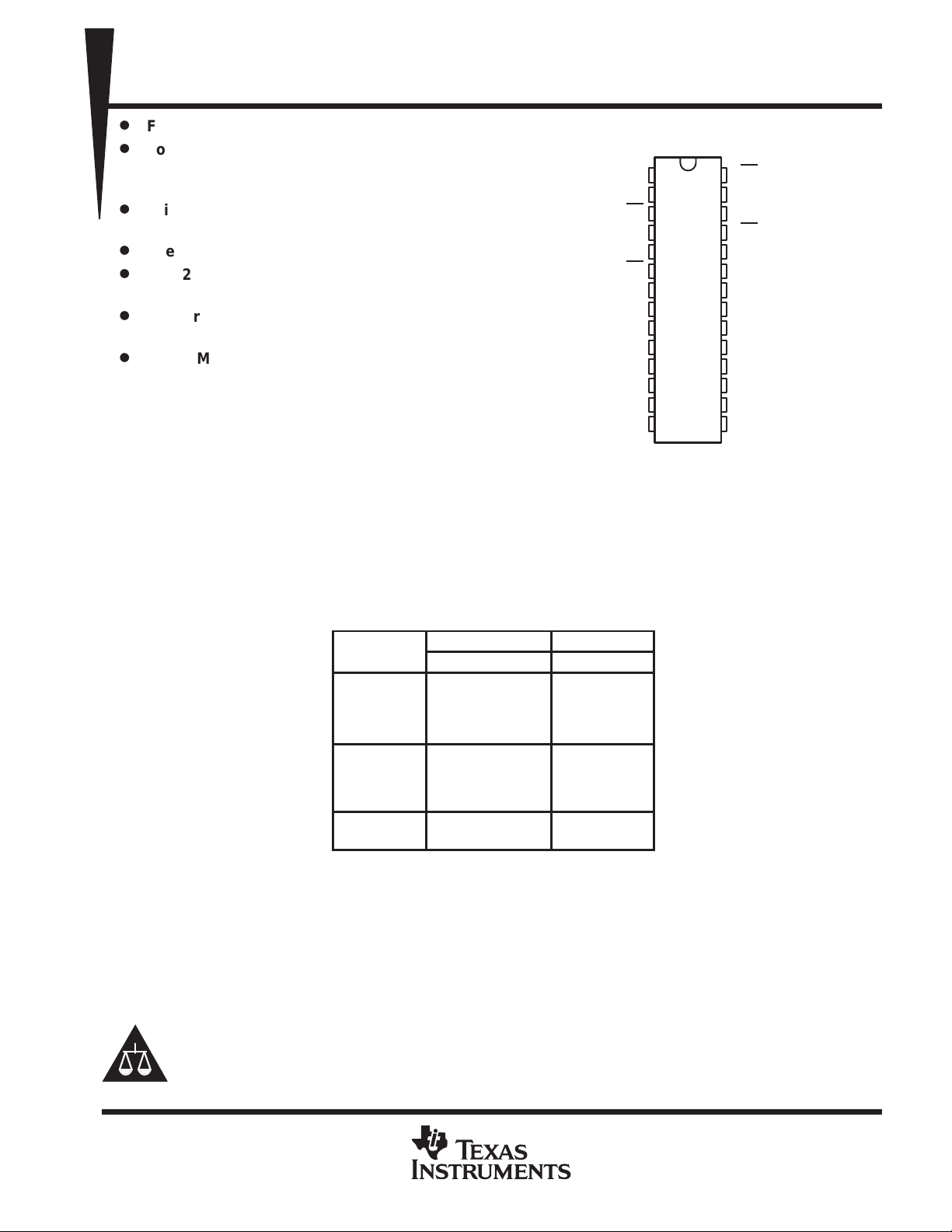
DW PACKAGE
3A
3Z
3LB
4A
4Z
4LB
V
SS
GND
4B
4Y
3B
3Y
3C
4C
(TOP VIEW)
1
28
2
27
3
26
4
25
5
24
6
23
7
22
8
21
9
20
10
19
11
18
12
17
13
16
14
15
2LB
2Z
2A
1LB
1Z
1A
R
WS
V
DD
1Y
1B
2Y
2B
2C
1C
RS-423-B driver and receiver with integratedloopback function. The operation of the
SN75LBC786 is closely based on that of the SN75186. In normal operation, the device performs as four
independent RS-423-B driver/receiver pairs designed to interface data-terminal equipment (DTE) with data
circuit-terminating equipment (DCE). In loopback mode, the signal from each driver output is fed back via
special circuitry into its associated receiver input, removing the need to locally disconnect cables and install a
loopback connector. The receiver output signal is the same as the driver input signal.
The SN75LBC786 is characterized for operation over the temperature range of 0°C to 70°C.
FUNCTION TABLE
LOOPBACK
LB
H L HL L H
H H HL L L
H
H
H
H
L
L
H = high level, L = low level, X = irrelevant, ? = indeterminate
INPUTS OUTPUTS
A B C Z Y
L
L
L
H
L
H
L
H
L
H
H
X
X
L
H
H
X
X
?
?
?
?
L
H
L
H
L
H
L
L
L
Please be aware that an important notice concerning availability, standard warranty, and use in critical applications of
Texas Instruments semiconductor products and disclaimers thereto appears at the end of this data sheet.
LinBiCMOS is a trademark of Texas Instruments Incorporated.
PRODUCTION DATA information is current as of publication date.
Products conform to specifications per the terms of Texas Instruments
standard warranty. Production processing does not necessarily include
testing of all parameters.
POST OFFICE BOX 655303 • DALLAS, TEXAS 75265
Copyright 1994, T exas Instruments Incorporated
1
Page 2
SN75LBC786
QUADRUPLE RS-423-B DRIVER/RECEIVER WITH LOOPBACK
SLLS184 – NOVEMBER 1994
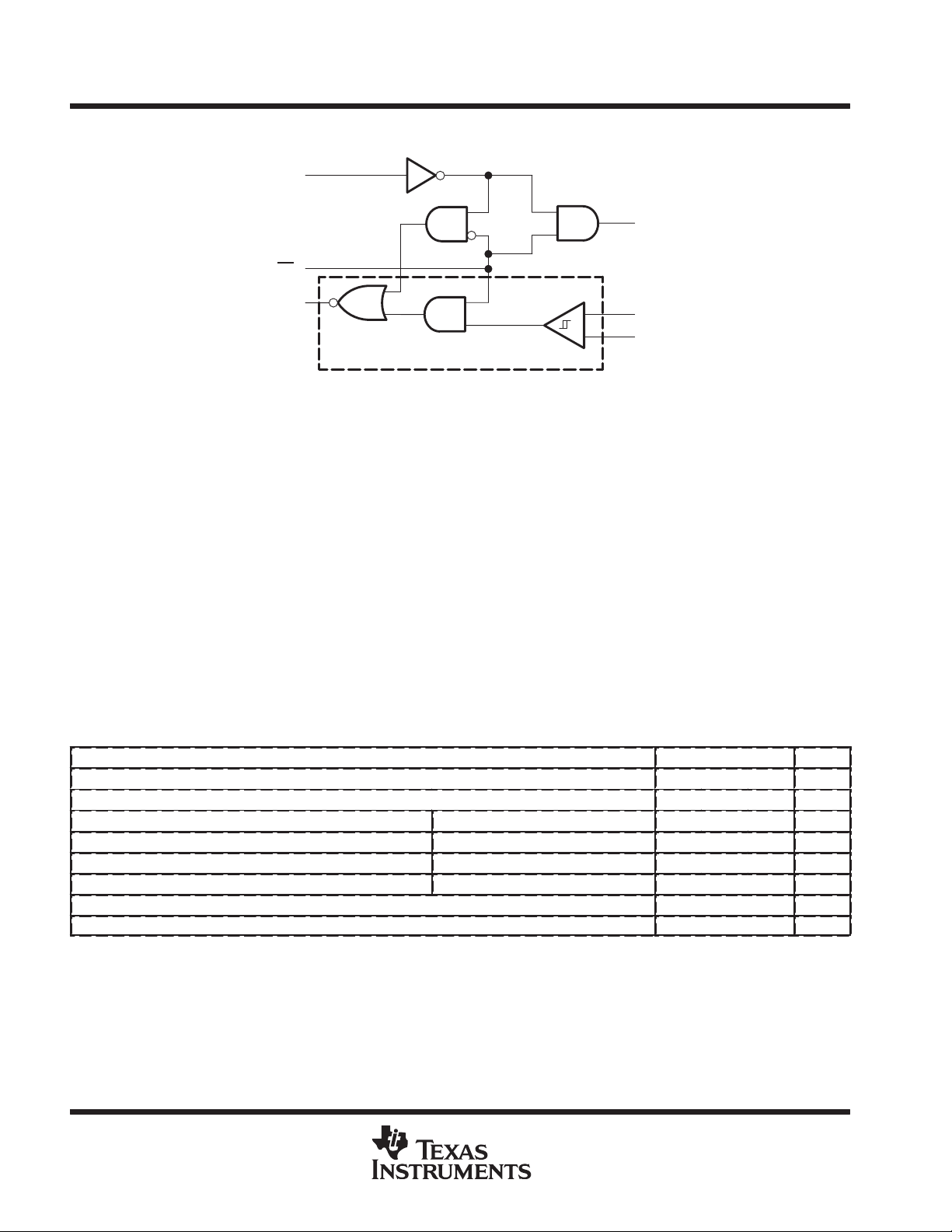
logic diagram (positive logic) (each transceiver)
Driver
A
LB
Y
Z
Receiver
–
+
C
B
absolute maximum ratings over operating free-air temperature range (unless otherwise noted)
Positive supply voltage, V
Negative supply voltage, V
Receiver input voltage range –30 V to 30 V. . . . . . . . . . . . . . . . . . . . . . . . . . . . . . . . . . . . . . . . . . . . . . . . . . . . . . . .
Driver input voltage range –0.5 V to 5.75 V. . . . . . . . . . . . . . . . . . . . . . . . . . . . . . . . . . . . . . . . . . . . . . . . . . . . . . . .
Loopback input voltage range –0.5 V to 5.75 V. . . . . . . . . . . . . . . . . . . . . . . . . . . . . . . . . . . . . . . . . . . . . . . . . . . .
Driver output voltage range (supplies at 0 V) –30 V to 30 V. . . . . . . . . . . . . . . . . . . . . . . . . . . . . . . . . . . . . . . . . .
Driver output voltage range (supplies at ±12 V) –25 V to 25 V. . . . . . . . . . . . . . . . . . . . . . . . . . . . . . . . . . . . . . . .
Continuous power dissipation at (or below) T
Operating free-air temperature range, T
Storage temperature range, T
Case temperature for 10 seconds 260°C. . . . . . . . . . . . . . . . . . . . . . . . . . . . . . . . . . . . . . . . . . . . . . . . . . . . . . . . . .
†
Stresses beyond those listed under “absolute maximum ratings” may cause permanent damage to the device. These are stress ratings only, and
functional operation of the device at these or any other conditions beyond those indicated under “recommended operating conditions” is not
implied. Exposure to absolute-maximum-rated conditions for extended periods may affect device reliability.
NOTE 1: All voltages are with respect to network ground terminal.
(see Note 1) 14 V. . . . . . . . . . . . . . . . . . . . . . . . . . . . . . . . . . . . . . . . . . . . . . . . . . . . .
DD
–14 V. . . . . . . . . . . . . . . . . . . . . . . . . . . . . . . . . . . . . . . . . . . . . . . . . . . . . . . . . . . . . . .
SS
= 70°C 800 mW. . . . . . . . . . . . . . . . . . . . . . . . . . . . . . . . . . . . . . . .
A
0°C to 70°C. . . . . . . . . . . . . . . . . . . . . . . . . . . . . . . . . . . . . . . . . . . . . .
–65°C to 150°C. . . . . . . . . . . . . . . . . . . . . . . . . . . . . . . . . . . . . . . . . . . . . . . . . . .
stg
A
recommended operating conditions
MIN NOM MAX UNIT
Supply voltage, V
Supply voltage, V
High-level input voltage, V
Low-level input voltage, V
High-level output current, I
Low-level output current, I
Slew rate control resistor, R
Operating free-air temperature, T
DD
SS
IH
IL
OH
OL
WS
Driver and loopback 2 V
Driver and loopback 0.8 V
Receiver –4 mA
Receiver 4 mA
A
10.8 12 13.2 V
–10.8 –12 –13.2 V
20 82 820 kΩ
0 70 °C
†
2
POST OFFICE BOX 655303 • DALLAS, TEXAS 75265
Page 3
IDDSupply current (loopback off)
mA
ISSSupply current (loopback off)
mA
s
(see Figure 1)
L
s
(see Figure 1)
SN75LBC786
QUADRUPLE RS-423-B DRIVER/RECEIVER WITH LOOPBACK
SLLS184 – NOVEMBER 1994
DRIVER SECTION
electrical characteristics over recommended ranges of supply voltage and operating free-air
temperature (unless otherwise noted)
PARAMETER TEST CONDITIONS MIN TYP MAX UNIT
V
OH
V
OL
I
IH
I
IL
I
IKG
I
OS(H)
I
OS(L)
I
DD(LB)
I
DD
LOOPBACK MODE
High-level output voltage Open circuit or RI = 450 Ω 4 5.5 6 V
Low-level output voltage Open circuit or RI = 450 Ω –6 –5.5 –4 V
High-level input current VI = 2.4 V – 5.5 V 100 µA
Low-level input current VI = 0 V – 0.8 V –100 µA
Output leakage current VDD = VSS = 0 V, VO = ±6 V –100 100 µA
High-level short-circuit output current VI = high, VO = 0 V 15 45 mA
Low-level short-circuit output current VI = low, VO = 0 V –45 –15 mA
pp
Supply current with loopback on No load, LB at 0.8 V 13 16 mA
pp
Supply current with loopback on No load, LB at 0.8 V –13 –16 mA
Output voltage (input either high or low) RI = >450 Ω, VLB = low –6 –5.5 –4 V
p
p
No load, LB at 2 V 10 12
RI = 450 Ω, LB at 2 V 60 70
No load, LB at 2 V –10 –12
RI = 450 Ω, LB at 2 V –60 –70
switching characteristics over recommended ranges of supply voltage and operating free-air
temperature (unless otherwise noted)
PARAMETER TEST CONDITIONS MIN TYP MAX UNIT
RWS = 0 kΩ 1.5
Transition time, low-to-high level output
t
TLH
RI = 450 Ω, CL = 50 pF,
VWS = 5 V
Transition time, high-to-low level output
t
THL
SR Output slew rate RWS = 20 kΩ 15 V/µs
t
sk
Output skew, |t
PHL
– t
| (see Figure 4) RWS = 82 kΩ 1 µs
PLH
RWS = 20 kΩ 1.5 2.1 2.7
RWS = 82 kΩ 5 8 11
RWS = 820 kΩ 80
RWS = 0 kΩ
RWS = 20 kΩ 1.5 2.1 2.7
RWS = 82 kΩ 5 8 11
RWS = 820 kΩ 80
1.5
µ
µ
POST OFFICE BOX 655303 • DALLAS, TEXAS 75265
3
Page 4

SN75LBC786
V
g
mV
IIInput current
Other input to GND
mA
VOHHigh-level output voltage (see Note 2)
V
0.15
1µs
C
pF
20
200
ns
QUADRUPLE RS-423-B DRIVER/RECEIVER WITH LOOPBACK
SLLS184 – NOVEMBER 1994
RECEIVER SECTION
electrical characteristics over recommended ranges of supply voltage and operating free-air
temperature (unless otherwise noted)
PARAMETER TEST CONDITIONS MIN TYP MAX UNIT
IT
V
hys
V
OL
I
OS
V
ID
V
ofs
NOTES: 2. Device has an internal RX supply regulator . Maximum RX logic output voltage under no load is thus defined by an internal voltage
Receiver input threshold voltage
(see Figure 5)
p
Hysteresis voltage 20 40 150 mV
p
Low-level output voltage IO = 20 µA to 4 mA 0.4 V
RX short circuit current 50 mA
Differential input voltage Receiver inputs open circuit 1.6 2.1 2.6 V
Fail safe output voltage See Note 3 3.5 V
value. This is nominally set to 4.5 V with a tolerance of ±5%.
3. One input at ground, other input open circuit, IO = –20 µA, or both open circuit.
VIT = (VI+ – VI–) –200 200
VIT = (VI+ – VI–) with 500-Ω series resistor
VI = 10 V
VI = –10 V
IO = –20 µA 3.5 5
IO = –4 mA 2.4 5
p
–400 400
1.3 3.25
–3.25 –1.3
switching characteristics over recommended ranges of supply voltage and operating free-air
temperature (unless otherwise noted)
PARAMETER TEST CONDITIONS MIN NOM MAX UNIT
t
PLH
t
PHL
t
THL
t
TLH
Propagation delay time, low-to-high (see Figure 2)
Propagation delay time, high-to-low (see Figure 2)
Transition time, high-to-low (see Figure 3)
Transition time, low-to-high (see Figure 3)
= 50
L
p
4
POST OFFICE BOX 655303 • DALLAS, TEXAS 75265
Page 5

QUADRUPLE RS-423-B DRIVER/RECEIVER WITH LOOPBACK
PARAMETER MEASUREMENT INFORMATION
5 V
R
Input
51 Ω
GND
NOTES: A. CL includes probe and jig capacitance.
B. The input pulse is supplied by a generator having the following characteristics: tr ≤ 10 nS, tf < 10 nS, Zo = 50 Ω, PRR ≥ 5 kHz, duty
cycle = 50%, V
WS
max
V
DD
V
SS
= 3 V, V
R
L
GND
= 0 V.
min
Figure 1. Driver Transition T imes
Output
C
L
(see Notes A and B)
Input
Output
SN75LBC786
SLLS184 – NOVEMBER 1994
3 V
0 V
V
OH
V
OL
t
THL
90% 90%
10% 10%
t
TLH
V
DD
Input
GND
NOTES: A. CL includes probe and jig capacitance.
B. The input pulse is supplied by a generator having the following characteristics: tr ≤ 10 nS, tf < 10 nS, Zo = 50 Ω, PRR ≥ 5 kHz, duty
cycle = 50%, V
51 Ω
+
–
max
V
SS
GND
= 0.5 V, V
Output
C
= –0.5 V.
min
L
Figure 2. Receiver Propagation Delay Times
V
DD
Input
GND
NOTES: A. CL includes probe and jig capacitance.
B. The input pulse is supplied by a generator having the following characteristics: tr ≤ 10 nS, tf < 10 nS, Zo = 50 Ω, PRR ≥ 5 kHz, duty
cycle = 50%, V
51 Ω
max
+
–
V
SS
= 0.5 V, V
GND
min
Output
C
L
= –0.5 V.
(see Notes A and B)
Output
Input
(see Notes A and B)
Output
Input
V
OH
V
OL
t
PLH
t
TLH
50%
50%
90%
10% 10%
50%
90%
50%
t
PHL
t
THL
0.5 V
–0.5 V
Figure 3. Receiver Transition Times
POST OFFICE BOX 655303 • DALLAS, TEXAS 75265
5
Page 6

SN75LBC786
QUADRUPLE RS-423-B DRIVER/RECEIVER WITH LOOPBACK
SLLS184 – NOVEMBER 1994
PARAMETER MEASUREMENT INFORMATION
500 Ω
500 Ω
V
cm
Input A
Output Y
50% 50%
t
PLH
50% 50%
t
PHL
250 mV
250 mV
Vcm = –7 to 7 V
Figure 4. Skew Definition Times Figure 5. Input Balance Test
PRINCIPLES OF OPERATION
In normal operation, the SN75LBC786 functions as four independent drivers and receivers. The loopback mode is
disabled by maintaining a high logic level on the LB
hysteresis and resistive attenuation on the inputs. The resistive attenuation improves the input common-mode range
and also provides additional protection from ESD and over-voltage stress. The differential and common-mode input
impedance are sufficiently high to meet RS-423-B. The balance of the receiver input voltage current characteristics
and bias voltage is such that the receiver remains in the intended binary state when a differential voltage of 500 mV
is applied to the inputs through 500 Ω across the entire common-mode range (see Figure 5).
The drivers meet all RS-423-B specifications. In normal operation, the drivers have built-in current limits and thermal
overload protection. Slew-rate controlling circuitry is included into the design that is adjusted to suit the application
by means of an external resistor. The slew-rate controlling circuitry also has a default mode. If R
V externally, the transition time defaults to approximately 1.5 µs. The receiver is compatible to the RS-232 with the
use of external input resistors to meet the RS-232 input-resistance specification of 3 kΩ to 7 kΩ.
input. The receivers consist of differential comparators with
is shorted to 5
WS
T aking an individual LB
input low activates the loopback mode in the corresponding driver/receiver pair. This causes
the output from that driver to be fed back to the input of its receiver through dedicated internal-loopback circuitry . Data
from the receiver output can then be compared, by a communication system, with the data transmitted to the driver
to determine if the functional operation of the driver and receiver together is correct.
In the loopback mode, external data at the input of the receiver is ignored and the driver does not transmit data onto
the line. Extraneous data is prevented internally from being sent by the driver in the loopback mode by clamping its
output to a level below the maximum interface voltage, –5 V , or the EIA-423-B marking state. Below this marking level,
a reduced 1.5-V output amplitude is used at the driver output. This signal is detected by an on-chip loopback
comparator and fed to the input stage of the receiver to complete the loop.
Line faults external to the SN75LBC786 are detected in addition to device failures. These line faults include short
circuits to ground and to external supply voltages. The loopback mode should be entered only when the driver output
is low, that is, the marking condition. It is recommended that loopback not be entered when the driver output is in a
high state as this may cause a low-level, nondamaging oscillation at the driver output.
6
POST OFFICE BOX 655303 • DALLAS, TEXAS 75265
Page 7

IMPORTANT NOTICE
T exas Instruments and its subsidiaries (TI) reserve the right to make changes to their products or to discontinue
any product or service without notice, and advise customers to obtain the latest version of relevant information
to verify, before placing orders, that information being relied on is current and complete. All products are sold
subject to the terms and conditions of sale supplied at the time of order acknowledgement, including those
pertaining to warranty, patent infringement, and limitation of liability.
TI warrants performance of its semiconductor products to the specifications applicable at the time of sale in
accordance with TI’s standard warranty. Testing and other quality control techniques are utilized to the extent
TI deems necessary to support this warranty . Specific testing of all parameters of each device is not necessarily
performed, except those mandated by government requirements.
CERT AIN APPLICATIONS USING SEMICONDUCTOR PRODUCTS MAY INVOLVE POTENTIAL RISKS OF
DEATH, PERSONAL INJURY, OR SEVERE PROPERTY OR ENVIRONMENTAL DAMAGE (“CRITICAL
APPLICATIONS”). TI SEMICONDUCTOR PRODUCTS ARE NOT DESIGNED, AUTHORIZED, OR
WARRANTED TO BE SUITABLE FOR USE IN LIFE-SUPPORT DEVICES OR SYSTEMS OR OTHER
CRITICAL APPLICA TIONS. INCLUSION OF TI PRODUCTS IN SUCH APPLICATIONS IS UNDERST OOD TO
BE FULLY AT THE CUSTOMER’S RISK.
In order to minimize risks associated with the customer’s applications, adequate design and operating
safeguards must be provided by the customer to minimize inherent or procedural hazards.
TI assumes no liability for applications assistance or customer product design. TI does not warrant or represent
that any license, either express or implied, is granted under any patent right, copyright, mask work right, or other
intellectual property right of TI covering or relating to any combination, machine, or process in which such
semiconductor products or services might be or are used. TI’s publication of information regarding any third
party’s products or services does not constitute TI’s approval, warranty or endorsement thereof.
Copyright 1998, Texas Instruments Incorporated
 Loading...