

Page 1
SN75LBC777
SINGLE CHIP GEOPORT/AppleTalk TRANSCEIVER
SLLS227 – SEPTEMBER 1996
1
POST OFFICE BOX 655303 • DALLAS, TEXAS 75265
D
Single-Chip Interface Solution for the 9-Pin
GeoPort Peripheral Data CircuitTerminating Equipment (DCE) for the
Intelligent Network Port
D
Designed to Operate up to 4-Mbits/s Full
Duplex
D
Single 5-V Supply Operation
D
10-kV ESD Protection on Bus Terminals
D
Backward Compatible with AppleTalk and
LocalTalk LANs
D
Combines Multiple Components into a
Single Chip Solution
D
Complements the SN75LBC776 9-Terminal
GeoPort Host Data Terminal Equipment
(DTE) Interface Device
D
LinBiCMOS Process Technology
description
The SN75LBC777 is a low-power LinBiCMOS
device that incorporate the drivers and receivers
for a 9-pin GeoPort peripheral interface. GeoPort
combines hybrid EIA/TIA-422-B and EIA/
TIA-423-B drivers and receivers to transmit data
up to four-Mbit/s full duplex. GeoPort is a serial
communications standard that is intended to
replace the RS-232, AppleTalk, and printer ports
all in one connector in addition to providing
real-time data transfer capability. The
SN75LBC777 provides point-to-point connections between GeoPort-compatible devices with
data transmission rates up to 4-Mbit/s full duplex
over a 4-foot cable. Applications include connection to telephone, integrated services digital
network (ISDN), digital sound and imaging,
fax-data modems, and other traditional serial and
parallel connections. The GeoPort is backwardly
compatible to both LocalT alk and AppleT alk LANs.
While the SN75LBC777 is powered off (V
CC
= 0)
the outputs are in a high-impedance state. When
the shutdown (SHDN) terminal is high, the charge
pump is powered down and the outputs are in a
high-impedance state. When high, the driver
enable (DEN
) terminal puts the outputs of the
differential driver into a high-impedance state.
Please be aware that an important notice concerning availability, standard warranty, and use in critical applications of
Texas Instruments semiconductor products and disclaimers thereto appears at the end of this data sheet.
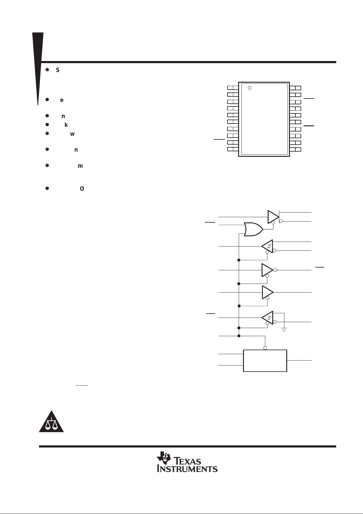
DY2
DZ2
RY1
DY1
RY2
DA2
DEN
RB1
RA1
DA1
RB2
SHDN
10
9
12
13
11
1
5
18
15
14
7
6
DY3
DA3
16 17
Charge Pump V
EE
V
CC
GND
2
8
19
logic diagram (positive logic)
1
2
3
4
5
6
7
8
9
10
20
19
18
17
16
15
14
13
12
11
DA1
V
EE
C–
C+
SHDN
DZ2
DY2
GND
DEN
DA2
GND
V
CC
DY1
DY3
DA3
RB2
RY2
RB1
RA1
RY1
DW PACKAGE
(TOP VIEW)
PRODUCTION DATA information is current as of publication date.
Products conform to specifications per the terms of Texas Instruments
standard warranty. Production processing does not necessarily include
testing of all parameters.
Copyright 1996, Texas Instruments Incorporated
GeoPort, LocalTalk, and AppleTalk are trademarks of Apple Computer , Incorporated.
LinBiCMOS is a trademark of Texas Instruments Incorporated.
Page 2
SN75LBC777
SINGLE CHIP GEOPORT/AppleTalk TRANSCEIVER
SLLS227 – SEPTEMBER 1996
2
POST OFFICE BOX 655303 • DALLAS, TEXAS 75265
description (continued)
A switched-capacitor voltage converter generates the negative voltage required from a single 5-V supply using
two 0.33-µF capacitors. One capacitor is between the C+ and C– terminals and the other is between V
EE
and
ground.
The SN75LBC777 is characterized for operation over the 0°C to 70°C temperature range.
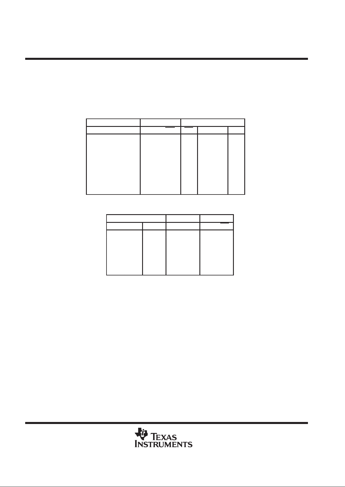
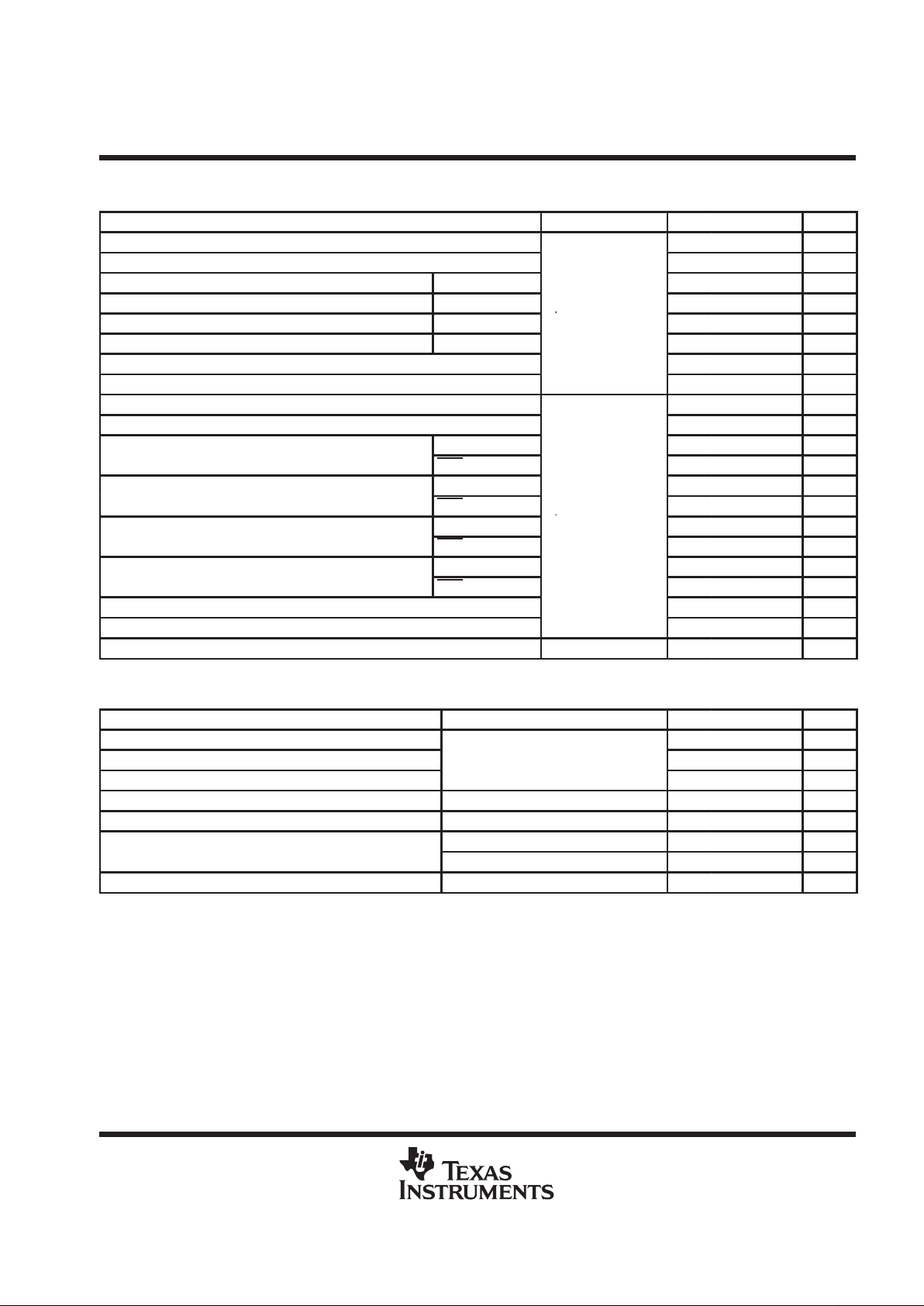
DRIVER FUNCTION TABLE
INPUTS
ENABLE OUTPUTS
DA1 DA2 DA3 SHDN DEN DY1 DY2 DZ2 DY3
H X H L X L X X H
L XL L XHXXL
X HX L LXHLX
X LX L LXLHX
OPEN OPEN OPEN L LLHLH
X XXH XZZZZ
X XXX HXZZX
X X XOPEN OPEN Z Z Z Z
H = high level, L= low level, X = irrelevant, ? = indeterminate, Z = high impedance (off)
RECEIVER FUNCTION TABLE
INPUTS
ENABLE OUTPUTS
RA1 RB1 RB2 SHDN RY1 RY2
H L H L H L
L HL L LH
OPEN OPEN L H H
SHORT
†
SHORT
†
L ? ?
X XX H ZZ
XXX OPEN Z Z
†
–0.2 V < VID < 0.2 V
H = high level, L= low level, X = irrelevant, ? = indeterminate,
Z = high impedance (off)
Page 3
SN75LBC777
SINGLE CHIP GEOPORT/AppleTalk TRANSCEIVER
SLLS227 – SEPTEMBER 1996
3
POST OFFICE BOX 655303 • DALLAS, TEXAS 75265
absolute maximum ratings over operating free-air temperature range (unless otherwise noted)
†
Positive supply voltage range, V
CC,
(see Note 1) –0.5 to 7 V. . . . . . . . . . . . . . . . . . . . . . . . . . . . . . . . . . . . . . . . .
Negative supply voltage range, V
EE,
(see Note 1) –7 to 0.5 V. . . . . . . . . . . . . . . . . . . . . . . . . . . . . . . . . . . . . . . .
Receiver input voltage range (RA1, RB1, RB2) –15 V to 15 V. . . . . . . . . . . . . . . . . . . . . . . . . . . . . . . . . . . . . . . .
Receiver differential input voltage range, V
ID
–12 V to 12 V. . . . . . . . . . . . . . . . . . . . . . . . . . . . . . . . . . . . . . . . . .
Receiver output voltage range (RY1, RY2
) –0.5 V to 5.5 V. . . . . . . . . . . . . . . . . . . . . . . . . . . . . . . . . . . . . . . . . . .
Driver output voltage range (Power Off)(DY1
, DY2, DZ2, DY3) –15 V to 15 V. . . . . . . . . . . . . . . . . . . . . . . . . . .
Driver output voltage range (Power On)(DY1
, DY2, DZ2, DY3) –11 V to 11 V. . . . . . . . . . . . . . . . . . . . . . . . . . .
Driver input voltage range (DA, SHDN, DEN
) –0.5 V to V
CC
+0.4 V. . . . . . . . . . . . . . . . . . . . . . . . . . . . . . . . . . .
Electrostatic discharge (see Note 2)
Bus Pins (Class 3 A) 10 kV. . . . . . . . . . . . . . . . . . . . . . . . . . . . . . . . . . . . . . . . . . . . . . . . .
Bus Pins (Class 3 B) 600 V. . . . . . . . . . . . . . . . . . . . . . . . . . . . . . . . . . . . . . . . . . . . . . . . .
All Pins (Class 3, A) 2 kV. . . . . . . . . . . . . . . . . . . . . . . . . . . . . . . . . . . . . . . . . . . . . . . . . .
All Pins (Class 3 B) 200 V. . . . . . . . . . . . . . . . . . . . . . . . . . . . . . . . . . . . . . . . . . . . . . . . . .
Continuous total power dissipation See Dissipation Rating Table. . . . . . . . . . . . . . . . . . . . . . . . . . . . . . . . . . . . .
Operating free-air temperature range, T
A
0°C to 70°C. . . . . . . . . . . . . . . . . . . . . . . . . . . . . . . . . . . . . . . . . . . . . .
Storage temperature range, T
stg
–65°C to 150 °C. . . . . . . . . . . . . . . . . . . . . . . . . . . . . . . . . . . . . . . . . . . . . . . . . .
Lead temperature 1,6 mm (1/16 inch) from case for 10 seconds 260°C. . . . . . . . . . . . . . . . . . . . . . . . . . . . . . .
†
Stresses beyond those listed under “absolute maximum ratings” may cause permanent damage to the device. These are stress ratings only, and
functional operation of the device at these or any other conditions beyond those indicated under “recommended operating conditions” is not
implied. Exposure to absolute-maximum-rated conditions for extended periods may affect device reliability.
NOTES: 1. All voltages values are with respect to the network ground terminal unless otherwise noted.
2. This rating is measured using MIL-STD-883C Method, 3015.7.
DISSIPATION RATING TABLE
PACKAGE
TA ≤ 25°C
POWER RATING
DERATE FACTOR
ABOVE TA = 25°C
TA = 70°C
POWER RATING
DW 1125 mW 9.0°C 720 mW
Page 4
SN75LBC777
SINGLE CHIP GEOPORT/AppleTalk TRANSCEIVER
SLLS227 – SEPTEMBER 1996
4
POST OFFICE BOX 655303 • DALLAS, TEXAS 75265
recommended operating conditions
MIN NOM MAX UNIT
Supply voltage, V
CC
4.75 5 5.25 V
High-level input voltage, VIH(DA, SHDN, DEN) 2 5.25 V
Low-level input voltage, V
IL
(DA, SHDN, DEN) 0.8 V
Receiver common-mode input voltage, V
IC
–7 7 V
Receiver differential input voltage, V
ID
–12 12 V
Voltage converter filter capacitance 0.33 µF
Voltage converter filter capacitor equivalent series resistance (ESR) 0 0.2 Ω
Operating free-air temperature, T
A
70 °C
driver electrical characteristics over operating free-air temperature range (unless otherwise
noted)
PARAMETER TEST CONDITIONS MIN TYP MAX UNIT
p
RL= 12 kΩ 3.6 4.5 V
VOHHigh-level output voltage
Single ended,
RL= 120 Ω 2 3.6 V
p
g,
See Figure 1
RL= 12 kΩ –4.5 –3.6 V
VOLLow-level output voltage
RL = 120 Ω –2.7 –1.8 V
|VOD|
Magnitude of differential output voltage
|VDY – VDZ|
R
= 120 Ω, See Figure 2
4 V
∆|VOD| Change in differential voltage magnitude
L
,
g
250 mV
V
OC
Common-mode output voltage –1 3 V
|∆V
OC(SS)
|
Magnitude of change, common-mode steadystate output voltage
See Figure 3
200 mV
|∆V
OC(PP)
|
Magnitude of change, common-mode
peak-to-peak output voltage
700 mV
pp
SHDN = DEN = 0 V, No Load 7 15 mA
ICCSupply current
SHDN = DEN = 5 V, No Load 100 µA
I
OZ
High-impedance output current VCC = 0 or 5 V, –10 ≤VO ≤ 10 V ±100 µA
I
OS
Short-circuit output current
VCC = 5.25 V ,
See Note 3
–5 V ≤VO ≤ 5 V,
±170 ±450 mA
NOTE 3: Not more than one output should be shorted at one time.
Page 5
SN75LBC777
SINGLE CHIP GEOPORT/AppleTalk TRANSCEIVER
SLLS227 – SEPTEMBER 1996
5
POST OFFICE BOX 655303 • DALLAS, TEXAS 75265
driver switching characteristics over recommended operating conditions (unless otherwise
noted)
PARAMETER TEST CONDITIONS MIN TYP MAX UNIT
t
PHL
Propagation delay time, high-to-low level output 40 75 ns
t
PLH
Propagation delay time, low-to-high level output 40 75 ns
t
PZL
Driver output enable time to low-level output SHDN 25 100 µs
t
PZH
Driver output enable time to high-level output SHDN
Single-ended,
25 100 µs
t
PLZ
Driver output disable time from low-level output SHDN
R
L
=
120 Ω
,
See
Figure 4
30 100 ns
t
PHZ
Driver output disable time from high-level output SHDN
See Figure 4
30 100 ns
t
r
Rise time 10 25 75 ns
t
f
Fall time 10 25 75 ns
t
PHL
Propagation delay time, high-to-low level output 40 75 ns
t
PLH
Propagation delay time, low-to-high level output 40 75 ns
p
p
SHDN 25 100 µs
t
PZL
Driver output enable time to low-level output
DEN 35 100 ns
p
p
SHDN 25 100 µs
t
PZH
Driver output enable time to high-level output
DEN
Differential,
35 150 ns
p
p
SHDN
R
L
=
120 Ω
,
See
Figure
5
30 100 ns
t
PLZ
Driver output disable time from low-level output
DEN
See Figure 5
30 100 ns
p
p
SHDN 35 100 ns
t
PHZ
Driver output disable time from high-level output
DEN 35 100 ns
t
r
Rise time 10 25 75 ns
t
f
Fall time 10 25 75 ns
t
SK(P)
Pulse skew, |t
PLH
– t
PHL
| 22 ns
receiver electrical characteristics over free-air temperature range (unless otherwise noted)
PARAMETER TEST CONDITIONS MIN TYP MAX UNIT
V
IT+
Positive-going input threshold voltage 200 mV
V
IT–
Negative-going input threshold voltage –200 mV
V
hys
Differential input voltage hysteresis (V
IT+
– V
IT–
) 50 mV
V
OH
High-level output voltage (see Note 4) IOH = 2 mA, VIC = 0 2 4.9 V
V
OL
Low-level output voltage IOL = –2 mA, VIC = 0 0.2 0.8 V
p
VO = 0 –85 –45 mA
IOSShort-circuit output current
VO = 5.25 V 45 85 mA
R
I
Input resistance VCC = 0 or 5.25 V, –12 V ≤ VI ≤ 12 V 6 30 kΩ
NOTE 4: If the inputs are left unconnected, RA1 interprets this as a high-level input and RB1 and RB2 interpret this as a low-level input so that
all outputs are at the high level.
Page 6

SN75LBC777
SINGLE CHIP GEOPORT/AppleTalk TRANSCEIVER
SLLS227 – SEPTEMBER 1996
6
POST OFFICE BOX 655303 • DALLAS, TEXAS 75265
receiver switching characteristics over free-air temperature range (unless otherwise noted)
PARAMETER TEST CONDITIONS MIN TYP MAX UNIT
t
PHL
Propagation delay time, high-to-low level output 30 75 ns
t
PLH
Propagation delay time, low-to-high level output
30 75 ns
t
r
Rise time
RL = 2 kΩ,
CL = 15 pF,
15 30 ns
t
f
Fall time
See Figure 6
15 30 ns
t
sk(p)
Pulse skew |t
PLH-tPHL
| 20 ns
t
PZL
Receiver output enable time to low-level output 35 100 ns
t
PZH
Receiver output enable time to high-level output
Differential, CL = 50 pF,
35 100 ns
t
PLZ
Receiver output disable time from low-level output
See Figure 7
L
21 100 ns
t
PHZ
Receiver output disable time from high-level output 21 100 ns
t
PZL
Receiver output enable time to low-level output 12 25 µs
t
PZH
Receiver output enable time to high-level output
Single-ended, C
= 50 pF,
12 25 µs
t
PLZ
Receiver output disable time from low-level output
g,
See Figure 7
L
,
25 100 ns
t
PHZ
Receiver output disable time from high-level output 125 400 ns
Page 7

SN75LBC777
SINGLE CHIP GEOPORT/AppleTalk TRANSCEIVER
SLLS227 – SEPTEMBER 1996
7
POST OFFICE BOX 655303 • DALLAS, TEXAS 75265
PARAMETER MEASUREMENT INFORMATION
V
I
I
I
I
O
DY1
V
O
C
L
R
L
DA1
SHDN
V
I
V
O
V
O
C
L
C
L
R
L
R
L
DY2
I
O
I
O
DZ2
I
I
SHDN
DA2
TEST CIRCUIT
DEN
or
NOTES: A. CL = 50 pF
B. Driver 3 is a noninverting version of driver 1.
Figure 1. Single-Ended Driver DC Parameter Test Circuits
V
I
V
OD
DY2
DZ2
I
I
DA2
60 Ω
60 Ω
50 pF
TEST CIRCUIT
I
O
SHDN
DEN
or
Figure 2. Differential Driver DC Parameter Test Circuit
V
I
V
OD
DY2
DZ2
DA2
60 Ω
60 Ω
15 pF
TEST CIRCUIT (see Note A)
V
OC
1.5 V
1.5 V
V
OC(PP)
V
OC(SS)
3 V
0 V
0 V
V
I
V
OC
VOLTAGE WAVEFORM
SHDN
DEN
or
NOTE A. Measured 3dB Bandwidth = 300 MHz
Figure 3. Differential Driver Common-Mode Output Voltage Test Circuit and Waveform
Page 8

SN75LBC777
SINGLE CHIP GEOPORT/AppleTalk TRANSCEIVER
SLLS227 – SEPTEMBER 1996
8
POST OFFICE BOX 655303 • DALLAS, TEXAS 75265
PARAMETER MEASUREMENT INFORMATION
t
PHL
DY1
V
O
C
L
R
L
DA1
SHDN
V
I
V
O
V
O
C
L
C
L
R
L
R
L
DY2
I
O
I
O
DZ2
I
I
DA2
TEST CIRCUIT
(see Note A)
t
PHL
t
PLZ
t
PZL
t
PLH
t
PHZ
1.5 V 1.5 V 1.5 V 1.5 V
1.5 V 1.5 V
3 V
0 V
3 V
0 V
DA
DY2
V
OH
V
OL
0 V
t
PZL
t
r
t
f
90% 90%
10%
90%
90%
10% 10% 10%
V
OH
V
OL
0 V
VOLTAGE WAVEFORM
(see Note B)
50%
50%
DY1
, DZ2
SHDN
or
DEN
SHDN
or
DEN
90%
10%
50%
90%
10%
50%
90%
90%
10%
t
PZH
t
PLH
t
f
t
PHZ
10%
t
PZH
t
r
t
PLZ
NOTES: A. CL = 50 pF, RL = 120 Ω
B. The input waveform tr, tf ≤ 10 ns.
C. Driver 3 is a noninverting version of driver 1.
Figure 4. Single-Ended Driver Propagation and Transition Times Test Circuits and Waveform
Page 9

SN75LBC777
SINGLE CHIP GEOPORT/AppleTalk TRANSCEIVER
SLLS227 – SEPTEMBER 1996
9
POST OFFICE BOX 655303 • DALLAS, TEXAS 75265
PARAMETER MEASUREMENT INFORMATION
TEST CIRCUIT
t
PLH
t
PHZ
t
PZH
t
PHL
t
PLZ
t
PZL
t
r
t
f
1.5 V 1.5 V 1.5 V 1.5 V
1.5 V 1.5 V
90% 90%
10%
90%
90%
10% 10% 10%
3 V
0 V
3 V
0 V
V
OD(H)
V
OD(L)
0 V
DA
VOLTAGE WAVEFORM
V
I
V
OD
DY2
DZ2
DA2
RL = 60 Ω
50 pF
RL = 60 Ω
50%
50%
SHDN
or
DEN
SHDN
or
DEN
V
OD
NOTE A: For the input waveform tr, tf < = 10 ns
Figure 5. Differential Driver Propagation and Transition Times Test Circuit and Waveforms
_
+
V
I
I
I
I
O
V
O
V
CC
2 kΩ
15 pF
RY
RA
RB
Input
SHDN
Output
t
r
t
f
t
PLH
t
PHL
0 V 0 V
2.5 V
–2.5 V
V
OH
1.5 V
V
OL
90% 90%
10% 10%
V
I
V
O
TEST CIRCUIT VOLTAGE WAVEFORM
NOTE A: For the input waveform tr, tf < = 10 ns
Figure 6. Receiver Propagation and Transition Times Test Circuit and Waveform
Page 10

SN75LBC777
SINGLE CHIP GEOPORT/AppleTalk TRANSCEIVER
SLLS227 – SEPTEMBER 1996
10
POST OFFICE BOX 655303 • DALLAS, TEXAS 75265
PARAMETER MEASUREMENT INFORMATION
_
+
CL = 50 pF
RY
RA
RB
–2.5 V or 2.5 V
SHDN
t
PLZ
t
PZL
1.5 V
3 V
0 V
V
CC
V
OL
10%
90%
SHDN
V
O
TEST CIRCUIT
VOLTAGE WAVEFORM
RL = 500 Ω
V
CC
10%
90%
1.5 V
t
PHZ
t
PZH
S1 at V
CC
S1 at GND
V
OH
0 V
S1
NOTE A: For the input waveform tr, tf < = 10 ns
Figure 7. Receiver Enable and Disable Test Circuit and Waveforms
Page 11

SN75LBC777
SINGLE CHIP GEOPORT/AppleTalk TRANSCEIVER
SLLS227 – SEPTEMBER 1996
11
POST OFFICE BOX 655303 • DALLAS, TEXAS 75265
APPLICATION INFORMATION
GeoPort
Host
SN75LBC776
9-Terminal
DTE
678
34 9 5
12
13
12
7
6
18
15
16
RxD
RxD+
TxD+
TxD
GND
RESET/ATT
SCLK
Power
TxHS/Wake-Up
6
13
15
18
19
17
RxD–
TxD–
SHDN
DTR
RTXC
CTS
RTS
Standard
Peripheral
SN75LBC777
9-Terminal
DCE
6
7
12
13
15
18
17 TxHS/WAKE-UP
Power
V
CC
GND
RxD–
RxD+
TxD+
TxD–
RESET/ATT
SCLK
V
CC
V
EE
19
4
3
2
8
20
0.33 µF
+
+
0.33 µF
RESET/ATT
SCLK
TxHS/WAKE-UP
–5 V
10
11
5
14
1
9
7
12
16
GeoPort
Peripheral
Device
SN75LBC777
9-Terminal
DCE
GeoPort
Control
Logic
DEN
NOTE A: A potential charge pump capacitor is the AVX 0805YC334MATXA or an equivalent.
Figure 8. GeoPort 9-terminal DCE Connection Application
Page 12

SN75LBC777
SINGLE CHIP GEOPORT/AppleTalk TRANSCEIVER
SLLS227 – SEPTEMBER 1996
12
POST OFFICE BOX 655303 • DALLAS, TEXAS 75265
generator characteristics
232/V.28 423/V.10 562
PARAMETER
TEST CONDITIONS
MIN MAX MIN MAX MIN MAX
UNIT
Open circuit 25 4 6 13.2 V
|VO| Output voltage magnitude
3 kΩ ≤ RL ≤ 7 kΩ
5 15 NA 3.7 V
RL = 450 Ω NA 3.6 NA V
I
OS
Short-circuit output current VO = 0 100 150 60 mA
R
O(OFF)
Power-off source resistance VCC = 0, |VO| < 2 V 300 NA 300 Ω
I
O(OFF)
Power-off output current VCC = 0, |VO| < 6 V NA ±100 NA µA
SR Output voltage slew rate 30 NA 4 30 V/µs
±3.3 V to ±3.3 V NA NA 0.22 2.1 µs
t
t
Output transition time
±3 V to ±3 V
0.04 NA NA ui
†
10% to 90% NA 0.3 NA ui
†
V
O(RING)
Output voltage ringing NA 10% 5%
†
ui is the unit interval and is the inverse of the signaling rate (a.k.a. bit time).
receiver characteristics
232/V.28 423/V.10 562
PARAMETER
TEST CONDITIONS
MIN MAX MIN MAX MIN MAX
UNIT
|VI| Input voltage 25 10 25 V
p
|VI| < 15 V –3 3 NA –3 3 V
VITInput voltage threshold
|VI| < 10 V NA –0.2 0.2 NA V
p
3 V < |VI| < 15 V 3 7 NA 3 7 kΩ
RIInput resistance
|VI| < 10 V NA 4 NA kΩ
Page 13

SN75LBC777
SINGLE CHIP GEOPORT/AppleTalk TRANSCEIVER
SLLS227 – SEPTEMBER 1996
13
POST OFFICE BOX 655303 • DALLAS, TEXAS 75265
MECHANICAL INFORMATION
DW (R-PDSO-G**) PLASTIC SMALL-OUTLINE PACKAGE
16 PIN SHOWN
4040000/B 03/95
Seating Plane
0.400 (10,15)
0.419 (10,65)
0.104 (2,65) MAX
1
0.012 (0,30)
0.004 (0,10)
A
8
16
0.020 (0,51)
0.014 (0,35)
0.293 (7,45)
0.299 (7,59)
9
0.010 (0,25)
0.050 (1,27)
0.016 (0,40)
(15,24)
(15,49)
PINS **
0.010 (0,25) NOM
A MAX
DIM
A MIN
Gage Plane
20
0.500
(12,70)
(12,95)
0.510
(10,16)
(10,41)
0.400
0.410
16
0.600
24
0.610
(17,78)
28
0.700
(18,03)
0.710
0.004 (0,10)
M
0.010 (0,25)
0.050 (1,27)
0°–8°
NOTES: A. All linear dimensions are in inches (millimeters).
B. This drawing is subject to change without notice.
C. Body dimensions do not include mold flash or protrusion not to exceed 0.006 (0,15).
D. Falls within JEDEC MS-013
Page 14

IMPORTANT NOTICE
T exas Instruments (TI) reserves the right to make changes to its products or to discontinue any semiconductor
product or service without notice, and advises its customers to obtain the latest version of relevant information
to verify, before placing orders, that the information being relied on is current and complete.
TI warrants performance of its semiconductor products and related software to the specifications applicable at
the time of sale in accordance with TI’s standard warranty. Testing and other quality control techniques are
utilized to the extent TI deems necessary to support this warranty. Specific testing of all parameters of each
device is not necessarily performed, except those mandated by government requirements.
Certain applications using semiconductor products may involve potential risks of death, personal injury, or
severe property or environmental damage (“Critical Applications”).
TI SEMICONDUCTOR PRODUCTS ARE NOT DESIGNED, INTENDED, AUTHORIZED, OR WARRANTED
TO BE SUITABLE FOR USE IN LIFE-SUPPORT APPLICATIONS, DEVICES OR SYSTEMS OR OTHER
CRITICAL APPLICATIONS.
Inclusion of TI products in such applications is understood to be fully at the risk of the customer. Use of TI
products in such applications requires the written approval of an appropriate TI officer. Questions concerning
potential risk applications should be directed to TI through a local SC sales office.
In order to minimize risks associated with the customer’s applications, adequate design and operating
safeguards should be provided by the customer to minimize inherent or procedural hazards.
TI assumes no liability for applications assistance, customer product design, software performance, or
infringement of patents or services described herein. Nor does TI warrant or represent that any license, either
express or implied, is granted under any patent right, copyright, mask work right, or other intellectual property
right of TI covering or relating to any combination, machine, or process in which such semiconductor products
or services might be or are used.
Copyright 1998, Texas Instruments Incorporated
 Loading...