

Page 1
SN75DP129
www.ti.com
SLAS583A – JANUARY 2008 – REVISED MARCH 2008
DisplayPort to TMDS Translator
1
FEATURES APPLICATIONS
• DisplayPort Physical Layer Input Port to TMDS
Physical Layer Output Port
• Integrated TMDS Level Translator With
Receiver Equalization
• Supports Data Rates up to 2.5 Gbps
• Integrated I2C Logic Block for DVI / HDMI
Connector Recognition
• Integrated Active I2C Buffer
• Enhanced ESD: 12 kV on all Pins
• Enhanced Commercial Temperature Range:
0 ° C to 85 ° C
• 36 Pin 6 × 6 QFN Package
DESCRIPTION
The SN75DP129 is a Dual-Mode DisplayPort input to Transition-Minimized Differential Signaling (TMDS) output.
The TMDS output has a built-in level translator, compliant with Digital Visual Interface 1.0 (DVI) and High
Definition Multimedia Interface 1.3 (HDMI) standards. The SN75DP129 is specified up to a maximum data rate of
2.5 Gbps, supporting resolutions greater then 1920 x 1200 or HDTV 12-bit color depth at 1080p (progressive
scan).
An integrated Active I2C buffer isolates the capacitive loading of the source system from that of the sink and
interconnecting cable. This isolation improves overall signal integrity of the system and provides greater design
margin within the source system for DVI / HDMI compliance testing.
A logic block was designed into the SN75DP129 to assist with TMDS connector identification. Through the use of
the I2C_EN pin, this logic block can be enabled to indicate the translated port is an HDMI port; therefore legally
supporting HDMI content.
• Personal Computer Market
– DP/TMDS Hardware Key (Dongle)
– Desktop PC
– Notebook PC
– Docking Station
– Standalone Video Card
1
Please be aware that an important notice concerning availability, standard warranty, and use in critical applications of Texas Instruments semiconductor products and disclaimers thereto appears at the end of this data sheet.
PRODUCTION DATA information is current as of publication date.
Products conform to specifications per the terms of the Texas
Instruments standard warranty. Production processing does not
necessarily include testing of all parameters.
Copyright © 2008, Texas Instruments Incorporated
Page 2
www.ti.com
Dongle
Computer Notebook
DockingStation
GPU
SN75DP129
TMDSBuffer
DVIorHDMI
Compliant
MonitororHDTV
DP++
TMDS
SN75DP129
SLAS583A – JANUARY 2008 – REVISED MARCH 2008
These devices have limited built-in ESD protection. The leads should be shorted together or the device placed in conductive foam
during storage or handling to prevent electrostatic damage to the MOS gates.
TYPICAL APPLICATION
GPU — Graphics Processing Unit
DP++ — Dual-Mode DisplayPort
TMDS — Transition-Minimized Differential Signaling
DVI — Digital Visual Interface
HDMI — High Definition Multimedia Interface
2 Submit Documentation Feedback Copyright © 2008, Texas Instruments Incorporated
Product Folder Link(s): SN75DP129
Page 3

www.ti.com
INTERNAL DATA CONNECTION DIAGRAM
GND
LP
TMDS_2(n)
VSadj
SDA
SCL
HPD_IN
VDD
HPD_OUT
GND
VCC
ML_IN0(p)
I2C_EN
VCC
I2C
Slave
TMDS_2(p)
ML_IN0(n)
ML_IN1(p)
ML_IN1(n)
VCC
ML_IN2(p)
ML_IN2(n)
GND
ML_IN3(p)
ML_IN3(n)
VCC
GND
TMDS_CLK(n)
TMDS_CLK(p)
VCC
TMDS_0(n)
TMDS_0(p)
GND
TMDS_1(n)
TMDS_1(p)
SN75DP129
AUX_I C(p)
2
1
AUX_I C(n)
2
1
SN75DP129
SLAS583A – JANUARY 2008 – REVISED MARCH 2008
(1) I2C bus data (n-SDA) and clock (p-SCL) lines.
Copyright © 2008, Texas Instruments Incorporated Submit Documentation Feedback 3
Product Folder Link(s): SN75DP129
Page 4
www.ti.com
1
I2C_EN
VDD
ML_IN0(p)
HPD_OUT
SDA
VSadj
VCC
TMDS_2(n)
SCL
2 3 4 5 6 7 8
11
10
12
13
14
15
16
17
35
36
34
33
32
31
30
29
2627 24 23 22 21 2025
9
18
19
28
GND
VCC
LP
TMDS_2(p)
ML_IN0(n)
ML_IN1(p)
ML_IN1(n)
VCC
ML_IN2(p)
ML_IN2(n)
GND
ML_IN3(p)
ML_IN3(n)
VCC
GND
HPD_IN
GND
TMDS_CLK(n)
TMDS_CLK(p)
VCC
TMDS_0(n)
TMDS_0(p)
GND
TMDS_1(n)
TMDS_1(p)
SN75DP129
RHHPACKAGE
(TopView)
AUX_I2C(p)
1
AUX_I2C(n)
1
SN75DP129
SLAS583A – JANUARY 2008 – REVISED MARCH 2008
PIN CONFIGURATION
(1) I2C bus data (n-SDA) and clock (p-SCL) lines.
TERMINAL FUNCTIONS
TERMINAL
NAME NO.
2C(2)
AUX_I
GND 6, 10, 19, 25, 36 Ground Ground
HPD_IN 15 I Hot Plug Detect (HPD) Input Hot Plug Detect
HPD_OUT 13 O Hot Plug Detect (HPD) Output Hot Plug Detect
I2C_EN 32 I Control
LP 33 I Low Power Select Bar Control
ML_IN 0 34(p), 35(n) I DisplayPort Main Link Channel 0 Differential Input Main Link Input Pins
ML_IN 1 1(p), 2(n) I DisplayPort Main Link Channel 1 Differential Input Main Link Input Pins
ML_IN 2 4(p), 5(n) I DisplayPort Main Link Channel 2 Differential Input Main Link Input Pins
ML_IN 3 7(p), 8(n) I DisplayPort Main Link Channel 3 Differential Input Main Link Input Pins
TMDS_2 30(p), 29(n) O TMDS Data 2 Differential Output Main Link Output
TMDS_1 27(p), 26(n) O TMDS Data 1 Differential Output Main Link Output
TMDS_0 24(p), 23(n) O TMDS Data 0 Differential Output Main Link Output
TMDS_CLK 21(p), 20(n) O TMDS Data Clock Differential Output Main Link Output
SCL 17 I/O TMDS Port Bidirectional I2C Clock Line DDC Link (Sink)
SDA 16 I/O TMDS Port Bidirectional I2C Data Line DDC Link (Sink)
VCC 3, 9, 18, 22, 28 3.3 V Supply Voltage Supply
(1) (p) Positive; (n) Negative
(2) I2C bus data (n-SDA) and clock (p-SCL) lines.
(1)
11(p), 12(n) I/O Source Side Bidirectional DisplayPort Auxiliary Data Line DDC LINK (Source)
I/O DESCRIPTION TYPE
Internal I2C register enable, used for HDMI / DVI connector
differentiation
4 Submit Documentation Feedback Copyright © 2008, Texas Instruments Incorporated
Product Folder Link(s): SN75DP129
Page 5
www.ti.com
+
–
V
CC
50 W 50 W
V
TERM
V
TERM
Z
Y
10mA
SLAS583A – JANUARY 2008 – REVISED MARCH 2008
TERMINAL FUNCTIONS (continued)
TERMINAL
NAME NO.
VDD 14 HPD Supply Voltage Supply
VSadj 31 I TMDS-Compliant Voltage Swing Control Reference
(1)
I/O DESCRIPTION TYPE
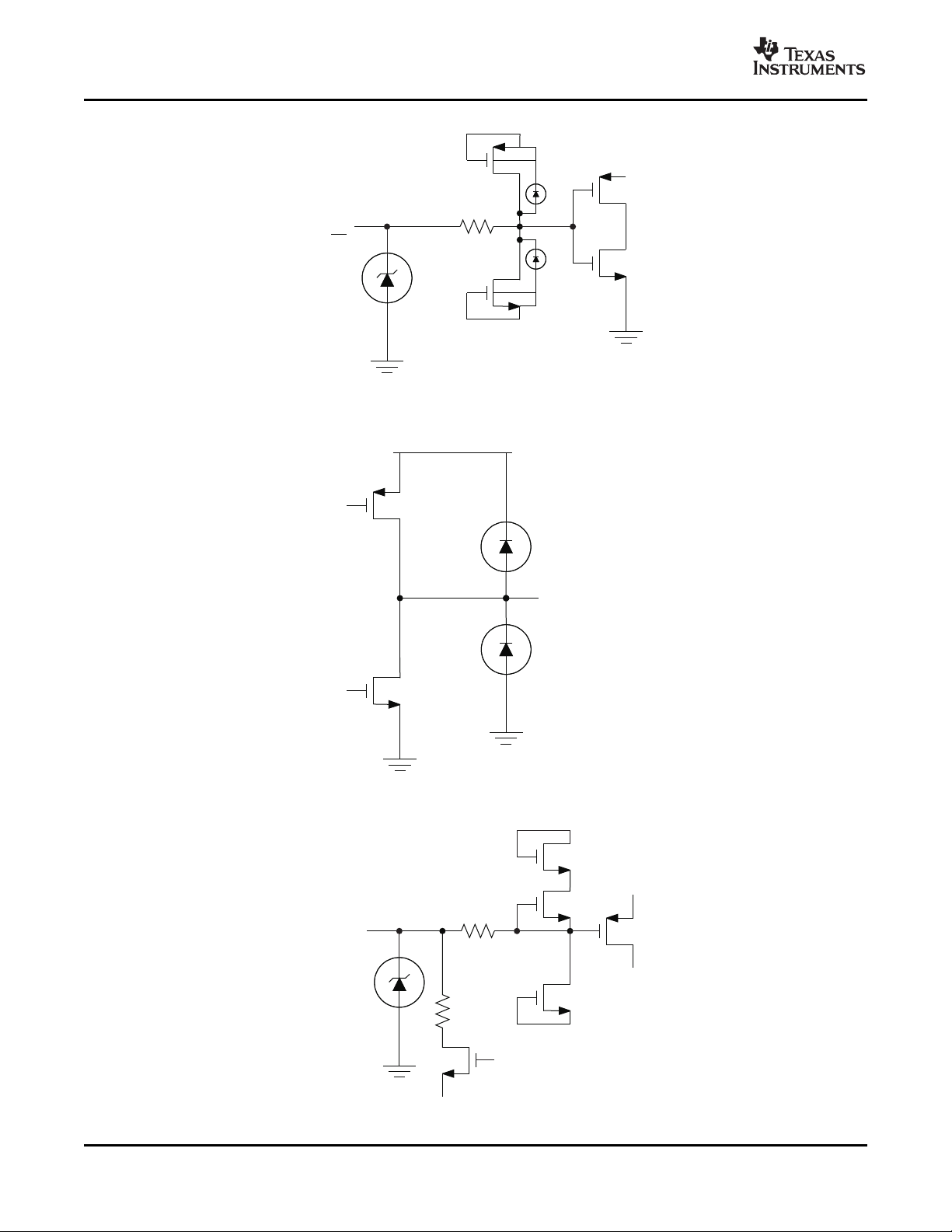
Input/Output Equivalent Circuits
SN75DP129
Figure 1. DisplayPort Input Stage
Figure 2. TMDS Output Stage
Copyright © 2008, Texas Instruments Incorporated Submit Documentation Feedback 5
Product Folder Link(s): SN75DP129
Page 6
www.ti.com
I C_EN
2
LP
HPD_OUT
V
DD
SCL
SDA
AUX+/–
400 W
V
OL
SN75DP129
SLAS583A – JANUARY 2008 – REVISED MARCH 2008
Figure 3. HPD and Control Input Stage
Figure 4. HPD Output Stage
Figure 5. I2C Input and Output Stage
6 Submit Documentation Feedback Copyright © 2008, Texas Instruments Incorporated
Product Folder Link(s): SN75DP129
Page 7
www.ti.com
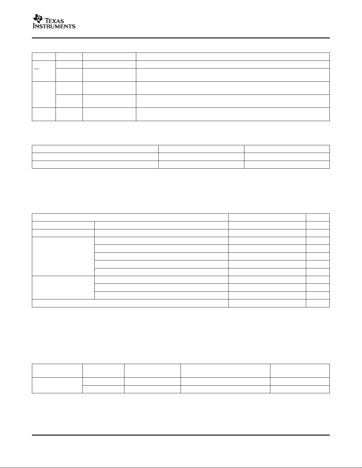
Table 1. Control Pin Lookup Table
SIGNAL LEVEL STATE DESCRIPTION
H Normal Mode Normal operational mode for device
LP
L Low Power Mode
H HDMI
I2C_EN
L DVI
VS
adj
4.65 k Ω Driver output voltage swing precision control to aid with system compliance.
(1) (H) Logic High; (L) Logic Low
Compliant Voltage
Swing
Device is forced into a Low Power state causing the outputs to go to a high impedance
state. All other inputs are ignored.
Internal I2C register is active and readable, indicating the connector in use is
HDMI-compliant.
Internal I2C register is disabled and unreadable, indicating the connector in use is
DVI-compliant.
SN75DP129
SLAS583A – JANUARY 2008 – REVISED MARCH 2008
(1)
ORDERING INFORMATION
(1)
PART NUMBER PART MARKING PACKAGE
SN75DP129RHHR DP129 36-pin QFN Reel (large)
SN75DP129RHHT DP129 36-pin QFN Reel (small)
(1) For the most current package and ordering information, see the Package Option Addendum at the end of this document, or see the TI
web site at www.ti.com .
ABSOLUTE MAXIMUM RATINGS
over operating free-air temperature range (unless otherwise noted)
Supply voltage range
Supply voltage range VDD – 0.3 to 3.6 V
Voltage range HPD I/O – 0.3 to 5.5 V
Electrostatic discharge Charged-device model
Continuous power dissipation See Dissipation Ratings Table
(1) Stresses beyond those listed under absolute maximum ratings may cause permanent damage to the device. These are stress ratings
only and functional operation of the device at these or any conditions beyond those indicated under recommended operating conditions
is not implied. Exposure to absolute-maximum-rated conditions for extended periods may affect device reliability.
(2) All voltage values, except differential voltages, are with respect to network ground terminal.
(3) Tested in accordance with JEDEC Standard 22, Test Method A114-B
(4) Tested in accordance with JEDEC Standard 22, Test Method C101-A
(5) Tested in accordance with JEDEC Standard 22, Test Method A115-A
(2)
VCC – 0.3 to 3.6 V
Main link I/O (ML_IN x, DP_SINK x) differential voltage 1.5 V
TMDS I/O – 0.3 to 4 V
Auxiliary I/O – 0.3 to 5.5 V
Control I/O – 0.3 to 5.5 V
Human body model
Machine model
(3)
(4)
(5)
(1)
VALUE UNIT
± 12000 V
± 1000 V
± 200 V
DISSIPATION RATINGS
PACKAGE TA≤ 25 ° C
36-pin QFN (RHH)
PCB JEDEC
STANDARD
Low-K 1398 mW 13.98 mW/ ° C 559 mW
High-K 2941 mW 29.41 mW/ ° C 1176 mW
DERATING FACTOR
ABOVE TA= 25 ° C POWER RATING
(1) This is the inverse of the junction-to-ambient thermal resistance when board-mounted and with no air flow.
Copyright © 2008, Texas Instruments Incorporated Submit Documentation Feedback 7
Product Folder Link(s): SN75DP129
(1)
TA= 85 ° C
Page 8
www.ti.com
SN75DP129
SLAS583A – JANUARY 2008 – REVISED MARCH 2008
THERMAL CHARACTERISTICS
over operating free-air temperature range (unless otherwise noted)
PARAMETER TEST CONDITIONS MIN TYP MAX UNIT
R
Junction-to-board thermal resistance 9.44
θ JB
R
Junction-to-case thermal resistance 24.74 ° C/W
θ JC
P
Device power dissipation
D
P
Device power dissipation under low power LP = 0 V 5 20 µ W
SD
(2)
(1) The maximum rating is simulated under 3.6 V V
(2) Power disipation is the sum of the power consumption from the V
Termination Supply).
RECOMMENDED OPERATING CONDITIONS
V
CC
V
DD
T
A
MAIN LINK DIFFERENTIAL INPUT PINS
V
ID
d
R
TMDS DIFFERENTIAL OUTPUT PINS
AV
d
R
R
t
AUXILIARY AND I2C PINS
V
I
d
R(I2C)
HPD AND CONTROL PINS
V
IH
V
IL
Supply voltage 3 3.3 3.6 V
Supply voltage 1.65 3.6 V
Operating free-air temperature 0 85 ° C
Peak-to-peak input differential voltage 0.15 1.40 V
Data rate 2.5 Gbps
TMDS output termination voltage 3 3.3 3.6 V
CC
Data rate 2.5 Gbps
Termination resistance 45 50 55 Ω
Input voltage 0 5.5 V
I2C data rate 100 kHz
High-level input voltage 2 5.5 V
Low-level input voltage 0 0.8 V
LP = 3.3 V, ML: VID= 500 mV, 2.5 Gbps
PRBS; 380 490 mW
I2C: VID= 3.3 V, 100 Kbps PRBS; HPD = 5 V
and V
CC
unless otherwise noted.
DD
(1)
and V
CC
pins, plus the 132 mW of power from the AVCC (Receiver
DD
° C/W
MIN NOM MAX UNIT
Device Power
The SN75DP129 is designed to operate from one or two supply voltages, depending on the implementation of
the integrated Hot Plug Detect (HPD) level translator. The TMDS level translator is powered from a single 3.3-V
supply. The HPD translator is powered using the VDD pin and its voltage can range from 1.8 V to 3.3 V. This
voltage determines the HIGH-level output voltage of the HPD_OUT pin.
ELECTRICAL CHARACTERISTICS
over recommended operating conditions (unless otherwise noted)
PARAMETER TEST CONDITIONS MIN TYP MAX UNIT
I
I
ISD Shutdown current LP = 0 V 1 5 µ A
8 Submit Documentation Feedback Copyright © 2008, Texas Instruments Incorporated
Supply current LP = 3.6 V, V
CC
= VDD, 50 75 112 mA
CC
ML: VID= 500 mV, 2.7 Gbps PRBS
Supply current 1 2 mA
DD
AUX: VI= 3.3 V, 100 kHz PRBS
HPD: HPD_IN = 5 V
Product Folder Link(s): SN75DP129
Page 9

www.ti.com
DP129
100kW
HPDInput
HPDOutput
100kW
t
PD(HPD)
50%
50%
5V
0V
V
DD
0V
HPD_IN
HPD_OUT
SN75DP129
SLAS583A – JANUARY 2008 – REVISED MARCH 2008
Hot Plug and Cable Adapter Detect
The SN75DP129 has a built-in level shifter for the HPD outputs. The output voltage level of the HPD pin is
defined by the voltage level of the VDD pin.
ELECTRICAL CHARACTERISTICS
over recommended operating conditions (unless otherwise noted)
PARAMETER TEST CONDITIONS MIN TYP MAX UNIT
V
OH3.3
V
OH2.5
V
OH1.8
V
OL
I
H
I
L
High-level output voltage IOH= – 100 A, V
Low-level output voltage IOH= 100 µ A 0 0.4 V
High-level input current VIH= 2.0 V, V
Low-level input current VIL= 0.8 V, V
SWITCHING CHARACTERISTICS
over recommended operating conditions (unless otherwise noted)
PARAMETER TEST CONDITIONS MIN TYP MAX UNIT
t
PD(HPD)
Propagation delay V
IOH= – 100 µ A, V
IOH= – 100 A, V
= 3.6 V 5 30 ns
DD
= 3.3 V 3 3.3 V
DD × 1
= 2.5 V 2.25 2.5 V
DD × 1
= 1.8 V 1.62 1.8 V
DD × 1
= 3.6 V – 10 10 µ A
DD
= 3.6 V – 10 10 µ A
DD
Figure 6. HPD Test Circuit
Figure 7. HPD Timing Diagram
AUX / I2C Pins
The SN75DP129 utilizes an active I2C repeater. The repeater isolates the parasitic effects of the system to aid
with system level compliance.
In addition to the I2C repeater, the SN75DP129 supports the connector detection I2C register. This register is
Product Folder Link(s): SN75DP129
enabled using the I2C_EN pin. When active, an internal memory register is readable using the AUX_I
This I2C register block functionality is described in the APPLICATION INFORMATION section.
Copyright © 2008, Texas Instruments Incorporated Submit Documentation Feedback 9
2
C pins.
Page 10

www.ti.com
PULSE
GENERATOR
D.U.T.
R
T
V
OUT
V
CC
3.3V
R =2kLW
C =100pF
L
V
IN
SN75DP129
SLAS583A – JANUARY 2008 – REVISED MARCH 2008
ELECTRICAL CHARACTERISTICS
over recommended operating conditions (unless otherwise noted)
PARAMETER TEST CONDITIONS MIN TYP MAX UNIT
I
L
I
lkg(AUX)
C
IO(AUX)
V
IH(AUX)
V
IL(AUX)
V
OL(AUX)
I
lkg(I2C)
C
IO(I2C)
V
IH(I2C)
V
IL(I2C)
V
OL(I2C)
SWITCHING CHARACTERISTICS
over recommended operating conditions (unless otherwise noted)
t
PLH1
t
PHL1
t
PLH2
t
PHL2
t
f1
t
f2
f
SCL
t
W(L)
t
W(H)
t
SU1
t
h(1)
t
(buf)
t
su(2)
t
h(2)
t
su(3)
Low input current V
Input leakage current AUX_I
Input/output capacitance AUX_I
High-level input voltage AUX_I
Low-level input voltage AUX_I
Low-level output voltage AUX_I
2
C pins V
2
C pins DC bias = 1.65 V, AC = 2.1 V
2
C pins 1.6 5.5 V
2
C pins – 0.2 0.4 V
2
C pins IO= 4 mA 0.5 0.6 V
Input leakage current I2C SDA/SCL pins V
Input/output capacitance I2C SDA/SCL pins DC bias = 2.5 V, AC = 3.5 V
High-level input voltage I2C SDA/SCL pins 2.1 5.5 V
Low-level input voltage I2C SDA/SCL pins – 0.2 1.5 V
Low-level output voltage I2C SDA/SCL pins IO= 4 mA 0.2 V
PARAMETER TEST CONDITIONS MIN TYP MAX UNIT
Propagation delay time, low to high Source to Sink 204 459 ns
Propagation delay time, high to low Source to Sink 35 200 ns
Propagation delay time, low to high Sink to Source 80 251 ns
Propagation delay time, high to low Sink to Source 35 200 ns
Output signal fall time Sink Side 20 72 ns
Output signal fall time Source Side 20 72 ns
SCL clock frequency for internal register Source Side 100 kHz
Clock LOW period for I2C register Source Side 4.7 µ s
Clock HIGH period for internal register Source Side 4.0 µ s
Internal register setup time, SDA to SCL Source Side 250 ns
Internal register hold time, SCL to SDA Source Side 0 µ s
Internal register bus free time between STOP and START Source Side 4.7 µ s
Internal register setup time, SCL to START Source Side 4.7 µ s
Internal register hold time, START to SCL Source Side 4.0 µ s
Internal register hold time, SCL to STOP Source Side 4.0 µ s
= 3.6 V, VI= 0 V – 10 10 µ A
CC
= 3.6 V, VI= 3.6 V – 10 10 µ A
CC
, f = 100 kHz 15 pF
p-p
= 3.6 V, VI= 4.95 V – 10 10 µ A
CC
, f = 100 kHz 15 pF
p-p
10 Submit Documentation Feedback Copyright © 2008, Texas Instruments Incorporated
Figure 8. Source Side Test Circuit (AUX_I
2
C)
Product Folder Link(s): SN75DP129
Page 11

www.ti.com
PULSE
GENERATOR
D.U.T.
R
T
V
OUT
V
CC
5V
R =2kLW
C =400pF
L
V
IN
Input
20%
80%
AUX_I2C (p)
Output
I2C_SCL
I2C_SDA
AUX_I2C(n)
t
f2
t
PHL2
t
PLH2
5V
1.6V
0.1V
3.3V
1.6V
V
OL
Input
20%
80%
AUX_I2C (p)
Output
AUX_I2C(n)
t
f1
t
PHL1
3.3V
1.6V
0.1V
5V
1.6V
V
OL
I2C_SCL
I2C_SDA
Input
AUX_I2C (p)
Output
AUX_I2C(n)
t
PLH1
3.3V
0.5V
1.6V
I2C_SCL
I2C_SDA
5V
Figure 9. Sink Side Test Circuit (SCL, SDA)
SN75DP129
SLAS583A – JANUARY 2008 – REVISED MARCH 2008
Figure 10. Source Side Output AC Measurements
Figure 11. Sink Side Output AC Measurements
Figure 12. Sink Side Output AC Measurements (continued)
Copyright © 2008, Texas Instruments Incorporated Submit Documentation Feedback 11
Product Folder Link(s): SN75DP129
Page 12

www.ti.com
SN75DP129
SLAS583A – JANUARY 2008 – REVISED MARCH 2008
TMDS and Main Link Pins
The main link inputs are designed to be compliant with the DisplayPort 1.1 specification. The TMDS outputs of
the SN75DP129 are designed to be compliant with the Digital Visual Interface 1.0 (DVI) and High Definition
Multimedia Interface 1.3 (HDMI) specifications. The differential output voltage swing can be fine-tuned with the
VSadj (TMDS-compliant Voltage Swing Control) resistor.
ELECTRICAL CHARACTERISTICS
over recommended operating conditions (unless otherwise noted)
PARAMETER TEST CONDITIONS MIN TYP MAX UNIT
V
OH
V
OL
V
SWING
V
OC(SS)
V
OD(PP)
V
(O)SBY
I
(O)OFF
I
OS
R
INT
V
term
Single-ended HIGH level output voltage AVCC – 10 AVCC+10 mV
Single-ended LOW level output voltage AVCC – 600 AVCC – 400 mV
Single-ended output voltage swing 400 600 mV
Change in steady-state common-mode
output voltage between logic states
AVCC = 3.3 V, RT= 50 Ω
– 5 5 mV
Peak-to-peak output differential voltage 800 1200 mV
Single-ended standby output voltage AVCC – 10 AVCC+10 mV
Single-ended power down output current – 10 10 µ A
AVCC = 3.3 V, RT= 50 Ω ,
LP = 0
0 V ≤ V
≥ 1.5 V, AVCC = 3.3 V,
CC
RT= 50 Ω
Short circuit output current VID= 500 mV – 15 15 mA
Input termination impedance 45 50 55 Ω
Input termination voltage 1 2 V
SWITCHING CHARACTERISTICS
over recommended operating conditions (unless otherwise noted)
PARAMETER TEST CONDITIONS MIN TYP MAX UNIT
t
PLH
t
PHL
t
R
t
F
t
SK(P)
t
SK(D)
t
SK(O)
t
JITD(PP)
t
JITC(PP)
Propagation delay time 250 350 600 ps
Propagation delay time 250 350 600 ps
Rise time 60 90 140 ps
Fall time AVCC = 3.3 V, RT= 50 Ω , f = 1 MHz 60 90 140 ps
Pulse skew 8 15 ps
Intra-pair skew 20 40 ps
Inter-pair skew 20 65 ps
Peak-to-peak output residual data jitter AVCC = 3.3 V, RT= 50 Ω , dR = 2.5 Gbps 14 50 ps
Peak-to-peak output residual clock jitter AVCC = 3.3 V, RT= 50 Ω , f = 250 MHz 8 30 ps
12 Submit Documentation Feedback Copyright © 2008, Texas Instruments Incorporated
Product Folder Link(s): SN75DP129
Page 13

www.ti.com
Driver
V
TERM
50 Ω
50 Ω
Receiver
3.3V
50 Ω
50 Ω
D+
D-
V
D+
V
D-
V
ID
V =V -V
V =(V +V )
OD Y Z
OC Y Z
0.5 pF
Y
Z
V
Y
V
Z
2 2
100 pF
100 pF
V =V -V
V =(V +V )
ID D+ D-
ICM D+ D-
V
ID
V
OD
V
TERM
V
ID+
0V
0V
t
PLH
t
PHL
V
ID(pp)
20%
80%
80%
20%
V
OD(pp)
t
f
t
r
2.2V
1.8V
V
ID-
V
OC
ΔV
OC(SS)
Figure 13. TMDS Main Link Test Circuit
SN75DP129
SLAS583A – JANUARY 2008 – REVISED MARCH 2008
Figure 14. TMDS Main Link Timing Measurements
Figure 15. TMDS Main Link Common Mode Measurements
Copyright © 2008, Texas Instruments Incorporated Submit Documentation Feedback 13
Product Folder Link(s): SN75DP129
Page 14

www.ti.com
Data +
Data -
Clk +
Clk -
Video
Patterm
Generator
800 mVppor
1200 mVpp
Differential
Coax
Coax
Coax
Coax
Coax
Coax
Coax
Coax
SN 75 DP 129
SMA
SMA
SMA
SMA
Avcc
(4)
R
T
R
T
(5)
AVcc
R
T
R
T
Jitter Test
Instrument
(2,3)
TTP 4
TTP 2TTP 1
FR 4 PCBtrace
(1)
&
ACcouplingCaps
FR 4 PCBtrace
RX
+EQ
OUT
RX
+EQ
OUT
SMA
SMA
SMA
SMA
TTP 3
Jitter Test
Instrument
(2,3)
Driver
50 W
+
-
I
OS
50 W
0Vor3.6V
SN75DP129
SLAS583A – JANUARY 2008 – REVISED MARCH 2008
(1) The FR4 trance between TTP1 and TTP2 is designed to emulate 8 inches of FR4, a connector, and another 8 inches
if FR4.
(2) All jitter is measured at a BER of 10
(3) Residual jitter reflects the total jitter measured at TTP4 minus the jitter measured at TTP1.
(4) AVCC = 3.3 V
(5) RT= 50 Ω
– 12
Figure 16. TMDS Jitter Measurements
Figure 17. TMDS Main Link Short Circuit Output Circuit
14 Submit Documentation Feedback Copyright © 2008, Texas Instruments Incorporated
Product Folder Link(s): SN75DP129
Page 15

www.ti.com
Data Rate − Mbps
380
382
384
386
388
390
392
394
396
398
400
0 500 1000 1500 2000 2500 3000
P − Power Dissipation − mW
G001
TA = 0°C
TA = 25°C
TA = 85°C
VSS − Supply Voltage − V
12
13
14
15
2.7 3.0 3.3 3.6 3.9
Peak-to-Peak Residual Data Jitter at 2.5 Gbps − ps
G002
TA = 85°C
TA = 25°C
TA = 0°C
Data Rate − Mbps
0
2
4
6
8
10
12
14
16
18
20
0 500 1000 1500 2000 2500 3000
Peak-to-Peak Residual Data Jitter − ps
G003
VID = 600 mV
VID = 400 mV
VID = 500 mV
f − Frequency − GHz
−60
−50
−40
−30
−20
−10
0
10
20
0 2 4 6 8 10 12 14 16 18 20
Gain − dB
G004
SN75DP129
SLAS583A – JANUARY 2008 – REVISED MARCH 2008
TYPICAL CHARACTERISTICS
Power disipation is the sum of the power consumption from the VCC and VDD pins, plus the 132 mW of power from the
AVCC (Receiver Termination Supply).
POWER DISSIPATION PEAK-TO-PEAK RESIDUAL DATA JITTER (at 2.5 Gbps)
vs vs
DATA RATE SUPPLY VOLTAGE
Figure 18. Figure 19.
PEAK-TO-PEAK RESIDUAL DATA JITTER GAIN
vs vs
DATA RATE FREQUENCY
Copyright © 2008, Texas Instruments Incorporated Submit Documentation Feedback 15
Figure 20. Figure 21.
Product Folder Link(s): SN75DP129
Page 16

www.ti.com
600
700
800
900
1000
1100
1200
1300
1400
3.0E+03
4.0E+03 5.0E+03 6.0E+03 7.0E+03
V =3V
CC
V =3.3V
CC
V =3.6V
CC
VS -Resistance-
adj
W
V -Peak-to-PeakDropoutVoltage-mV
OD
SN75DP129
SLAS583A – JANUARY 2008 – REVISED MARCH 2008
TYPICAL CHARACTERISTICS (continued)
Power disipation is the sum of the power consumption from the VCC and VDD pins, plus the 132 mW of power from the
AVCC (Receiver Termination Supply).
PEAK-TO-PEAK DROPOUT VOLTAGE
vs
RESISTANCE
Figure 22.
16 Submit Documentation Feedback Copyright © 2008, Texas Instruments Incorporated
Product Folder Link(s): SN75DP129
Page 17

www.ti.com
SDA
SCL
Start
Condition
Stop
Condition
SDA
SCL
SN75DP129
SLAS583A – JANUARY 2008 – REVISED MARCH 2008
APPLICATION INFORMATION
I2C INTERFACE NOTES
The I2C interface can access the internal memory of the SN75DP129. I2C is a two-wire serial interface developed
by Philips Semiconductor (see I2C-Bus Specification, Version 2.1, January 2000 ). The bus consists of a data line
(SDA) and a clock line (SCL) with pull-up structures. When the bus is idle, both SDA and SCL lines are pulled
high. All the I2C compatible devices connect to the I2C bus through open drain I/O pins, SDA and SCL. A master
device, usually a microcontroller or a digital signal processor, controls the bus. The master is responsible for
generating the SCL signal and device addresses. The master also generates specific conditions that indicate the
START and STOP of data transfer. A slave device receives and/or transmits data on the bus under control of the
master device. The SN75DP129 works as a slave and supports the standard mode transfer (100 kbps) as
defined in the I2C-Bus Specification.
The basic I2C start and stop access cycles are shown in Figure 23 .
The basic access cycle consists of the following:
• A start condition
• A slave address cycle
• Any number of data cycles
• A stop condition
Figure 23. I2C Start and Stop Conditions
GENERAL I2C PROTOCOL
• The master initiates data transfer by generating a start condition. The start condition is when a high-to-low
transition occurs on the SDA line the SCL line is high, as shown in Figure 25 . All I2C-compliant devices
should recognize a start condition.
• The master generates the SCL pulses and transmits the 7-bit address and the read/write direction bit R/W on
the SDA line. During all transmissions, the master ensures that data is valid. A valid data condition requires
the SDA line to be stable during the entire high period of the clock pulse (see Figure 24 ). All devices
recognize the address sent by the master and compare it to their internal fixed addresses. Only the slave
device with a matching address generates an acknowledge (see Figure 25 ) by pulling the SDA line low during
the entire high period of the ninth SCL cycle. On detecting this acknowledge, the master knows that a
communication link with a slave has been established.
• The master generates further SCL cycles to transmit data to the slave (R/W bit 0) or receive data from the
slave (R/W bit 1). In either case, the receiver needs to acknowledge the data sent by the transmitter. So an
acknowledge signal can either be generated by the master or by the slave, depending on which one is the
receiver. The 9-bit valid data sequences consisting of 8-bit data and 1-bit acknowledge can continue as long
as necessary (see Figure 26 ).
• To signal the end of the data transfer, the master generates a stop condition by pulling the SDA line from low
to high while the SCL line is high (see Figure 26 ). This releases the bus and stops the communication link
with the addressed slave. All I2C compatible devices must recognize the stop condition. Upon the receipt of a
stop condition, all devices know that the bus is released, and they wait for a start condition ,followed by a
matching address.
Copyright © 2008, Texas Instruments Incorporated Submit Documentation Feedback 17
Product Folder Link(s): SN75DP129
Page 18

www.ti.com
SDA
SCL
DataLine
Stable;
DataValid
ChangeofData Allowed
DataOutput
byTransmitter
DataOutput
byReceiver
SCL From
Master
START
Condition
ClockPulsefor
Acknowledgement
Not Acknowledge
Acknowledge
SCL
SDA
Acknowledge
Acknowledge
Slave Address
Data
SN75DP129
SLAS583A – JANUARY 2008 – REVISED MARCH 2008
Figure 24. I2C Bit Transfer
Figure 25. I2C Acknowledge
Figure 26. I2C Address and Data Cycles
During a read cycle, the slave receiver acknowledges the initial address byte if it decodes the address as its
address. Following this initial acknowledge by the slave, the master device becomes a receiver and
acknowledges data bytes sent by the slave. When the master has received all of the requested data bytes from
the slave, the not acknowledge (A) condition is initiated by the master by keeping the SDA signal high just before
it asserts the stop (P) condition. This sequence terminates a read cycle as shown in Figure 27 and Figure 28 .
See the Reading from the SN75DP129, an example section for more information.
Figure 27. I2C Read Cycle
18 Submit Documentation Feedback Copyright © 2008, Texas Instruments Incorporated
Product Folder Link(s): SN75DP129
Page 19

www.ti.com
SN75DP129
SLAS583A – JANUARY 2008 – REVISED MARCH 2008
Figure 28. Multiple Byte Read Transfer
Slave Address
Both SDA and SCL must be connected to a positive supply voltage via a pull-up resistor. These resistors should
comply with the I2C specification that ranges from 2 k Ω to 19 k Ω . When the bus is free, both lines are high. The
address byte is the first byte received following the START condition from the master device. The 7 bit address is
factory preset to 1000000. Table 2 lists the calls that the SN75DP129 will respond to.
Table 2. SN75DP129 Slave Address
FIXED ADDRESS
BIT 7 (MSB) BIT 6 BIT 5 BIT 4 BIT 3 BIT 2 BIT 1 BIT 0 (R/W)
1 0 0 0 0 0 0 1
READ/WRITE
BIT
Sink Port Selection Register and Source Plug-In Status Register Description (Sub-Address)
The SN75DP129 operates using a multiple byte transfer protocol similar to Figure 28 . The internal memory of the
SN75DP129 contains the phrase DP-HDMI ADAPTOR<EOT> converted to ASCII characters. The internal
memory address registers and the corresponding values can be found in Table 3 .
During a read cycle, the SN75DP129 sends the data (within its selected sub-address) in a single transfer to the
master device requesting the information. See the Reading from the SN75DP129, an Example section of this
data sheet for the proper procedure.
Table 3. SN75DP129 Sink Port and Source Plug-In Status Registers Selection
ADDRESS 0x00 0x01 0x02 0x03 0x04 0x05 0x06 0x07 0x08 0x09 0x0A 0x0B 0x0C 0x0D 0x0E 0x0F 0x10
Data 44 50 2D 48 44 4D 49 20 41 44 41 50 54 4F 52 04 FF
Copyright © 2008, Texas Instruments Incorporated Submit Documentation Feedback 19
Product Folder Link(s): SN75DP129
Page 20

www.ti.com
SN75DP129
SLAS583A – JANUARY 2008 – REVISED MARCH 2008
READING FROM THE SN75DP129, AN EXAMPLE
The read operation consists of several steps. The I2C master begins the communication with the transmission of
the start sequence, followed by the slave address of the SN75DP129 and logic address of 00h. The SN75DP129
acknowledges it ’ s presence to the master and begins to transmit the memory registers contents . After each byte
is transferred, the SN75DP129 waits for an acknowledge (ACK) or a not-acknowledge (NACK) from the master.
If an ACK is received, the next byte of data is transmitted. If a NACK is received, the data transmission sequence
is expected to end and the master should send the stop command.
The SN75DP129 continues to send data until the master fails to acknowledge each byte transmission. If an ACK
is received after the transmission of byte 0x0F, the SN75DP129 transmits byte 0x10 and continues to transmit
byte 0x10 for all further ACK ’ s until a NACK is received.
SN75DP129 Read Phase
(1)
Step 1
I2C Start (Master) S
(1) The SN75DP129 also supports an accelerated read mode in which steps 1 through 6 can be skipped.
Step 2 7 6 5 4 3 2 1 0
I2C General Address Write (Master) 1 0 0 0 0 0 0 0
Step 3 9
I2C Acknowledge (Slave) A
0
Step 4 7 6 5 4 3 2 1 0
I2C Logic Address (Master) 1 0 0 0 0 0 0 0
Step 5 9
I2C Acknowledge (Slave) A
Step 6 0
I2C Stop (Master) P
Step 7 0
I2C Start (Master) S
Step 8 7 6 5 4 3 2 1 0
I2C General Address Read (Master) 1 0 0 0 0 0 0 1
Step 9 9
I2C Acknowledge (Slave) A
Step 10 7 6 5 4 3 2 1 0
I2C Read Data (Slave) Data Data Data Data Data Data Data Data
Where Data is determined by the Logic values Contained in the Sink Port Register
Step 11 9
I2C Not-Acknowledge (Master) X
Where X is an A (Acknowledge) or A (Not-Acknowledge)
An A causes the pointer to increment and step 10 is repeated.
An A causes the slave to stop transmitting and proceeds to step 12.
Step 12 0
I2C Stop (Master) P
20 Submit Documentation Feedback Copyright © 2008, Texas Instruments Incorporated
Product Folder Link(s): SN75DP129
Page 21

www.ti.com
SN75DP129
SLAS583A – JANUARY 2008 – REVISED MARCH 2008
Revision History
Changes from Original (January 2008) to Revision A .................................................................................................... Page
• Changed device power dissipation from 250 mW typ to 380 mW typ ................................................................................... 8
• Changed device power dissipation from 400 mW max to 490 mW max ............................................................................... 8
• Changed propagation delay time, high to low, sink to source from 140 ns max to 200 ns max ......................................... 10
• Changed t
• Changed t
• Changed t
• Changed t
• Added peak-to-peak dropout voltage vs resistance curves ................................................................................................. 16
to t
PHL1
propagation delay time from 800 ps max to 600 ps max .............................................................................. 12
PHL
JITD(PP)
JITC(PP)
in Figure 12 ...................................................................................................................................... 11
PLH1
peak-to-peak output residual data jitter from 20 ps typ to 14 ps typ ........................................................ 12
peak-to-peak output residual clock jitter from 10 ps typ to 8 ps typ ......................................................... 12
Copyright © 2008, Texas Instruments Incorporated Submit Documentation Feedback 21
Product Folder Link(s): SN75DP129
Page 22

PACKAGE OPTION ADDENDUM
www.ti.com
20-Mar-2008
PACKAGING INFORMATION
Orderable Device Status
(1)
Package
Type
Package
Drawing
Pins Package
Qty
Eco Plan
SN75DP129RHHR ACTIVE QFN RHH 36 2500 Green (RoHS &
no Sb/Br)
SN75DP129RHHRG4 ACTIVE QFN RHH 36 2500 Green (RoHS &
no Sb/Br)
SN75DP129RHHT ACTIVE QFN RHH 36 250 Green (RoHS &
no Sb/Br)
SN75DP129RHHTG4 ACTIVE QFN RHH 36 250 Green (RoHS &
no Sb/Br)
(1)
The marketing status values are defined as follows:
ACTIVE: Product device recommended for new designs.
LIFEBUY: TI has announced that the device will be discontinued, and a lifetime-buy period is in effect.
NRND: Not recommended for new designs. Device is in production to support existing customers, but TI does not recommend using this part in
a new design.
PREVIEW: Device has been announced but is not in production. Samples may or may not be available.
OBSOLETE: TI has discontinued the production of the device.
(2)
Eco Plan - The planned eco-friendly classification: Pb-Free (RoHS), Pb-Free (RoHS Exempt), or Green (RoHS & no Sb/Br) - please check
http://www.ti.com/productcontent for the latest availability information and additional product content details.
TBD: The Pb-Free/Green conversion plan has not been defined.
Pb-Free (RoHS): TI's terms "Lead-Free" or "Pb-Free" mean semiconductor products that are compatible with the current RoHS requirements
for all 6 substances, including the requirement that lead not exceed 0.1% by weight in homogeneous materials. Where designed to be soldered
at high temperatures, TI Pb-Free products are suitable for use in specified lead-free processes.
Pb-Free (RoHS Exempt): This component has a RoHS exemption for either 1) lead-based flip-chip solder bumps used between the die and
package, or 2) lead-based die adhesive used between the die and leadframe. The component is otherwise considered Pb-Free (RoHS
compatible) as defined above.
Green (RoHS & no Sb/Br): TI defines "Green" to mean Pb-Free (RoHS compatible), and free of Bromine (Br) and Antimony (Sb) based flame
retardants (Br or Sb do not exceed 0.1% by weight in homogeneous material)
(2)
Lead/Ball Finish MSL Peak Temp
CU NIPDAU Level-3-260C-168 HR
CU NIPDAU Level-3-260C-168 HR
CU NIPDAU Level-3-260C-168 HR
CU NIPDAU Level-3-260C-168 HR
(3)
(3)
MSL, Peak Temp. -- The Moisture Sensitivity Level rating according to the JEDEC industry standard classifications, and peak solder
temperature.
Important Information and Disclaimer:The information provided on this page represents TI's knowledge and belief as of the date that it is
provided. TI bases its knowledge and belief on information provided by third parties, and makes no representation or warranty as to the
accuracy of such information. Efforts are underway to better integrate information from third parties. TI has taken and continues to take
reasonable steps to provide representative and accurate information but may not have conducted destructive testing or chemical analysis on
incoming materials and chemicals. TI and TI suppliers consider certain information to be proprietary, and thus CAS numbers and other limited
information may not be available for release.
In no event shall TI's liability arising out of such information exceed the total purchase price of the TI part(s) at issue in this document sold by TI
to Customer on an annual basis.
Addendum-Page 1
Page 23

PACKAGE MATERIALS INFORMATION
www.ti.com
TAPE AND REEL INFORMATION
11-Mar-2008
*All dimensions are nominal
Device Package
Type
SN75DP129RHHR QFN RHH 36 2500 330.0 16.4 6.3 6.3 1.5 12.0 16.0 Q2
SN75DP129RHHT QFN RHH 36 250 180.0 16.4 6.3 6.3 1.5 12.0 16.0 Q2
Package
Drawing
Pins SPQ Reel
Diameter
(mm)
Reel
Width
W1 (mm)
A0 (mm) B0 (mm) K0 (mm) P1
(mm)W(mm)
Pin1
Quadrant
Pack Materials-Page 1
Page 24

PACKAGE MATERIALS INFORMATION
www.ti.com
11-Mar-2008
*All dimensions are nominal
Device Package Type Package Drawing Pins SPQ Length (mm) Width (mm) Height (mm)
SN75DP129RHHR QFN RHH 36 2500 346.0 346.0 33.0
SN75DP129RHHT QFN RHH 36 250 190.5 212.7 31.8
Pack Materials-Page 2
Page 25

Page 26

Page 27

Page 28

IMPORTANT NOTICE
Texas Instruments Incorporated and its subsidiaries (TI) reserve the right to make corrections, modifications, enhancements, improvements,
and other changes to its products and services at any time and to discontinue any product or service without notice. Customers should
obtain the latest relevant information before placing orders and should verify that such information is current and complete. All products are
sold subject to TI’s terms and conditions of sale supplied at the time of order acknowledgment.
TI warrants performance of its hardware products to the specifications applicable at the time of sale in accordance with TI’s standard
warranty. Testing and other quality control techniques are used to the extent TI deems necessary to support this warranty. Except where
mandated by government requirements, testing of all parameters of each product is not necessarily performed.
TI assumes no liability for applications assistance or customer product design. Customers are responsible for their products and
applications using TI components. To minimize the risks associated with customer products and applications, customers should provide
adequate design and operating safeguards.
TI does not warrant or represent that any license, either express or implied, is granted under any TI patent right, copyright, mask work right,
or other TI intellectual property right relating to any combination, machine, or process in which TI products or services are used. Information
published by TI regarding third-party products or services does not constitute a license from TI to use such products or services or a
warranty or endorsement thereof. Use of such information may require a license from a third party under the patents or other intellectual
property of the third party, or a license from TI under the patents or other intellectual property of TI.
Reproduction of TI information in TI data books or data sheets is permissible only if reproduction is without alteration and is accompanied
by all associated warranties, conditions, limitations, and notices. Reproduction of this information with alteration is an unfair and deceptive
business practice. TI is not responsible or liable for such altered documentation. Information of third parties may be subject to additional
restrictions.
Resale of TI products or services with statements different from or beyond the parameters stated by TI for that product or service voids all
express and any implied warranties for the associated TI product or service and is an unfair and deceptive business practice. TI is not
responsible or liable for any such statements.
TI products are not authorized for use in safety-critical applications (such as life support) where a failure of the TI product would reasonably
be expected to cause severe personal injury or death, unless officers of the parties have executed an agreement specifically governing
such use. Buyers represent that they have all necessary expertise in the safety and regulatory ramifications of their applications, and
acknowledge and agree that they are solely responsible for all legal, regulatory and safety-related requirements concerning their products
and any use of TI products in such safety-critical applications, notwithstanding any applications-related information or support that may be
provided by TI. Further, Buyers must fully indemnify TI and its representatives against any damages arising out of the use of TI products in
such safety-critical applications.
TI products are neither designed nor intended for use in military/aerospace applications or environments unless the TI products are
specifically designated by TI as military-grade or "enhanced plastic." Only products designated by TI as military-grade meet military
specifications. Buyers acknowledge and agree that any such use of TI products which TI has not designated as military-grade is solely at
the Buyer's risk, and that they are solely responsible for compliance with all legal and regulatory requirements in connection with such use.
TI products are neither designed nor intended for use in automotive applications or environments unless the specific TI products are
designated by TI as compliant with ISO/TS 16949 requirements. Buyers acknowledge and agree that, if they use any non-designated
products in automotive applications, TI will not be responsible for any failure to meet such requirements.
Following are URLs where you can obtain information on other Texas Instruments products and application solutions:
Products Applications
Amplifiers amplifier.ti.com Audio www.ti.com/audio
Data Converters dataconverter.ti.com Automotive www.ti.com/automotive
DSP dsp.ti.com Broadband www.ti.com/broadband
Clocks and Timers www.ti.com/clocks Digital Control www.ti.com/digitalcontrol
Interface interface.ti.com Medical www.ti.com/medical
Logic logic.ti.com Military www.ti.com/military
Power Mgmt power.ti.com Optical Networking www.ti.com/opticalnetwork
Microcontrollers microcontroller.ti.com Security www.ti.com/security
RFID www.ti-rfid.com Telephony www.ti.com/telephony
RF/IF and ZigBee® Solutions www.ti.com/lprf Video & Imaging www.ti.com/video
Mailing Address: Texas Instruments, Post Office Box 655303, Dallas, Texas 75265
Copyright © 2008, Texas Instruments Incorporated
Wireless www.ti.com/wireless
 Loading...