

Page 1
SN75ALS192
QUADRUPLE DIFFERENTIAL LINE DRIVER
SLLS007D – JULY 1985 – REVISED APRIL 1998
D
Meets or Exceeds the Requirements of
ANSI Standard EIA/TIA-422-B and ITU
Recommendation V.11
D
Designed to Operate up to 20 Mbaud
D
3-State TTL Compatible
D
Single 5-V Supply Operation
D
High Output Impedance in Power-Off
Condition
D
Complementary Output-Enable Inputs
D
Improved Replacement for the AM26LS31
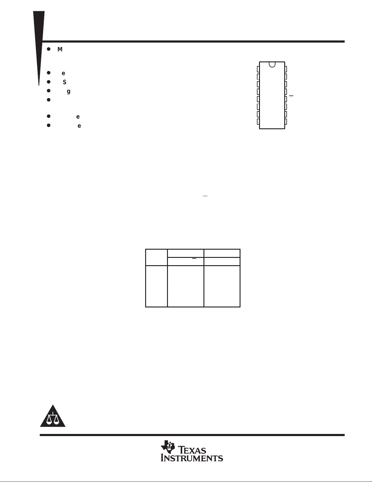
D OR N PACKAGE
(TOP VIEW)
1A
1
1Y
2
3
1Z
4
G
5
2Z
6
2Y
7
2A
8
GND
16
15
14
13
12
11
10
V
CC
4A
4Y
4Z
G
3Z
3Y
9
3A
description
The four differential line drivers are designed for data transmission over twisted-pair or parallel-wire
transmission lines. They meet the requirements of ANSI Standard EIA/TIA-422-B and ITU
Recommendations V.11 and are compatible with 3-state TTL circuits. Advanced low-power Schottky
technology provides high speed without the usual power penalties. Standby supply current is typically only
26 mA, while typical propagation delay time is less than 10 ns.
High-impedance inputs maintain low input currents, less than 1 µA for a high level and less than 100 µA for a
low level. Complementary output-enable inputs (G and G
input level or low input level. The SN75ALS192 is capable of data rates in excess of 20 Mbit/s and is designed
to operate with the SN75ALS193 quadruple line receiver.
The SN75ALS192 is characterized for operation from 0°C to 70°C.
) allow these devices to be enabled at either a high
FUNCTION TABLE
(each driver)
INPUT
A
H H X H L
L H XLH
H XLHL
L XLLH
X LHZZ
H = high level, L = low level, X = irrelevant,
Z = high impedance (off)
Please be aware that an important notice concerning availability, standard warranty, and use in critical applications of
Texas Instruments semiconductor products and disclaimers thereto appears at the end of this data sheet.
ENABLES OUTPUTS
G G Y Z
PRODUCTION DATA information is current as of publication date.
Products conform to specifications per the terms of Texas Instruments
standard warranty. Production processing does not necessarily include
testing of all parameters.
POST OFFICE BOX 655303 • DALLAS, TEXAS 75265
Copyright 1998, Texas Instruments Incorporated
1
Page 2
SN75ALS192
QUADRUPLE DIFFERENTIAL LINE DRIVER
SLLS007D – JULY 1985 – REVISED APRIL 1998
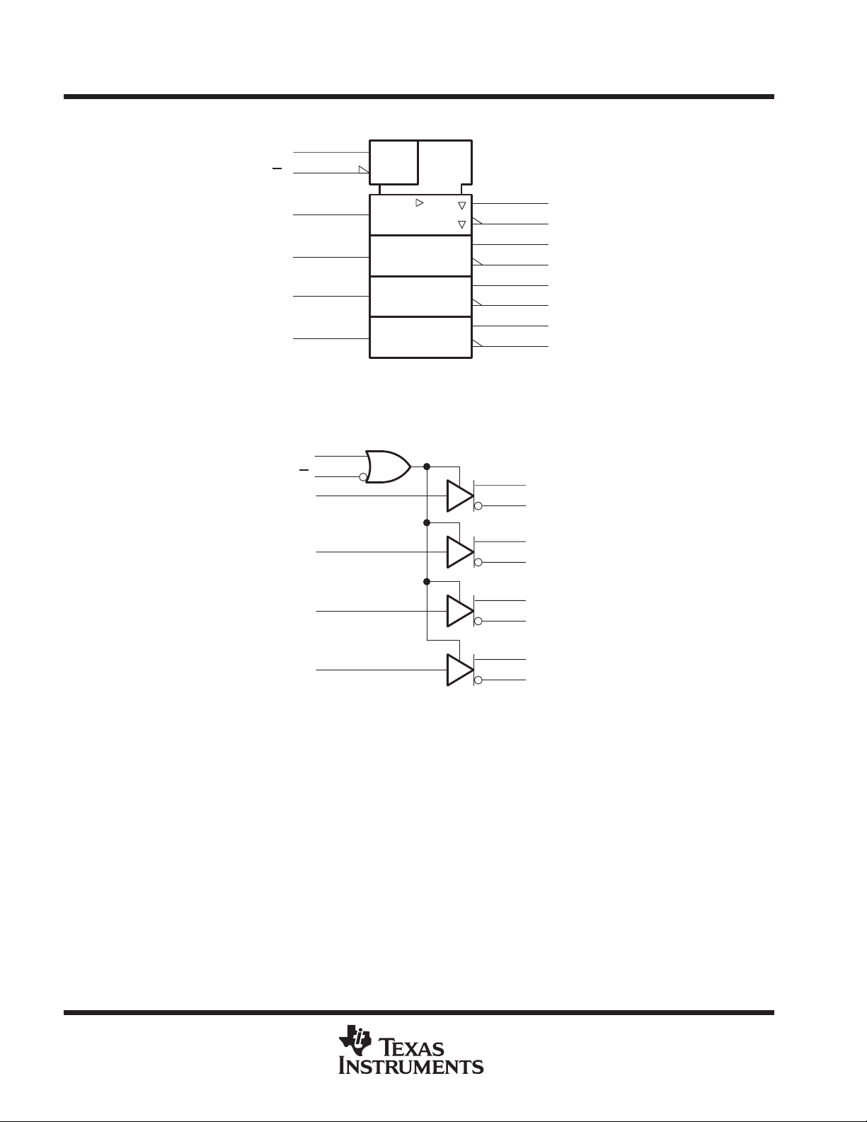
logic symbol
†
This symbol is in accordance with ANSI/IEEE Std 91-1984 and IEC Publication 617-12.
†
1A
2A
3A
4A
4
G
12
G
1
7
9
15
≥1
EN
logic diagram (positive logic)
4
G
12
G
1
1A
2
1Y
3
1Z
6
2Y
5
2Z
10
3Y
11
3Z
14
4Y
13
4Z
2
1Y
3
1Z
2A
3A
4A
7
9
15
10
11
14
13
6
2Y
5
2Z
3Y
3Z
4Y
4Z
2
POST OFFICE BOX 655303 • DALLAS, TEXAS 75265
Page 3
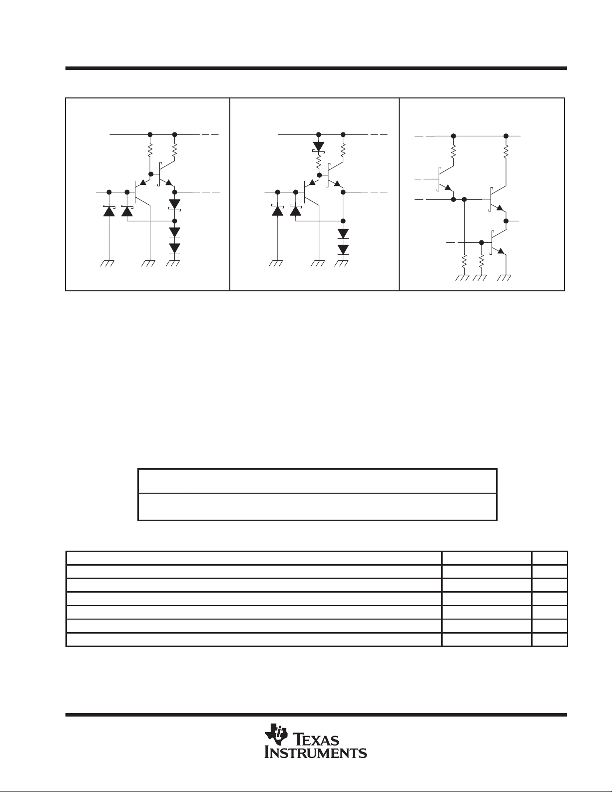
schematics of inputs and outputs
SN75ALS192
QUADRUPLE DIFFERENTIAL LINE DRIVER
SLLS007D – JULY 1985 – REVISED APRIL 1998
EQUIVALENT OF
EACH DATA (A) INPUT
V
CC
Input
Input
EQUIVALENT OF
EACH ENABLE INPUT
V
CC
EQUIVALENT OF
EACH OUTPUT
V
CC
Output
absolute maximum ratings over operating free-air temperature range (unless otherwise noted)
Supply voltage, V
Input voltage, V
Off-state output voltage 6 V. . . . . . . . . . . . . . . . . . . . . . . . . . . . . . . . . . . . . . . . . . . . . . . . . . . . . . . . . . . . . . . . . . . . . .
Continuous total dissipation See Dissipation Rating Table. . . . . . . . . . . . . . . . . . . . . . . . . . . . . . . . . . . . . . . . . . .
Storage temperature range, T
Lead temperature 1,6 mm (1/16 inch) from case for 10 seconds 260°C. . . . . . . . . . . . . . . . . . . . . . . . . . . . . . .
†
Stresses beyond those listed under “absolute maximum ratings” may cause permanent damage to the device. These are stress ratings only, and
functional operation of the device at these or any other conditions beyond those indicated under “recommended operating conditions” is not
implied. Exposure to absolute-maximum-rated conditions for extended periods may affect device reliability.
NOTE 1: All voltage values except differential output voltage, V
(see Note 1) 7 V. . . . . . . . . . . . . . . . . . . . . . . . . . . . . . . . . . . . . . . . . . . . . . . . . . . . . . . . . . . . .
CC
7 V. . . . . . . . . . . . . . . . . . . . . . . . . . . . . . . . . . . . . . . . . . . . . . . . . . . . . . . . . . . . . . . . . . . . . . . . . . . .
I
–65°C to 150°C. . . . . . . . . . . . . . . . . . . . . . . . . . . . . . . . . . . . . . . . . . . . . . . . . . .
stg
are with respect to network ground terminal.
OD,
†
PACKAGE
D 950 mW 7.6 mW/°C 608 mW N/A
N 1150 mW 9.2 mW/°C 736 mW N/A
TA ≤ 25°C
POWER RATING
recommended operating conditions
Supply voltage, V
High level input voltage, V
Low-level input voltage, V
High-level output current, I
Low-level output current, I
Operating free-air temperature, T
CC
IH
IL
OH
OL
A
DISSIPATION RATING TABLE
DERATING FACTOR
ABOVE TA = 25°C
POWER RATING
TA = 70°C
TA = 125°C
POWER RATING
MIN NOM MAX
4.75 5 5.25 V
2 V
0 70 °C
UNIT
0.8 V
–20 mA
20 mA
POST OFFICE BOX 655303 • DALLAS, TEXAS 75265
3
Page 4
SN75ALS192
IOOutput current with power off
V
0
A
IOZOff-state (high-impedance state) output current
V
MAX
A
QUADRUPLE DIFFERENTIAL LINE DRIVER
SLLS007D – JULY 1985 – REVISED APRIL 1998
electrical characteristics over recommended operating free-air temperature range (unless
otherwise noted)
PARAMETER
V
IK
V
OH
V
OL
V
O
|V
OD1
|V
OD2
∆|VOD|
V
OC
∆|VOC|
I
I
I
IH
I
IL
I
OS
I
CC
†
For conditions shown as MIN or MAX, use the appropriate value specified under recommended operating conditions.
‡
All typical values are at VCC = 5 V and TA = 25°C.
§
The minimum V
¶
|VOD| and |VOC| are the changes in magnitude of VOD and VOC, respectively, that occur when the input is changed from a high level to a low level.
#
In ANSI Standard EIA/TIA-422-B, VOC, which is the average of the two output voltages with respect to ground, is called output offset voltage,
VOS.
||
Not more than one output should be shorted at a time, and duration of the short circuit should not exceed one second.
Input clamp voltage VCC = MIN, II = –18 mA –1.5 V
High-level output voltage VCC = MIN, IOH = –20 mA 2.5 V
Low-level output voltage VCC = MIN, IOL = 20 mA 0.5 V
Output voltage VCC = MAX, IO = 0 0 6 V
| Differential output voltage VCC = MIN, IO = 0 1.5 6 V
| Differential output voltage RL = 100 Ω, See Figure 1 1/2 V
Change in magnitude of
differential output voltage
Common-mode output voltage
Change in magnitude of
common-mode output voltage
p
Input current at maximum input voltage VCC = MAX, VI = 7 V 100 µA
High-level input current VCC = MAX, VI = 2.7 V 20 µA
Low-level input current VCC = MAX, VI = 0.4 V –200 µA
Short-circuit output current
Supply current (all drivers) VCC = MAX, All outputs disabled 26 45 mA
with a 100-Ω load is either 1/2 V
OD2
¶
#
¶
p
p
||
p
or 2 V, whichever is greater.
OD1
TEST CONDITIONS
RL = 100 Ω, See Figure 1 ±0.2 V
RL = 100 Ω, See Figure 1 ±3 V
RL = 100 Ω, See Figure 1 ±0.2 V
=
CC
=
CC
VCC = MAX –30 –150 mA
VO = 6 V 100
VO = –0.25 V –100
VO = 0.5 V –20
VO = 2.5 V 20
†
MIN TYP‡MAX UNIT
§
or 2
OD1
µ
µ
V
switching characteristics, VCC = 5 V, TA = 25°C (see Figure 2)
PARAMETER TEST CONDITIONS MIN TYP MAX UNIT
t
PLH
t
PHL
t
PZH
t
PZL
t
PHZ
t
PLZ
Propagation delay time, low-to-high-Ievel output S1 and S2 open, CL = 30 pF 6 13 ns
Propagation delay time, high-to-low-level output S1 and S2 open, CL = 30 pF 9 14 ns
Output-to-output skew S1 and S2 open, CL = 30 pF 3 6 ns
Output enable time to high level S1 open and S2 closed 11 15 ns
Output enable time to low level S1 closed and S2 open 16 20 ns
Output disable time from high level S1 open and S2 closed, CL = 10 pF 8 15 ns
Output disable time from low level S1 and S2 closed, CL = 10 pF 18 20 ns
4
POST OFFICE BOX 655303 • DALLAS, TEXAS 75265
Page 5
SN75ALS192
QUADRUPLE DIFFERENTIAL LINE DRIVER
SLLS007D – JULY 1985 – REVISED APRIL 1998
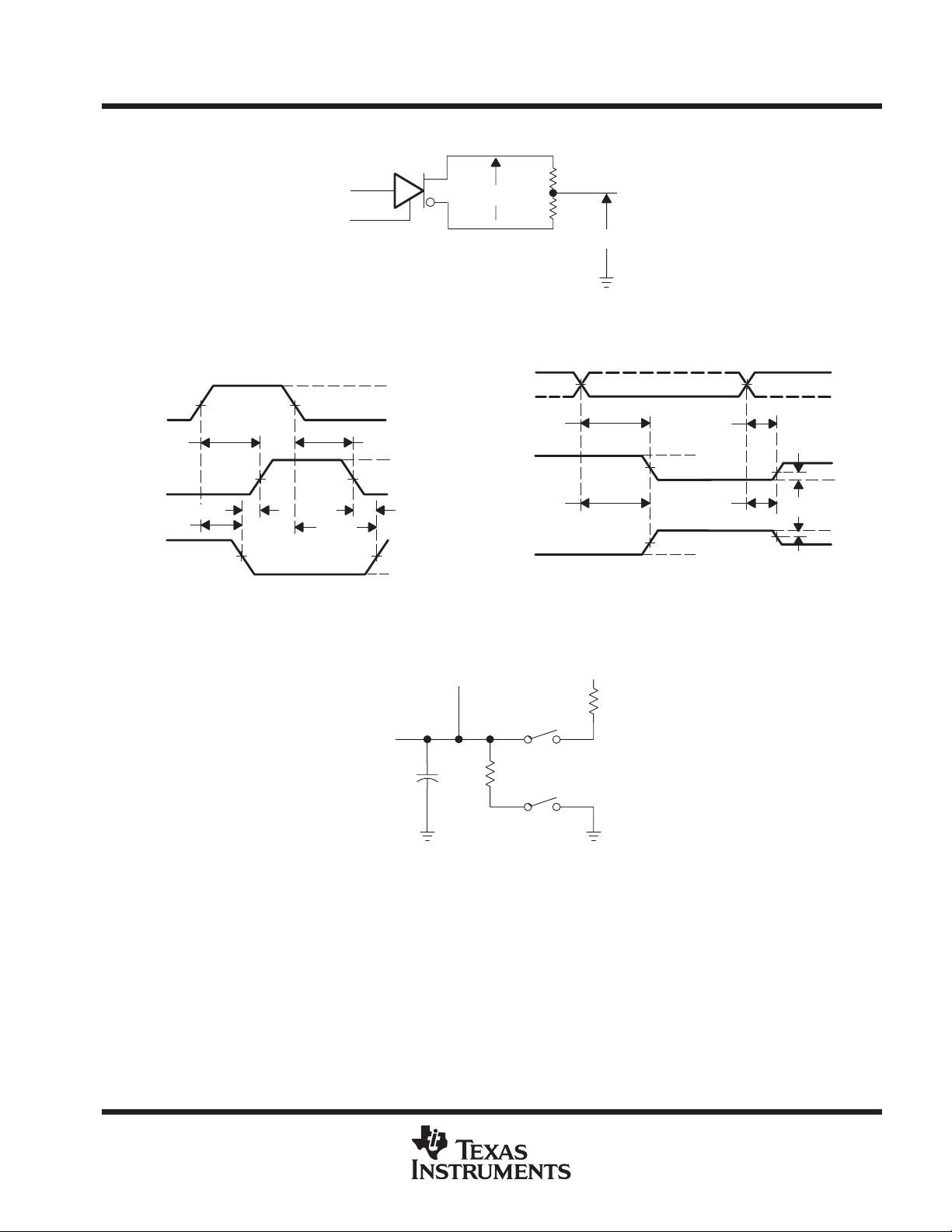
PARAMETER MEASUREMENT INFORMATION
Figure 1. Differential and Common-Mode Output Voltages
Input A
t
(see Note A)
Output Y
Output Z
PLH
t
PROPAGATION DELAY TIMES AND SKEW
1.3 V
1.5 V
Skew Skew
PHL
1.5 V 1.5 V
1.3 V
t
PLH
t
PHL
1.5 V
V
OD2
3 V
0 V
V
OH
V
OL
V
OH
V
OL
VOLTAGE WAVEFORMS
Enable G
Enable G
Waveform 1
(see Note C)
Waveform 2
(see Note C)
t
PZL
t
PZH
50 Ω
50 Ω
V
OC
See Note B
1.5 V
t
PLZ
≈ 4.5 V
S1 Closed
S2 Open
S1 Open
S2 Closed
ENABLE AND DISABLE TIMES
1.5 V
1.5 V
t
PHZ
≈ 0 V
1.5 V
S1 Closed
S2 Closed
0.5 V
0.5 V
S1 Closed
S2 Closed
3 V
0 V
≈ 1.5 V
V
OL
V
OH
≈ 1.5 V
Test
Point
From Output
Under Test
C
(see Note D)
NOTES: A. When measuring propagation delay times and skew, switches S1 and S2 are open.
B. Each enable is tested separately.
C. Waveform 1 is for an output with internal conditions such that the output is low except when disabled by the output control.
Waveform 2 is for an output with internal conditions such that the output is high except when disabled by the output control.
D. CL includes probe and jig capacitance.
E. All input pulses are supplied by generators having the following characteristics: PRR ≤ 1 MHz, ZO ≈ 50 Ω, tr ≤ 15 ns, and tf ≤ 6 ns.
L
TEST CIRCUIT
75 Ω
S1
S2
V
CC
180 Ω
Figure 2. Test Circuit and Voltage Waveforms
POST OFFICE BOX 655303 • DALLAS, TEXAS 75265
5
Page 6
SN75ALS192
QUADRUPLE DIFFERENTIAL LINE DRIVER
SLLS007D – JULY 1985 – REVISED APRIL 1998
5
No Load
Outputs Enabled
4.5
TA = 25°C
4
3.5
3
2.5
2
– Y Output Voltage – VV
O
1.5
1
0.5
0
0 0.5 1 1.5
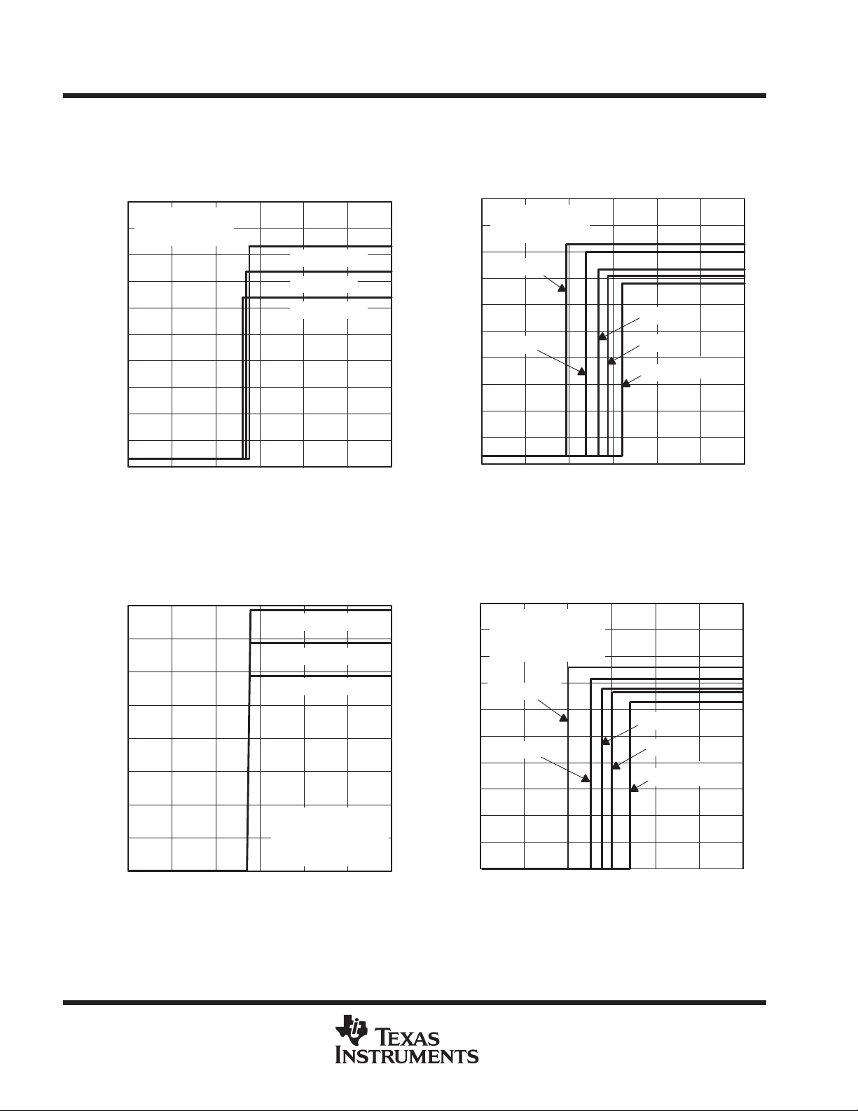
TYPICAL CHARACTERISTICS
Y OUTPUT VOLTAGE
vs
DATA INPUT VOLTAGE
VCC = 5.5 V
VCC = 5 V
VCC = 4.5 V
2 2.5 3
VI – Data Input Voltage – V
Figure 3
†
5
VCC = 5 V
Outputs Enabled
4.5
No Load
4
TA = 125°C
3.5
3
2.5
TA = 70°C
2
– Y Output Voltage – VV
O
1.5
1
0.5
0
0 0.5 1 1.5
Y OUTPUT VOLTAGE
vs
DATA INPUT VOLTAGE
TA = 25°C
TA = 0°C
TA = –55°C
2 2.5 3
VI – Data Input Voltage – V
Figure 4
Y OUTPUT VOLTAGE
vs
ENABLE G INPUT VOLTAGE
4
3.5
3
2.5
2
1.5
– Y Output Voltage – VV
O
1
0.5
0
0 0.5 1 1.5 2
VI – Enable G Input Voltage – V
NOTE A: The A input is connected to VCC during the testing of the
Y outputs and to ground during the testing of the Z outputs.
VCC = 5.5 V
VCC = 5 V
VCC = 4.5 V
VI = 2 V
RL = 470 Ω to GND
See Note A
TA = 25°C
2.5 3
NOTE A: The A input is connected to VCC during the testing of the
5
VCC = 5 V
VI = 2 V
4.5
RL = 470 Ω to GND
4
See Note A
3.5
TA = 125°C
3
2.5
– Y Output Voltage – VV
O
1.5
0.5
TA = 70°C
2
1
0
0 0.5 1 1.5
Y outputs and to ground during the testing of the Z outputs.
Figure 5
†
Operation of the device at these or any other conditions beyond those indicated under “recommended operating conditions” is not implied.
Y OUTPUT VOLTAGE
vs
ENABLE G INPUT VOLTAGE
TA = 25°C
TA = 0°C
TA = –55°C
2 2.5 3
VI – Enable G Input Voltage – V
Figure 6
6
POST OFFICE BOX 655303 • DALLAS, TEXAS 75265
Page 7
SN75ALS192
QUADRUPLE DIFFERENTIAL LINE DRIVER
SLLS007D – JULY 1985 – REVISED APRIL 1998
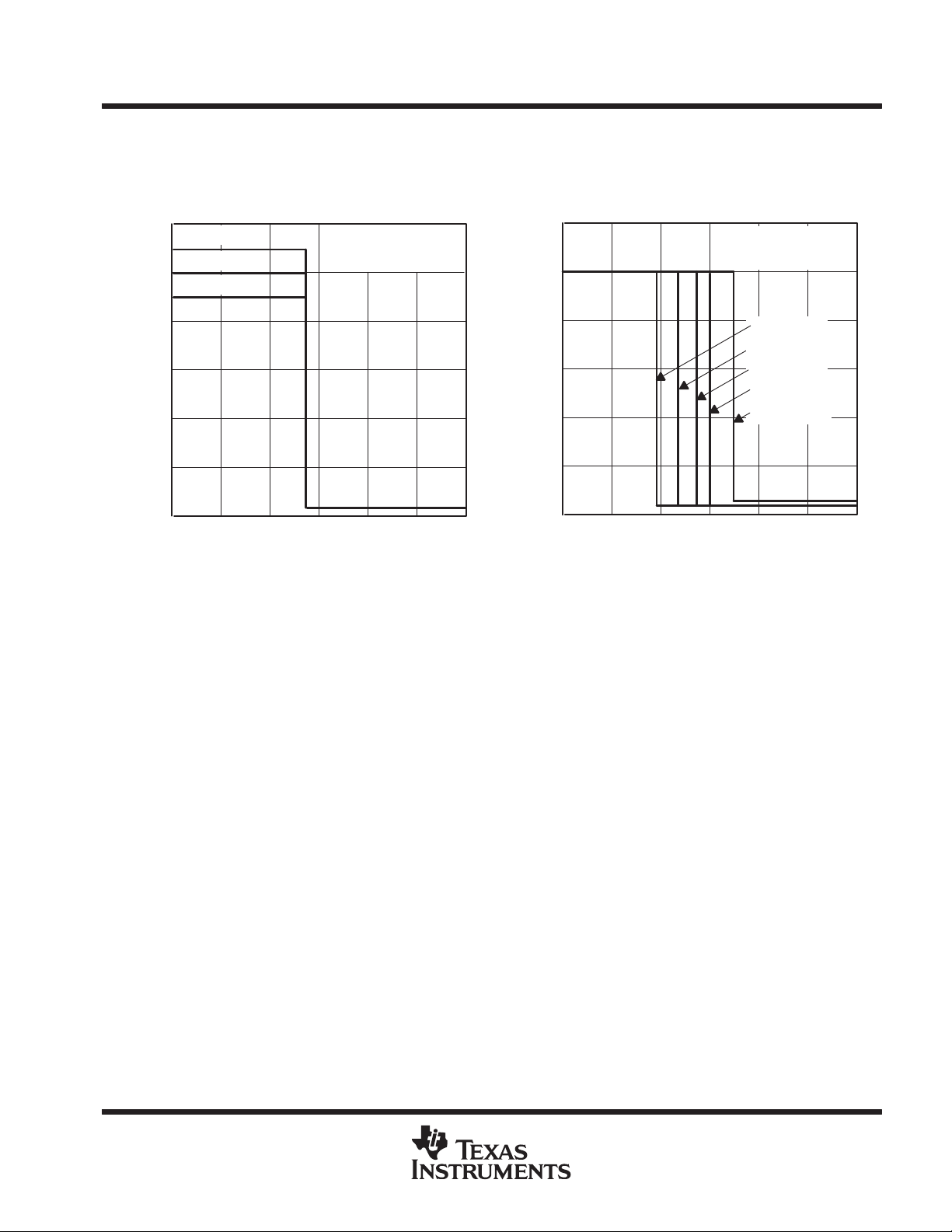
TYPICAL CHARACTERISTICS
Z OUTPUT VOLTAGE
vs
ENABLE G INPUT VOLTAGE
6
VCC = 5.5 V
VCC = 5 V
5
VCC = 4.5 V
4
3
2
– Y Output Voltage – VV
O
1
0
0 0.5 1
VI – Enable G Input Voltage – V
NOTE A: The A input is connected to VCC during the testing of the
Y outputs and to ground during the testing of the Z outputs.
RL = 470 Ω to V
See Note A
TA = 25°C
1.5 2 2.5 3
CC
†
Z OUTPUT VOLTAGE
vs
ENABLE G INPUT VOLTAGE
6
5
4
3
2
– Y Output Voltage – VV
O
1
0
0 0.5 1
VI – Enable G Input Voltage – V
NOTE B: The A input is connected to GND during the testing of the
Y outputs and to VCC during the testing of the Z outputs.
VCC = 5 V
RL = 470 Ω to V
See Note B
TA = 125°C
TA = 70°C
TA = 25°C
TA = 0°C
TA = –55°C
1.5 2 2.5 3
CC
Figure 7
†
Operation of the device at these or any other conditions beyond those indicated under “recommended operating conditions” is not implied.
Figure 8
POST OFFICE BOX 655303 • DALLAS, TEXAS 75265
7
Page 8
SN75ALS192
QUADRUPLE DIFFERENTIAL LINE DRIVER
SLLS007D – JULY 1985 – REVISED APRIL 1998
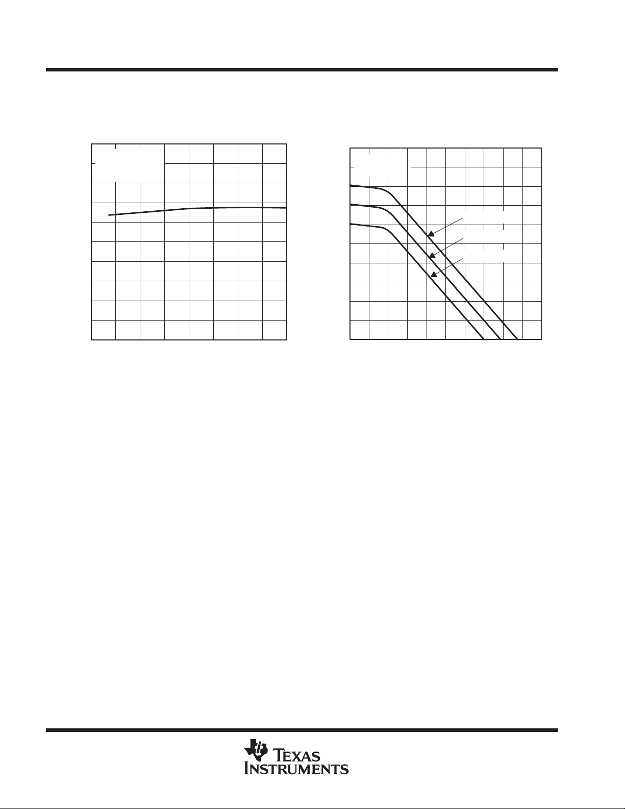
TYPICAL CHARACTERISTICS
HIGH-LEVEL OUTPUT VOLTAGE
vs
5
4.5
4
3.5
3
2.5
2
1.5
– High-Level Output Voltage – VV
OH
1
0.5
0
– 75 –50 – 25 0 25 50
NOTE A: The A input is connected to VCC during the testing of the
†
Operation of the device at these or any other conditions beyond those indicated under “recommended operating conditions” is not implied.
Y outputs and to ground during the testing of the Z outputs.
FREE-AIR TEMPERATURE
VCC = 5 V
IOH = –20 mA
See Note A
TA – Free-Air Temperature – ° C
Figure 9
75 100 125
5
4.5
4
3.5
3
2.5
2
1.5
– High-Level Output Voltage – VV
OH
1
0.5
0
NOTE A: The A input is connected to VCC during the testing of the
†
HIGH-LEVEL OUTPUT VOLTAGE
vs
OUTPUT CURRENT
See Note A
TA = 25°C
VCC = 5.5 V
VCC = 5 V
VCC = 4.5 V
0 – 20 – 40 – 60 – 80 – 100
IOH – High-Level Output Current – mA
Y outputs and to ground during the testing of the Z outputs.
Figure 10
8
POST OFFICE BOX 655303 • DALLAS, TEXAS 75265
Page 9
SN75ALS192
QUADRUPLE DIFFERENTIAL LINE DRIVER
SLLS007D – JULY 1985 – REVISED APRIL 1998
TYPICAL CHARACTERISTICS
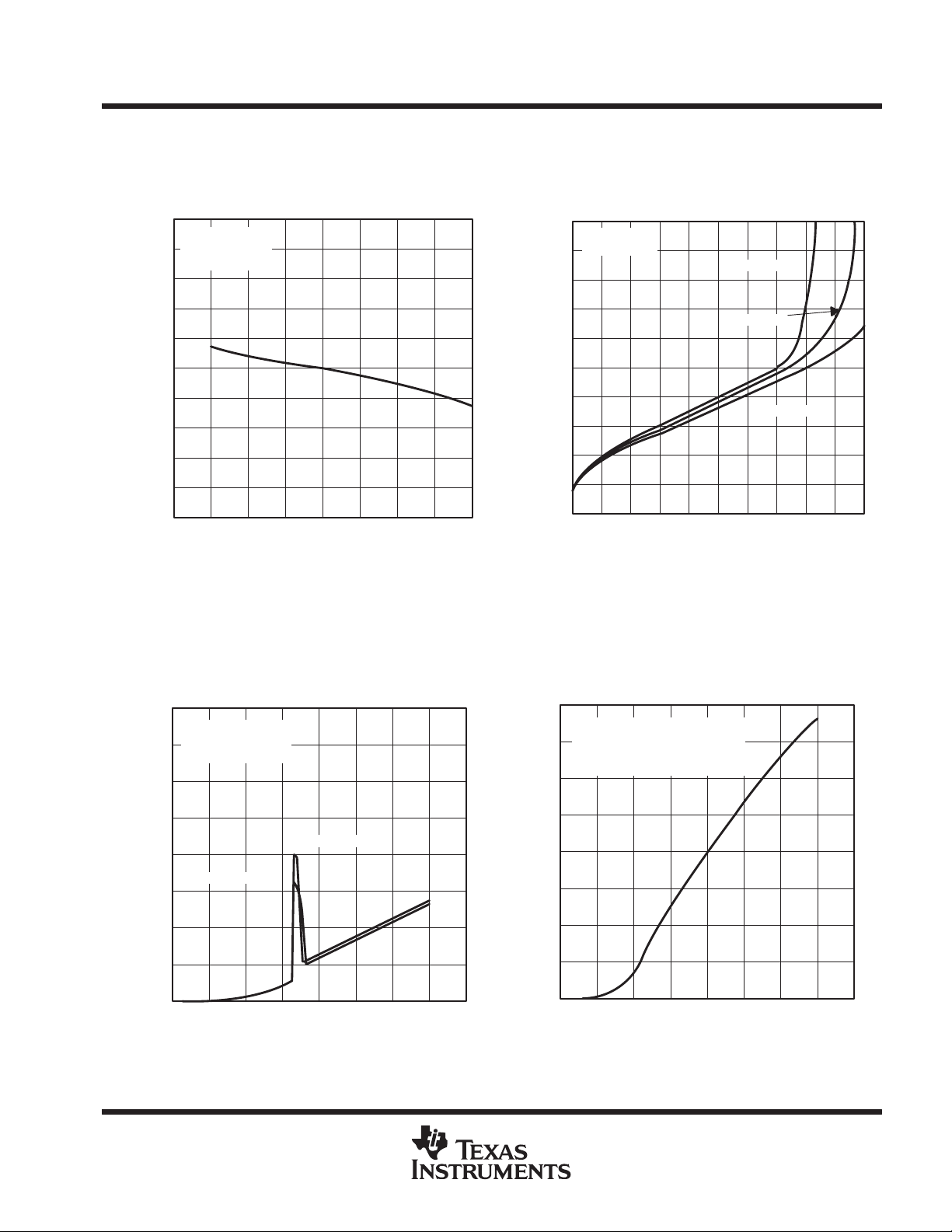
LOW-LEVEL OUTPUT VOLTAGE
vs
FREE-AIR TEMPERATURE
0.5
VCC = 5 V
IOL= –20 mA
0.45
See Note A
0.4
0.35
0.3
0.25
0.2
0.15
– Low-Level Output Voltage – VV
OL
0.1
0.05
0
– 75 – 50 – 25 0 25 50 75 100 125
TA – Free-Air Temperature – ° C
NOTE A: The A input is connected to GND during the testing of the
Y outputs and to VCC during the testing of the Z outputs.
Figure 11
†
LOW-LEVEL OUTPUT VOLTAGE
vs
LOW-LEVEL OUTPUT CURRENT
1
See Note A
TA = 25°C
0.9
0.8
0.7
0.6
0.5
0.4
0.3
– Low-Level Output Voltage – VV
OL
0.2
0.1
0
02040608010010 30 50 70 90
IOL – Low-Level Output Current – mA
NOTE A: The A input is connected to GND during the testing of the
Y outputs and to VCC during the testing of the Z outputs.
VCC = 4.5 V
VCC = 5 V
VCC = 5.5 V
Figure 12
SUPPLY CURRENT
vs
80
SUPPLY VOLTAGE
Outputs Enabled
No Load
70
TA = 25°C
60
50
Inputs Grounded
40
Inputs Open
30
– Supply Current – mAI
CC
20
10
0
012345
VCC – Supply Voltage– V
678
40
A Inputs Open or Grounded
Outputs Disabled
35
No Load
TA = 25°C
30
25
20
15
– Supply Current – mAI
CC
10
5
0
012345
Figure 13
†
Operation of the device at these or any other conditions beyond those indicated under “recommended operating conditions” is not implied.
SUPPLY CURRENT
vs
SUPPLY VOLTAGE
678
VCC – Supply Voltage – V
Figure 14
POST OFFICE BOX 655303 • DALLAS, TEXAS 75265
9
Page 10
SN75ALS192
QUADRUPLE DIFFERENTIAL LINE DRIVER
SLLS007D – JULY 1985 – REVISED APRIL 1998
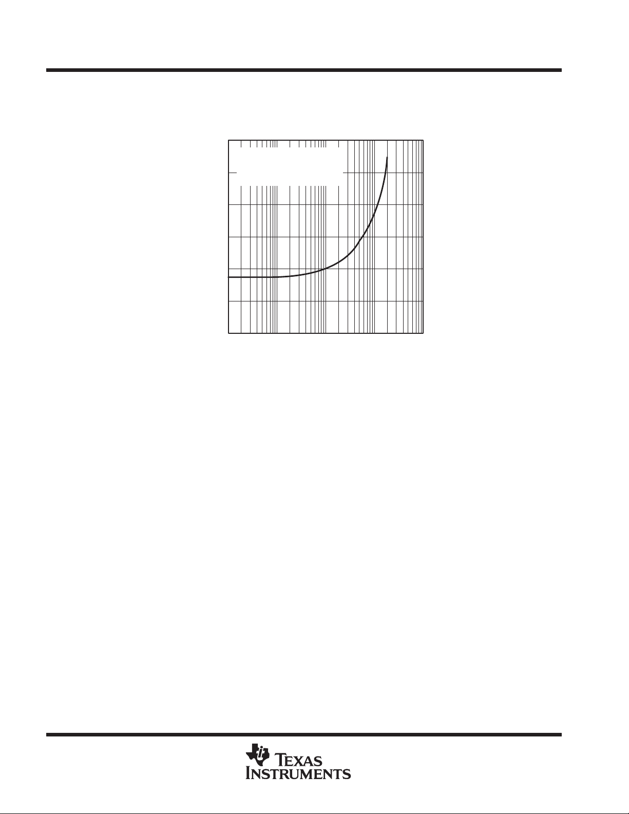
TYPICAL CHARACTERISTICS
60
VCC = 5 V
Input = 0 to 3 V
Duty Cycle = 50%
50
CL = 30 pF to All Outputs
40
30
20
– Supply Current – mAI
CC
10
SUPPLY CURRENT
vs
FREQUENCY
0
10 k 100 k 1 M 10 M 100 M
f – Frequency– Hz
Figure 15
10
POST OFFICE BOX 655303 • DALLAS, TEXAS 75265
Page 11

IMPORTANT NOTICE
T exas Instruments and its subsidiaries (TI) reserve the right to make changes to their products or to discontinue
any product or service without notice, and advise customers to obtain the latest version of relevant information
to verify, before placing orders, that information being relied on is current and complete. All products are sold
subject to the terms and conditions of sale supplied at the time of order acknowledgement, including those
pertaining to warranty, patent infringement, and limitation of liability.
TI warrants performance of its semiconductor products to the specifications applicable at the time of sale in
accordance with TI’s standard warranty. Testing and other quality control techniques are utilized to the extent
TI deems necessary to support this warranty . Specific testing of all parameters of each device is not necessarily
performed, except those mandated by government requirements.
CERT AIN APPLICATIONS USING SEMICONDUCTOR PRODUCTS MAY INVOLVE POTENTIAL RISKS OF
DEATH, PERSONAL INJURY, OR SEVERE PROPERTY OR ENVIRONMENTAL DAMAGE (“CRITICAL
APPLICATIONS”). TI SEMICONDUCTOR PRODUCTS ARE NOT DESIGNED, AUTHORIZED, OR
WARRANTED TO BE SUITABLE FOR USE IN LIFE-SUPPORT DEVICES OR SYSTEMS OR OTHER
CRITICAL APPLICA TIONS. INCLUSION OF TI PRODUCTS IN SUCH APPLICATIONS IS UNDERST OOD TO
BE FULLY AT THE CUSTOMER’S RISK.
In order to minimize risks associated with the customer’s applications, adequate design and operating
safeguards must be provided by the customer to minimize inherent or procedural hazards.
TI assumes no liability for applications assistance or customer product design. TI does not warrant or represent
that any license, either express or implied, is granted under any patent right, copyright, mask work right, or other
intellectual property right of TI covering or relating to any combination, machine, or process in which such
semiconductor products or services might be or are used. TI’s publication of information regarding any third
party’s products or services does not constitute TI’s approval, warranty or endorsement thereof.
Copyright 1998, Texas Instruments Incorporated
 Loading...