

Page 1
SN55ALS161, SN75ALS161
OCTAL GENERAL-PURPOSE INTERFACE BUS TRANSCEIVERS
SLLS019E – JUNE 1986 – REVISED NOVEMBER 1999
SUITABLE FOR IEEE STANDARD 488-1978 (GPIB)
D
8-Channel Bidirectional Transceivers
D
Designed to Implement Control Bus
Interface
D
Designed for Single Controller
D
High-Speed Advanced Low-Power Schottky
Circuitry
D
Low Power Dissipation:
SN55ALS161 . . . 59 mW Max Per Channel
SN75ALS161 . . . 46 mW Max Per Channel
D
Fast Propagation Times:
SN55ALS161 . . . 25 ns Max
SN75ALS161 . . . 20 ns Max
D
High-Impedance pnp Inputs
D
Receiver Hysteresis:
SN55ALS161 . . . 550 mV Typ
SN75ALS161 . . . 650 mV Typ
D
Bus-Terminating Resistors Provided on
Driver Outputs
D
No Loading of Bus When Device Is
Powered Down (VCC = 0)
D
Power-Up/Power-Down Protection
(Glitch Free)
description
GPIB
I/O Ports
†
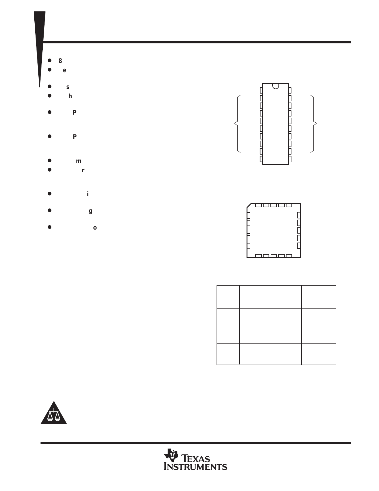
SN55ALS161 . . . J OR W PACKAGE
SN75ALS161 . . . DW OR N PACKAGE
(TOP VIEW)
TE
20
19
18
17
16
15
14
13
12
11
CC
V
V
CC
REN
IFC
NDAC
NRFD
DAV
EOI
ATN
SRQ
DC
REN
18
17
16
15
14
IFC
NDAC
NRFD
DAV
EOI
TE
1
REN
NDAC
NRFD
DAV
SRQ
GND
SN55ALS161 . . . FK PACKAGE
NDAC
NRFD
DAV
EOI
ATN
2
IFC
3
4
5
6
7
EOI
8
ATN
9
10
(TOP VIEW)
IFC
REN
3212019
4
5
6
7
8
910111213
Terminal
I/O Ports
The SN55ALS161 and SN75ALS161
eight-channel general-purpose interface bus
transceivers are high-speed, advanced
low-power Schottky-process devices designed to
provide the bus-management and data-transfer
signals between operating units of a
single-controller instrumentation system. When
combined with the SN55ALS160 and
SN75ALS160 octal bus transceivers, these
devices provide a complete 16-wire interface for
the IEEE 488 bus.
The SN55ALS161 and SN75ALS161 devices
feature eight driver-receiver pairs connected in a
front-to-back configuration to form input/output
CHANNEL-IDENTIFICATION TABLE
NAME CLASSIDENTITY
DC
TE
ATN
SRQ
REN
IFC
EOI
DAV
NDAC
NRFD
Direction Control
Talk Enable
Attention
Service Request
Remote Enable
Interface Clear
End or Identify
Data Valid
Not Data Accepted
Not Ready for Data
SRQ
GND
DC
SRQ
ATN
Control
Bus
Management
Data
Transfer
(I/O) ports at both the bus and terminal sides. The
direction of data through these driver-receiver
pairs is determined by the direction-control (DC)
and talk-enable (TE) signals.
Please be aware that an important notice concerning availability, standard warranty, and use in critical applications of
Texas Instruments semiconductor products and disclaimers thereto appears at the end of this data sheet.
†
The transceivers are suitable for IEEE Standard 488 applications to the extent of the operating conditions and characteristics specified in this
data sheet. Certain limits contained in the IEEE specification are not met or cannot be tested over the entire military temperature range.
PRODUCTION DATA information is current as of publication date.
Products conform to specifications per the terms of Texas Instruments
standard warranty. Production processing does not necessarily include
testing of all parameters.
Copyright 1999, Texas Instruments Incorporated
On products compliant to MIL-PRF-38535, all parameters are tested
unless otherwise noted. On all other products, production
processing does not necessarily include testing of all parameters.
POST OFFICE BOX 655303 • DALLAS, TEXAS 75265
1
Page 2
SN55ALS161, SN75ALS161
RTR
RRTRR
TRT
TTRTT
OCTAL GENERAL-PURPOSE INTERFACE BUS TRANSCEIVERS
SLLS019E – JUNE 1986 – REVISED NOVEMBER 1999
description (continued)
The driver outputs general-purpose interface bus (GPIB I/O ports) feature active bus-terminating resistor
circuits designed to provide a high impedance to the bus when VCC = 0. The drivers are designed to handle
sink-current loads up to 48 mA. Each receiver features pnp transistor inputs for high input impedance and
hysteresis of 400 mV on the commercial part, 250 mV on the military part, minimum, for increased noise
immunity. All receivers have 3-state outputs to present a high impedance to the terminal when disabled.
The SN55ALS161 is characterized for operation over the full military temperature range of –55°C to 125°C. The
SN75ALS161 is characterized for operation from 0°C to 70°C.
FUNCTION TABLE
RECEIVE/TRANSMIT
CONTROLS
DC TE ATN†ATN†SRQ REN IFC EOI DAV NDAC NRFD
H H H
H H L
L L H
L L L
H L X R T R R R R T T
L H X T R T T T T R R
H = high level, L = low level, R = receive, T = transmit, X = irrelevant
Direction of data transmission is from the terminal side to the bus side, and the direction of data receiving
is from the bus side to the terminal side.
Data transfer is noninverting in both directions.
†
ATN is a normal transceiver channel that functions additionally as an internal direction control or talk
enable for EOI whenever the DC and TE inputs are in the same state. When DC and TE are in opposite
states, the ATN channel functions as an independent transceiver only.
BUS-MANAGEMENT CHANNELS DATA-TRANSFER CHANNELS
(CONTROLLED BY DC) (CONTROLLED BY TE)
T
R
2
POST OFFICE BOX 655303 • DALLAS, TEXAS 75265
Page 3
SN55ALS161, SN75ALS161
OCTAL GENERAL-PURPOSE INTERFACE BUS TRANSCEIVERS
SLLS019E – JUNE 1986 – REVISED NOVEMBER 1999
11
1
13
19
18
15
17
16
†
EN1/G4
EN2/G5
≥ 1
5
4
1
11
11
2
2
2
EN3
8
1
11
3
13
1
1
1
1
2
1
2
1
2
1
ATN
714
EOI
912
SRQ
2
REN
3
IFC
6
DAV
4
NDAC
5
NRFD
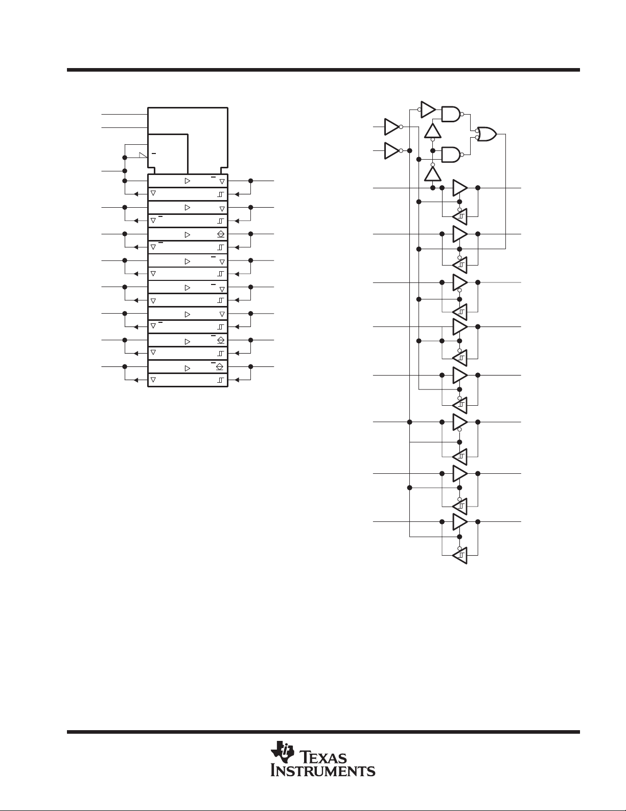
logic symbol
DC
TE
ATN
EOI
SRQ
REN
IFC
DAV
NDAC
NRFD
†
This symbol is in accordance with ANSI/IEEE Std 91-1984 and
IEC Publication 617-12.
logic diagram (positive logic)
11
DC
1
TE
13
ATN
14
EOI
12
SRQ
19
REN
18
IFC
15
DAV
8
ATN
7
EOI
9
SRQ
2
REN
3
IFC
6
DAV
NDAC
NRFD
17
16
4
5
NDAC
NRFD
POST OFFICE BOX 655303 • DALLAS, TEXAS 75265
3
Page 4
SN55ALS161, SN75ALS161
OCTAL GENERAL-PURPOSE INTERFACE BUS TRANSCEIVERS
SLLS019E – JUNE 1986 – REVISED NOVEMBER 1999
schematics of inputs and outputs
EQUIVALENT OF ALL CONTROL INPUTS TYPICAL OF SRQ, NDAC, AND NRFD GPIB I/O PORT
V
CC
9 kΩ
NOM
Input
GND
Input/Output Port
Circuit inside dashed lines is on the driver outputs only.
TYPICAL OF ALL I/O PORTS EXCEPT SRQ, NDAC, NRFD GPIB I/O PORTS
1.7 kΩ
NOM
4 kΩ
NOM
10 kΩ
NOM
R
(eq)
4 kΩ
NOM
Input/Output Port
Driver output R
Receiver output R
R
= equivalent resistor
(eq)
Circuit inside dashed lines is on the driver outputs only.
= 30 Ω NOM
(eq)
= 110 Ω NOM
(eq)
1.7 kΩ
NOM
4 kΩ
NOM
10 kΩ
NOM
4
POST OFFICE BOX 655303 • DALLAS, TEXAS 75265
Page 5
High-level output current, I
Low-level output current, I
mA
SN55ALS161, SN75ALS161
OCTAL GENERAL-PURPOSE INTERFACE BUS TRANSCEIVERS
SLLS019E – JUNE 1986 – REVISED NOVEMBER 1999
absolute maximum ratings over operating free-air temperature range (unless otherwise noted)
Supply voltage, VCC (see Note 1) 7 V. . . . . . . . . . . . . . . . . . . . . . . . . . . . . . . . . . . . . . . . . . . . . . . . . . . . . . . . . . . . .
Input voltage, VI 5.5 V. . . . . . . . . . . . . . . . . . . . . . . . . . . . . . . . . . . . . . . . . . . . . . . . . . . . . . . . . . . . . . . . . . . . . . . . . .
Low-level driver output current, I
Continuous total dissipation See Dissipation Rating Table. . . . . . . . . . . . . . . . . . . . . . . . . . . . . . . . . . . . . . . . . . .
Package thermal impedance, θJA (see Note 2): DW package 58°C/W. . . . . . . . . . . . . . . . . . . . . . . . . . . . . . . . .
Case temperature for 60 seconds: FK package, T
Lead temperature 1,6 mm (1/16 inch) from the case for 60 seconds: J or W package 300°C. . . . . . . . . . . . .
Lead temperature 1,6 mm (1/16 inch) from the case for 10 seconds: DW or N package 260°C. . . . . . . . . . .
Storage temperature range, T
†
Stresses beyond those listed under “absolute maximum ratings” may cause permanent damage to the device. These are stress ratings only, and
functional operation of the device at these or any other conditions beyond those indicated under “recommended operating conditions” is not
implied. Exposure to absolute-maximum-rated conditions for extended periods may affect device reliability.
NOTES: 1. All voltage values are with respect to network ground terminal.
2. The package thermal impedance is calculated in accordance with JESD 51.
PACKAGE
FK 1375 mW 11.0 mW/°C 880 mW 275 mW
J 1375 mW 11.0 mW/°C 880 mW 275 mW
W 1000 mW 8.0 mW/°C 640 mW 200 mW
POWER RATING
100 mA. . . . . . . . . . . . . . . . . . . . . . . . . . . . . . . . . . . . . . . . . . . . . . . . . . . . . . . .
OL
N package 69°C/W. . . . . . . . . . . . . . . . . . . . . . . . . . . . . . . . . . .
260°C. . . . . . . . . . . . . . . . . . . . . . . . . . . . . . . . . . . . . . . . . .
C
–65°C to 150°C. . . . . . . . . . . . . . . . . . . . . . . . . . . . . . . . . . . . . . . . . . . . . . . . . . .
stg
DISSIPATION RATING TABLE
TA ≤ 25°C
OPERATING
FACTOR
TA = 70°C
POWER RATING
TA = 125°C
POWER RATING
†
SN55ALS161 recommended operating conditions
Supply voltage, V
High-level input voltage, V
Low-level input voltage, V
Operating free-air temperature, T
CC
TE and DC at TA = –55°C to 125°C 2
IH
IL
p
p
OH
OL
A
Bus and terminal at TA = 25°C to 125°C 2
Bus and terminal at TA = –55°C 2.1
TE and DC at TA = –55°C to 125°C 0.8
Bus and terminal at TA = 25°C to –55°C 0.8
Bus and terminal at TA = 125°C 0.7
Bus ports with pullups active (VCC = 5 V) –5.2 mA
Terminal ports –800 µA
Bus ports 48
Terminal ports 16
MIN NOM MAX UNIT
4.75 5 5.25 V
V
V
–55 125 °C
POST OFFICE BOX 655303 • DALLAS, TEXAS 75265
5
Page 6

SN55ALS161, SN75ALS161
High-level output current, I
Low-level output current, I
mA
OCTAL GENERAL-PURPOSE INTERFACE BUS TRANSCEIVERS
SLLS019E – JUNE 1986 – REVISED NOVEMBER 1999
SN75ALS161 recommended operating conditions
Supply voltage, V
High-level input voltage, V
Low-level input voltage, V
Operating free-air temperature, T
CC
IH
IL
p
p
OH
OL
A
Bus ports with pullups active –5.2 mA
Terminal ports –800 µA
Bus ports 48
Terminal ports 16
MIN NOM MAX UNIT
4.75 5 5.25 V
2 V
0.8 V
0 70 °C
6
POST OFFICE BOX 655303 • DALLAS, TEXAS 75265
Page 7

PARAMETER
TEST CONDITIONS
†
UNIT
Hysteresis
y
Bus
OH
µ ,
CC
V
§
t
V
OH,CC
V
t
V
V
Voltage at GPIB I/O port
V
V
V
I/O
(SN55 )
I
§
t
V
MAX
mA
SN55ALS161, SN75ALS161
OCTAL GENERAL-PURPOSE INTERFACE BUS TRANSCEIVERS
SLLS019E – JUNE 1986 – REVISED NOVEMBER 1999
electrical characteristics over recommended ranges of supply voltage and operating free-air
temperature (unless otherwise noted)
SN55ALS161 SN75ALS161
MIN TYP‡MAX MIN TYP‡MAX
V
Input clamp voltage II = –18 mA –0.8 –1.5 –0.8 –1.5 V
IK
Bus 0.4 0.65
V
voltage
hys
(V
– V
IT+
High-level
p
outpu
OH
voltage
Low-level
p
outpu
OL
voltage
Input current
at maximum
I
I
input voltage
High-level
I
IH
input current
Low-level
I
IL
input current
I/O
Current into
GPIB I/O
I
port
Short-circuit
p
outpu
OS
current
I
Supply current No load,
CC
GPIB I/O port
C
I/O
capacitance
†
For conditions shown as MIN or MAX, use the appropriate value specified under recommended operating conditions.
‡
All typical values are at VCC = 5 V, TA = 25°C.
§
VOH and IOS apply to 3-state outputs only.
¶
For SN55’, IOL = 24 mA at –55°C.
)
IT–
Terminal I
Bus
Terminal IOL = 16 mA, VCC = MIN 0.3 0.5 0.3 0.5
Bus
Terminal VI = 5.5 V, VCC = MAX 0.2 100 0.2 100 µA
Terminal
and
control
inputs
Power
on
Power off VCC = 0 V
Terminal
Bus
VCC = 5 V, TA = –55°C and 25°C 0.4 0.55 V
VCC = 5 V, TA = 125°C 0.25
TA = 25°C
= – 800 µA, V
I
= – 5.2 mA, V
IOL = 48 mA¶, VCC = MIN 0.35 0.5 0.35 0.5
VI = 2.7 V, VCC = MAX 0.1 20 0.1 20 µA
VI = 0.5 V, VCC = MAX –30 –100 –10 –100 µA
Driver disabled,
p
= 5
CC
(SN55’)
Driver disabled,
VCC = 5 V
’
=
CC
VCC = 0 to 5 V, V
= MIN
= MIN
I
I(bus)
I
I(bus)
V
I(bus)
V
I(bus)
V
I(bus)
V
I(bus)
V
I(bus)
I(bus)
TE and DC low,
VCC = MAX
= 0 to 2 V, f = 1 MHz 30 30 pF
I/O
and MAX
TA = MIN 2.5 3.5 2.7 3.5
TA = 25°C
and MAX
TA = MIN 2.0 2.2
= 0 2.5 3 3.7 2.5 3 3.7
= –12 mA –1.5 –1.5
= –1.5 V to 0.4 V –1.3 –1.3
= 0.4 V to 2.5 V 0 –3.2 0 –3.2
= 2.5 V to 3.7 V
= 3.7 V to 5 V 0 2.5 0 2.5
= 5 V to 5.5 V 0.7 2.5 0.7 2.5
= 0 to 2.5 V 40 40 µA
2.7 3.5 2.7 3.5
2.2 2.2
2.5
–3.2
–15 –35 –75 –15 –35 –75
–25 –50 –125 –25 –50 –125
55 90 55 75 mA
2.5
–3.2
mA
POST OFFICE BOX 655303 • DALLAS, TEXAS 75265
7
Page 8

SN55ALS161, SN75ALS161
t
gy,
Terminal
SRQ, NDAC
and
)
See Figure 1
ns
t
gy
and NRFD)
t
gy,
Terminal
(,
See Figure 2
ns
t
gy,
t
gy,
Bus
Terminal
See Figure 2
ns
t
gy,
t
Output enable time to high level
t
g
TE or DC
REN, IFC
and
)
See Figure 3
ns
t
Output enable time to low level
and DAV)
t
t
Output enable time to high level
t
g
TE or DC
Bus (EOI)
See Figure 3
ns
t
Output enable time to low level
t
t
Output enable time to high level
t
g
TE or DC
Terminal
See Figure 4
ns
t
Output enable time to low level
t
OCTAL GENERAL-PURPOSE INTERFACE BUS TRANSCEIVERS
SLLS019E – JUNE 1986 – REVISED NOVEMBER 1999
SN55ALS161 switching characteristics, V
PARAMETER
Propagation delay time,
PLH
low- to high-level output
Propagation delay time,
PHL
high- to low-level output
Propagation delay time,
PLH
low- to high-level output
Propagation delay time,
PHL
high- to low-level output
Propagation delay time,
PLH
low- to high-level output
Propagation delay time,
PHL
high- to low-level output
PZH
PHZ
PZL
PLZ
PZH
PHZ
PZL
PLZ
PZH
PHZ
PZL
PLZ
†
Full range is –55°C to 125°C.
‡
All typical values are at VCC = 5 V.
p
Output disable time from high
level
p
Output disable time from low
level
p
Output disable time from high
level
p
Output disable time from low
level
p
Output disable time from high
level
p
Output disable time from low
level
FROM
(INPUT)
,
= 5 V and CL = 50 pF (unless otherwise noted)
CC
TO
(OUTPUT)
Bus (Except
,
NRFD
Bus (NRFD,
SRQ, NDAC)
Bus (ATN,
,
DAV
TEST
CONDITIONS
†
T
A
25°C 10 17
Full range 20
25°C 10 14
Full range 18
25°C 25
Full range 37
25°C 10 14
Full range 19
25°C 10 15
Full range 22
25°C 10 15
Full range 24
25°C 20 30
Full range 52
25°C 8 14
Full range 18
25°C 16 28
Full range 44
25°C 10 19
Full range 30
25°C 24 30
Full range 64
25°C 13 19
Full range 30
25°C 21 35
Full range 54
25°C 13 20
Full range 40
25°C 24 36
Full range 70
25°C 12 20
Full range 40
25°C 20 34
Full range 56
25°C 13 24
Full range 43
MIN
TYP
‡
MAX UNIT
8
POST OFFICE BOX 655303 • DALLAS, TEXAS 75265
Page 9

Terminal
Bus
L
ns
Bus
Terminal
L
,
ns
TE or DC
REN, IFC
d
)
L
,
ns
DAV)
TE or DC
Terminal
L
ns
SN55ALS161, SN75ALS161
OCTAL GENERAL-PURPOSE INTERFACE BUS TRANSCEIVERS
SLLS019E – JUNE 1986 – REVISED NOVEMBER 1999
SN75ALS161 switching characteristics over recommended operating free-air temperature range,
V
= 5 V
CC
PARAMETER
Propagation delay time,
t
PLH
low- to high-level output
Propagation delay time,
t
PHL
high- to low-level output
Propagation delay time,
t
PLH
low- to high-level output
Propagation delay time,
t
PHL
high- to low-level output
t
Output enable time to high level 30
PZH
t
Output disable time from high level
PHZ
t
Output enable time to low level
PZL
t
Output disable time from low level
PLZ
t
Output enable time to high level 30
PZH
t
Output disable time from high level
PHZ
t
Output enable time to low level
PZL
t
Output disable time from low level 25
PLZ
†
All typical values are at TA = 25°C.
FROM
(INPUT)
TO
(OUTPUT)
Bus (ATN, EOI,
, an
DAV
TEST
CONDITIONS
CL = 30 pF,
See Figure 1
C
= 30 pF,
See Figure 2
C
= 15 pF,
See Figure 3
CL = 15 pF,
See Figure 4
MIN
†
TYP
10 20
12 20
5 10
7 14
MAX UNIT
20
45
20
25
30
POST OFFICE BOX 655303 • DALLAS, TEXAS 75265
9
Page 10

SN55ALS161, SN75ALS161
OCTAL GENERAL-PURPOSE INTERFACE BUS TRANSCEIVERS
SLLS019E – JUNE 1986 – REVISED NOVEMBER 1999
PARAMETER MEASUREMENT INFORMATION
5 V
[7 V]
200 Ω
From (Bus)
Output Under
Test
CL= 30 pF
(see Note A)
LOAD CIRCUIT
[500 Ω]
= [50 pF]
Test Point
480 Ω
[500 Ω]
Terminal
Input
(see Note B)
t
PLH
Bus Output
VOLTAGE WAVEFORMS
[ ] denotes the SN55ALS161 military test conditions.
NOTES: A. CL includes probe and jig capacitance.
B. The input pulse is supplied by a generator having the following characteristics: PRR ≤ 1 MHz, 50% duty cycle, tr ≤ 6 ns, tf ≤ 6 ns,
ZO = 50 Ω.
Figure 1. Terminal-to-Bus Load Circuit and Voltage Waveforms
1.5 V
2.2 V
1.5 V
tPHL
1 V
3 V
0 V
V
V
OH
OH
10
POST OFFICE BOX 655303 • DALLAS, TEXAS 75265
Page 11

SN55ALS161, SN75ALS161
OCTAL GENERAL-PURPOSE INTERFACE BUS TRANSCEIVERS
SLLS019E – JUNE 1986 – REVISED NOVEMBER 1999
PARAMETER MEASUREMENT INFORMATION
4.3 V
[7 V]
240 Ω
From (Terminal)
Output Under
Bus Input
(see Note B)
Terminal
Output
Test
CL= 30 pF
(see Note A)
LOAD CIRCUIT
1.5 V
t
PLH
1.5 V
VOLTAGE WAVEFORMS
[500 Ω]
= [50 pF]
Test Point
3 kΩ
[500 Ω]
1.5 V
t
PHL
1.5 V
3 V
0 V
V
V
OH
OL
[ ] denotes the SN55ALS161 military test conditions.
NOTES: A. CL includes probe and jig capacitance.
B. The input pulse is supplied by a generator having the following characteristics: PRR ≤ 1 MHz, 50% duty cycle, tr ≤ 6 ns, tf ≤ 6 ns,
ZO = 50 Ω.
Figure 2. Bus-to-Terminal Load Circuit and Voltage Waveforms
POST OFFICE BOX 655303 • DALLAS, TEXAS 75265
11
Page 12

SN55ALS161, SN75ALS161
OCTAL GENERAL-PURPOSE INTERFACE BUS TRANSCEIVERS
SLLS019E – JUNE 1986 – REVISED NOVEMBER 1999
PARAMETER MEASUREMENT INFORMATION
Output Under
Control
Input
(see Note B)
Bus
Output
S1 Open
Bus
Output
S1 Closed
From (Bus)
Test
t
PZH
t
PZL
S1
200 Ω
[500 Ω]
CL=15 pF
= [50 pF]
(see Note A)
LOAD CIRCUIT
2 V
1 V
VOLTAGE WAVEFORMS
5 V
[7 V]
Test Point
480 Ω
[500 Ω]
1.5 V1.5 V
90%
0.5 V
t
PHZ
t
PLZ
3 V
0 V
V
OH
0 V
≈3.5 V
V
OL
[ ] denotes the SN55ALS161 military test conditions.
NOTES: A. CL includes probe and jig capacitance.
B. The input pulse is supplied by a generator having the following characteristics: PRR ≤ 1 MHz, 50% duty cycle, tr ≤ 6 ns, tf ≤ 6 ns,
ZO = 50 Ω.
Figure 3. Bus Load Circuit and Voltage Waveforms
12
POST OFFICE BOX 655303 • DALLAS, TEXAS 75265
Page 13

SN55ALS161, SN75ALS161
OCTAL GENERAL-PURPOSE INTERFACE BUS TRANSCEIVERS
SLLS019E – JUNE 1986 – REVISED NOVEMBER 1999
PARAMETER MEASUREMENT INFORMATION
From (Terminal)
Output Under
Control
Input
(see Note B)
Terminal
Output
S1 Open
Terminal
Output
S1 Closed
t
PZH
t
PZL
Test
CL= 15 pF
= [50 pF]
(see Note A)
LOAD CIRCUIT
1.5 V
1 V
VOLTAGE WAVEFORMS
S1
240 Ω
[500 Ω]
4.3 V
[7 V]
Test Point
3 kΩ
[500 Ω]
1.5 V1.5 V
90%
0.7 V
t
PHZ
t
PLZ
3 V
0 V
V
OH
0 V
≈4 V
V
OL
[ ] denotes the SN55ALS161 military test conditions.
NOTES: A. CL includes probe and jig capacitance.
B. The input pulse is supplied by a generator having the following characteristics: PRR ≤ 1 MHz, 50% duty cycle, tr ≤ 6 ns, tf ≤ 6 ns,
ZO = 50 Ω.
Figure 4. Terminal Load Circuit and Voltage Waveforms
POST OFFICE BOX 655303 • DALLAS, TEXAS 75265
13
Page 14

SN55ALS161, SN75ALS161
OCTAL GENERAL-PURPOSE INTERFACE BUS TRANSCEIVERS
SLLS019E – JUNE 1986 – REVISED NOVEMBER 1999
TERMINAL I/O PORTS
HIGH-LEVEL OUTPUT VOLTAGE
HIGH-LEVEL OUTPUT CURRENT
4
3.5
3
2.5
2
1.5
– High-Level Output Voltage – V
1
OH
V
0.5
0
0 – 5 – 10 – 15 – 20 – 25
IOH – High-Level Output Current – mA
vs
TYPICAL CHARACTERISTICS
LOW-LEVEL OUTPUT VOLTAGE
LOW-LEVEL OUTPUT CURRENT
VCC = 5 V
TA = 25°C
– 30 – 35 – 40
0.6
VCC = 5 V
TA = 25°C
0.5
0.4
0.3
0.2
– Low-Level Output Voltage – V
OL
0.1
V
0
01020
IOL – Low-Level Output Current – mA
†
TERMINAL I/O PORTS
vs
30 40 50
60
Figure 5
TERMINAL OUTPUT VOLTAGE
BUS INPUT VOLTAGE
4
VCC = 5 V
No Load
3.5
TA = 25°C
3
2.5
2
1.5
1
– Terminal Output Voltage – V
O
V
0.5
0
0 0.2 0.4 0.6 0.8 1 1.2
VI – Bus Input Voltage – V
vs
V
Figure 7
IT –
1.4 1.6 1.8 2
V
IT +
Figure 6
†
Operation of the device at these or any other conditions beyond those indicated under “recommended operating conditions” is not implied.
14
POST OFFICE BOX 655303 • DALLAS, TEXAS 75265
Page 15

V
I
SN55ALS161, SN75ALS161
OCTAL GENERAL-PURPOSE INTERFACE BUS TRANSCEIVERS
SLLS019E – JUNE 1986 – REVISED NOVEMBER 1999
GPIB I/O BUS
HIGH-LEVEL OUTPUT VOLTAGE
HIGH-LEVEL OUTPUT CURRENT
4
3
2
1
– High-Level Output Voltage – V
OH
V
0
0 – 10 – 20 – 30 – 40
IOH – High-Level Output Current – mA
vs
TYPICAL CHARACTERISTICS
VCC = 5 V
TA = 25°C
– 50 – 60
0.6
0.5
0.4
0.3
0.2
– Low-Level Output Voltage – V
OL
0.1
0
VCC = 5 V
TA = 25°C
0 102030405060
†
GPIB I/O BUS
LOW-LEVEL OUTPUT VOLTAGE
vs
LOW-LEVEL OUTPUT CURRENT
70 80 90 100
IOL – Low-Level Output Current – mA
Figure 8
Figure 9
GPIB I/O BUS
BUS OUTPUT VOLTAGE
vs
TERMINAL INPUT VOLTAGE
4
VCC = 5 V
No Load
TA = 25°C
3
2
– Current – mA
– Bus Output Voltage – V
1
O
V
0
0.9 1 1.1 1.2 1.3 1.4
VI – Terminal Input Voltage – V
†
Operation of the device at these or any other conditions beyond those indicated under “recommended operating conditions” is not implied.
Figure 10
1.5 1.6 1.7
I/O
VCC = 5 V
2
TA = 25°C
1
0
– 1
– 2
– 3
– 4
– 5
– 6
– 7
– 2 – 1 0 1 2 3
CURRENT
vs
VOLTAGE
The Unshaded Area
Conforms to Paragraph 3.5.3
of IEEE Standard 488-1978
456
V
– Voltage – V
I/O
Figure 11
POST OFFICE BOX 655303 • DALLAS, TEXAS 75265
15
Page 16

IMPORTANT NOTICE
T exas Instruments and its subsidiaries (TI) reserve the right to make changes to their products or to discontinue
any product or service without notice, and advise customers to obtain the latest version of relevant information
to verify, before placing orders, that information being relied on is current and complete. All products are sold
subject to the terms and conditions of sale supplied at the time of order acknowledgement, including those
pertaining to warranty, patent infringement, and limitation of liability.
TI warrants performance of its semiconductor products to the specifications applicable at the time of sale in
accordance with TI’s standard warranty. Testing and other quality control techniques are utilized to the extent
TI deems necessary to support this warranty . Specific testing of all parameters of each device is not necessarily
performed, except those mandated by government requirements.
CERTAIN APPLICA TIONS USING SEMICONDUCT OR PRODUCTS MAY INVOLVE POTENTIAL RISKS OF
DEATH, PERSONAL INJURY, OR SEVERE PROPERTY OR ENVIRONMENTAL DAMAGE (“CRITICAL
APPLICATIONS”). TI SEMICONDUCTOR PRODUCTS ARE NOT DESIGNED, AUTHORIZED, OR
WARRANTED TO BE SUITABLE FOR USE IN LIFE-SUPPORT DEVICES OR SYSTEMS OR OTHER
CRITICAL APPLICA TIONS. INCLUSION OF TI PRODUCTS IN SUCH APPLICATIONS IS UNDERST OOD TO
BE FULLY AT THE CUSTOMER’S RISK.
In order to minimize risks associated with the customer’s applications, adequate design and operating
safeguards must be provided by the customer to minimize inherent or procedural hazards.
TI assumes no liability for applications assistance or customer product design. TI does not warrant or represent
that any license, either express or implied, is granted under any patent right, copyright, mask work right, or other
intellectual property right of TI covering or relating to any combination, machine, or process in which such
semiconductor products or services might be or are used. TI’s publication of information regarding any third
party’s products or services does not constitute TI’s approval, warranty or endorsement thereof.
Copyright 1999, Texas Instruments Incorporated
 Loading...