

Page 1
SN75186
QUADRUPLE DRIVER/RECEIVER WITH LOOPBACK
SLLS068C – FEBRUARY 1990 – REVISED MAY 1995
1
POST OFFICE BOX 655303 • DALLAS, TEXAS 75265
D
Meets or Exceeds the Requirements of
ANSI EIA/TIA-232-E and ITU
Recommendation V.28
D
Four Independent Drivers and Receivers
D
Loopback Mode Functionally Self-Tests
Drivers and Receivers Without
Disconnection From Line
D
Driver Slew Rate Limited to 30 V/µs Max
D
Built-In Receiver 1-µs Noise Filter
D
Internal Thermal Overload Protection
D
EIA/TIA-232-E Inputs and Outputs
Withstand ±30 V
D
Low Supply Current...2.5 mA Typ
D
ESD Protection Exceeds 4000 V Per
MIL-STD-833C Method 3015
description
The SN75186 is a low-power bipolar device
containing four driver/receiver pairs designed to
interface data terminal equipment (DTE) with data
circuit-terminating equipment (DCE). Additionally ,
the SN75186 has a loopback mode that can be
used by a data communication system to perform
a functional self-test on each driver/receiver pair,
removing the need to locally disconnect cables
and install a loopback connector. Flexibility of
control is ensured by each driver/receiver pair
having its own loopback control input. The
SN75186 is designed to conform to standards
ANSI EIA/TIA-232-E and ITU Recommendation
V.28.
The maximum slew rate is limited to 30 V/µs at
the driver outputs, and the SN75186 drives a capacitive load of 2500 pF at 20 kBaud. The receivers have input
filters that disregard input noise pulses shorter than 1 µs. The SN75186 is a robust device capable of
withstanding ±30 V at driver outputs and at receiver inputs whether powered or unpowered. This device has
an internal ESD protection rated at 4 kV to prevent functional failures.
The SN75186 is characterized for operation from 0°C to 70°C.
Copyright 1995, Texas Instruments Incorporated
PRODUCTION DATA information is current as of publication date.
Products conform to specifications per the terms of Texas Instruments
standard warranty. Production processing does not necessarily include
testing of all parameters.
Please be aware that an important notice concerning availability, standard warranty, and use in critical applications of
Texas Instruments semiconductor products and disclaimers thereto appears at the end of this data sheet.
3212827
12 13
5
6
7
8
9
10
11
25
24
23
22
21
20
19
1Y
1B
2Y
2B
3Y
3B
4Y
1LB
2A
2Z
2LB
3A
3Z
3LB
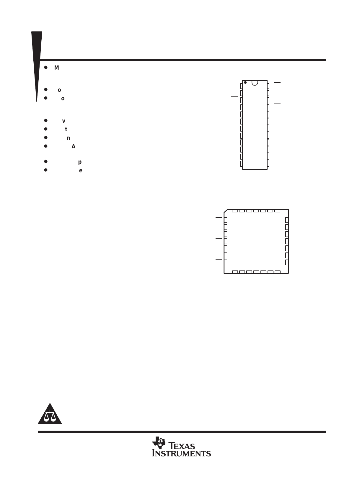
426
14 15 16 1718
4A
4Z
4LB
NC
V
GND
4B
1Z1AVNCNCVNC
FN PACKAGE
(TOP VIEW)
NC – No internal connection
CC2
CC1
EE
1
2
3
4
5
6
7
8
9
10
11
12
24
23
22
21
20
19
18
17
16
15
14
13
3A
3Z
3LB
4A
4Z
4LB
V
EE
GND
4B
4Y
3B
3Y
2LB
2Z
2A
1LB
1Z
1A
V
CC2
V
CC1
1Y
1B
2Y
2B
DW PACKAGE
(TOP VIEW)
Page 2
SN75186
QUADRUPLE DRIVER/RECEIVER WITH LOOPBACK
SLLS068C – FEBRUARY 1990 – REVISED MAY 1995
2
POST OFFICE BOX 655303 • DALLAS, TEXAS 75265
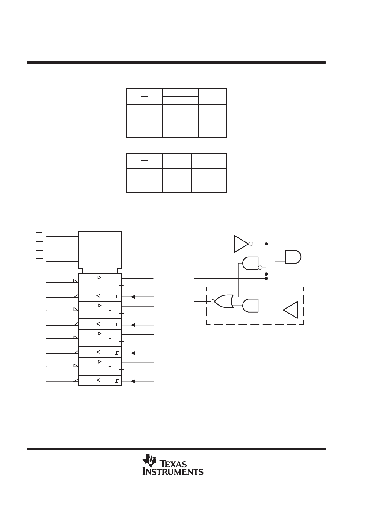
Function Tables
EACH RECEIVER
LOOPBACK
INPUTS
INPUT
LB
A B
†
DE
H X H L
H X LH
L LXL
L HXH
EACH DRIVER
LOOPBACK
INPUT OUTPUT
LB A Y
†
H H L
H L H
L X L
†
Voltages are EIA/TIA-232-E, and V .28 levels
H = high level, L = low level, X = irrelevant
logic symbol
‡
G1
21
G2
24
G3
3
G4
6
1Y
16
1
1V5
19
1A
20
1Z
1B
15
1
2Y
14
2
2V6
22
2A
6
23
2Z
2B
13
2
3Y
12
3
3V7
1
3A
4Y
10
4
4V8
4
4A
8
5
4Z
4B
9
4
7
2
3Z
3B
11
3
1LB
2LB
3LB
4LB
‡
This symbol is in accordance with ANSI/IEEE Std 91-1984 and
IEC Publication 617-12.
Pin numbers shown are for the DW package.
logic diagram, each driver/receiver pair
(positive logic)
Z
LB
A
Receiver
B
Y
Driver
Page 3
SN75186
QUADRUPLE DRIVER/RECEIVER WITH LOOPBACK
SLLS068C – FEBRUARY 1990 – REVISED MAY 1995
3
POST OFFICE BOX 655303 • DALLAS, TEXAS 75265
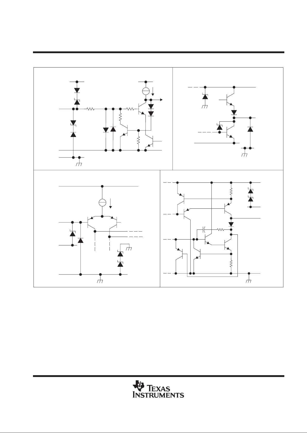
schematics of inputs and outputs
GND
8 V
8 V
GND
8 V
Internal
1.4-V Ref to GND
EQUIVALENT DRIVER AND LOOPBACK INPUT EQUIVALENT DRIVER OUTPUT
D1
Output
GND
V
CC1
3 pF
8 V
8 V
EQUIVALENT RECEIVER OUTPUT
8 V
8 V
GND
EQUIVALENT RECEIVER INPUT
GND
45 V
45 V
B Input
ESD Protection
GND
V
CC2
V
EE
Z Output
100 kΩ
1.2 x V
BE
ESD Protection
ESD Protection
V
CC1
V
CC2
2 kΩ
2 kΩ
4 kΩ
V
EE
V
CC1
ESD Protection
A Input
V
EE
ESD Protection
ESD
Protection
30 Ω
5 kΩ
30 Ω
V
EE
All component values shown are nominal.
Page 4
SN75186
QUADRUPLE DRIVER/RECEIVER WITH LOOPBACK
SLLS068C – FEBRUARY 1990 – REVISED MAY 1995
4
POST OFFICE BOX 655303 • DALLAS, TEXAS 75265
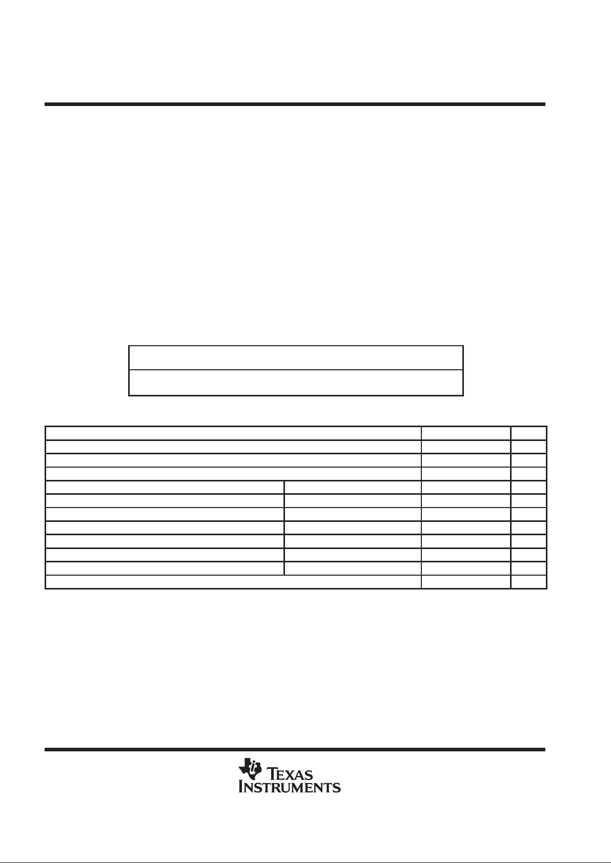
absolute maximum ratings over operating free-air temperature range (unless otherwise noted)
†
Supply voltage, V
CC1
(see Note 1) 15 V. . . . . . . . . . . . . . . . . . . . . . . . . . . . . . . . . . . . . . . . . . . . . . . . . . . . . . . . . . .
Supply voltage, V
CC2
7 V. . . . . . . . . . . . . . . . . . . . . . . . . . . . . . . . . . . . . . . . . . . . . . . . . . . . . . . . . . . . . . . . . . . . . . .
Supply voltage, V
EE
–15 V. . . . . . . . . . . . . . . . . . . . . . . . . . . . . . . . . . . . . . . . . . . . . . . . . . . . . . . . . . . . . . . . . . . . . . .
Receiver input voltage range, V
I
–30 V to 30 V. . . . . . . . . . . . . . . . . . . . . . . . . . . . . . . . . . . . . . . . . . . . . . . . . . . . .
Driver input voltage range, V
I
(VEE + 2 V) to V
CC1
. . . . . . . . . . . . . . . . . . . . . . . . . . . . . . . . . . . . . . . . . . . . . . . . . .
Loopback input voltage range, V
I
0 V to 7 V. . . . . . . . . . . . . . . . . . . . . . . . . . . . . . . . . . . . . . . . . . . . . . . . . . . . . . .
Driver output voltage range, V
O
–30 V to 30 V. . . . . . . . . . . . . . . . . . . . . . . . . . . . . . . . . . . . . . . . . . . . . . . . . . . . . .
Continuous total power dissipation See Dissipation Rating Table. . . . . . . . . . . . . . . . . . . . . . . . . . . . . . . . . . . . .
Operating free-air temperature range, T
A
0°C to 70°C. . . . . . . . . . . . . . . . . . . . . . . . . . . . . . . . . . . . . . . . . . . . . .
Storage temperature range, T
stg
–65°C to 150°C. . . . . . . . . . . . . . . . . . . . . . . . . . . . . . . . . . . . . . . . . . . . . . . . . . .
Case temperature for 10 seconds: FN package 260°C. . . . . . . . . . . . . . . . . . . . . . . . . . . . . . . . . . . . . . . . . . . . . .
Lead temperature 1,6 mm (1/16 inch) from case for 10 seconds: DW package 260°C. . . . . . . . . . . . . . . . . . .
†
Stresses beyond those listed under “absolute maximum ratings” may cause permanent damage to the device. These are stress ratings only, and
functional operation of the device at these or any other conditions beyond those indicated under “recommended operating conditions” is not
implied. Exposure to absolute-maximum-rated conditions for extended periods may affect device reliability.
NOTE 1: All voltages are with respect to the network ground terminal.
DISSIPATION RATING TABLE
PACKAGE
TA ≤ 25°C
POWER RATING
DERATING FACTOR
ABOVE TA = 25°C
TA = 70°C
POWER RATING
DW 1350 mW 10.8 mW/°C 864 mW
FN 1400 mW 11.2 mW/°C 896 mW
recommended operating conditions
MIN NOM MAX UNIT
Supply voltage, V
CC1
10.8 12 13.2 V
Supply voltage, V
CC2
4.5 5 5.5 V
Supply voltage, V
EE
–10.8 –12 –13.2 V
Input voltage, V
I
Driver and loopback 0 V
CC2
V
Input voltage, VI (see Note 2) Receiver ±30 V
High-level input voltage, V
IH
Driver and loopback 2 V
Low-level input voltage, V
IL
Driver and loopback 0.8 V
Output voltage powered on or off, V
O
Driver ±30 V
High-level output current, I
OH
Receiver –4 mA
Low-level output current, I
OL
Receiver 4 mA
Operating free-air temperature, T
A
0 70 °C
NOTE 2: If all receiver inputs are held at ±30 V , the thermal dissipation limit of the package may be exceeded. The thermal shutdown may not
protect the device, as this dissipation occurs in the receiver input resistors.
Page 5

SN75186
QUADRUPLE DRIVER/RECEIVER WITH LOOPBACK
SLLS068C – FEBRUARY 1990 – REVISED MAY 1995
5
POST OFFICE BOX 655303 • DALLAS, TEXAS 75265
DRIVER SECTION
electrical characteristics over full recommended ranges of supply voltage and operating free-air
temperature (unless otherwise noted)
PARAMETER TEST CONDITIONS MIN TYP†MAX UNIT
V
OH
High-level output voltage RL = 3 kΩ, VIL = 0.8 V, See Figure 1 7 V
V
OL
Low-level output voltage
‡
RL = 3 kΩ, VIH = 2 V, See Figure 1 –7 V
V
OH(LB)
High-level output voltage in
loopback mode
द
RL = 3 kΩ, LB at 0.8 V, VIL = 0.8 V –7 V
I
IH
High-level input current
(driver and loopback inputs)
#
VI = 5 V, See Figure 2 100 µA
I
IL
Low-level input current
(driver and loopback inputs)
#
–100 µA
V
OS(H)
High-level short-circuit output
current
VI = 0.8 V, VO = 0, See Note 3 and Figure 1 –10 –20 –35 mA
V
OS(L)
Low-level short-circuit output
current
VI = 2 V, VO = 0, See Note 3 and Figure 1 10 20 35 mA
I
CC1
Supply current from V
CC1
No load 2.5 4 mA
I
CC1(LB)
Supply current from V
CC1
with
loopback on
No load, LB at 0.8 V 10 mA
I
EE
Supply current from V
EE
No load –2.5 –4 mA
I
EE(LB)
Supply current from VEE with
loopback on
No load, LB at 0.8 V –10 mA
I
CC2
Supply current from V
CC2
No load, VI = 0, See Note 5 –10 –100 µA
I
CC2(LB)
Supply current from V
CC2
with
loopback on
No load,
See Note 5
LB at 0.8 V, VI = 0,
–10 –100 µA
r
o
Output resistance
V
CC1
= VEE = V
CC2
= 0,
See Note 4
VO = –2 V to 2 V,
0.3 5 kΩ
†
All typical values are at TA = 25°C.
‡
The algebraic convention, where the more positive (less negative) limit is designated as maximum, is used in this data sheet for logic levels only.
§
This is the most positive level to which the driver output rises when the device is in the loopback mode and the driver input is at a low level.
¶
The loopback mode should be entered only when the driver output is in the low (marking) state.
#
Unused driver inputs should be tied to 0 V or V
CC2;
unused loopback inputs should be tied to V
CC2.
NOTES: 3. Minimum I
OS(H)
and I
OS(L)
are specified at VO = 0, as this more accurately describes the output current needed to dynamically drive
capacitive lines. A minimum of ±10 mA is sufficient to drive 2500 pF in parallel with 3 kΩ at a slew rate of 4 V/µs ( in accordance
with EIA/TIA-232-E and V.28).
4. Test conditions are those specified by EIA/TIA-232-E.
5. Without a load and VI = 0, the worst-case conditions, V
CC2
sources a small current originating from V
CC1
giving I
CC2
supply current
a negative sign. When a receiver has an output load, V
CC2
sinks static and dynamic supply currents to meet load requirements.
Page 6

SN75186
QUADRUPLE DRIVER/RECEIVER WITH LOOPBACK
SLLS068C – FEBRUARY 1990 – REVISED MAY 1995
6
POST OFFICE BOX 655303 • DALLAS, TEXAS 75265
switching characteristics over full recommended ranges of supply voltages and operating free-air
temperature (unless otherwise noted)
PARAMETER TEST CONDITIONS MIN TYP†MAX UNIT
t
PLH
Propagation delay time, low- to high-level
output
R
= 3 kΩ to 7 kΩ, C
= 15 pF,
0.6 5 µs
t
PHL
Propagation delay time, high- to low-level
output
L
,
See Figure 3
L
,
0.8 5 µs
t
sk
| t
PLH
– t
PHL
| RL = 3 kΩ to 7 kΩ,CL = 15 pF to 2500 pF 0.2 1 µs
SR Output slew rate RL = 3 kΩ to 7 kΩ,CL = 15 pF to 2500 pF 4 30 V/µs
t
pd(ILB)
Propagation delay time going into loopback
mode
‡
RL = 3 kΩ to 7 kΩ, See Note 6 and Figure 7 3 50 µs
t
pd(OLB)
Propagation delay time going out of
loopback mode
§
RL = 3 kΩ to 7 kΩ, See Note 6 and Figure 7 3 50 µs
t
pd(LB)
Propagation delay time in loopback mode¶RL = 3 kΩ to 7 kΩ, See Note 6 and Figure 8 3 15 µs
t
sk
Skew time in loopback mode RL = 3 kΩ to 7 kΩ, See Note 6 4 10 µs
†
All typical values are at TA = 25°C.
‡
This is the delay between entering the loopback mode and when the data on the receiver output becomes valid.
§
This is the worst-case (rising or falling edges) total propagation delay between driver input and receiver output when in the loopback mode.
¶
This is the magnitude of the difference between the propagation delay time of the rising and falling edges of t
pd(LB)
.
NOTE 6: Skew time is the magnitude of the difference between t
PHL
and t
PLH
and is measured with a 0-to-3-V input pulse.
Page 7

SN75186
QUADRUPLE DRIVER/RECEIVER WITH LOOPBACK
SLLS068C – FEBRUARY 1990 – REVISED MAY 1995
7
POST OFFICE BOX 655303 • DALLAS, TEXAS 75265
RECEIVER SECTION
electrical characteristics over full recommended ranges of supply voltages and operating free-air
temperature (unless otherwise noted)
PARAMETER TEST CONDITIONS MIN TYP†MAX UNIT
V
IT+
Positive-going input threshold voltage See Figure 5 1.3 2 2.5 V
V
IT–
Negative-going input threshold voltage See Figure 5 0.5 1 1.7 V
V
hys
Input hysteresis voltage (V
IT+
– V
IT–
) 0.5 1 1.5 V
p
VI = –3 V or inputs open, IOH = –20 µA 3.5
VOHHigh-level output voltage
IOH = –4 mA, See Note 7 and Figure 5 2.4
V
p
I
= 4 mA, V
= 3 V,
VOLLow-level output voltage
OL
,
See Figure 5
I
,
0.4
V
I
OS(H)
Short-circuit output current at high level VOH = 0, See Figure 4 –20 –60 mA
I
OS(L)
Short-circuit output current at low level VOL = V
CC2
, See Figure 4 20 60 mA
p
VI ≤ 25 V 3
riInput resistance
VI = 3 V to 25 V 7
kΩ
†
All typical values are at TA = 25°C.
NOTE 7: If the inputs are left unconnected, the receiver interprets this as a low input and the receiver outputs will remain in the high state.
switching characteristics over full recommended ranges of supply voltages and operating free-air
temperature (unless otherwise noted)
PARAMETER TEST CONDITIONS MIN TYP†MAX UNIT
t
PLH
Propagation delay time, low- to high-level output
2 6 µs
t
PHL
Propagation delay time, high- to low-level output
See Figure 6
2 6 µs
t
TLH
Transition time, low- to high-level output
‡
p
200 300 ns
t
THL
Transition time, high- to low-level output
‡
C
L
= 50 pF,
See Figure 6
50 300 ns
t
sk
t
PLH
– t
PHL
0.1 1 µs
t
w
Maximum pulse duration assumed to be noise
§
Pulse amplitude = 5 V 1 2 4 µs
†
All typical values are at TA = 25°C.
‡
Transition times are measured between 10% and 90% points on output waveform.
§
The receiver will ignore any positive- or negative-going pulse whose duration is less than the minimum value of tw and accept any positive- or
negative-going pulse whose duration is greater than the maximum value of tw.
Page 8

SN75186
QUADRUPLE DRIVER/RECEIVER WITH LOOPBACK
SLLS068C – FEBRUARY 1990 – REVISED MAY 1995
8
POST OFFICE BOX 655303 • DALLAS, TEXAS 75265
PARAMETER MEASUREMENT INFORMATION
A
Y
V
CC1VCC2
V
I
V
EE
V
O
VEE or GND
V
CC1
or GND
–I
OS(H)
I
OS(L)
RL = 3 kΩ
Figure 1. Driver Test Circuit, VOH, VOL, I
OS(L)
, I
OS(H)
A
Y
V
CC1VCC2
V
EE
V
I
V
I
I
IH
–I
IL
Figure 2. Driver and Loopback Test Circuit, IIL, I
IH
(see Note C)
DRIVER VOLTAGE WAVEFORMS
DRIVER TEST CIRCUIT
Pulse
Generator
(see Note A)
0 V
3 V
Output Y
Input A
–3 V–3 V
50%50%
3 V 3 V
t
r
t
f
t
PLH
t
PHL
1.5 V1.5 V
C
L
(see Note B)
Input
A
Y
V
CC1VCC2
V
EE
R
L
V
OH
NOTES: A. The pulse generator has the following characteristics: tw = 25 µs, PRR = 20 kHz, ZO = 50 Ω.
B. CL includes probe and jig capacitance.
C. Slew rate =
6 V
tr or t
f
Figure 3. Driver Test Circuit and Voltage Waveforms
Page 9

SN75186
QUADRUPLE DRIVER/RECEIVER WITH LOOPBACK
SLLS068C – FEBRUARY 1990 – REVISED MAY 1995
9
POST OFFICE BOX 655303 • DALLAS, TEXAS 75265
PARAMETER MEASUREMENT INFORMATION
B
Z
V
CC1VCC2
V
EE
V
I
–I
OS(H)
I
OS(L)
V
CC2
Figure 4. Receiver Test Circuit, I
OS(H)
, I
OS(L)
B
Z
V
CC1VCC2
V
EE
V
OL
V
OH
–I
OH
I
OL
VIT, V
I
Figure 5. Receiver Test Circuit, VIT, VOL, V
OH
VOLTAGE WAVEFORMS
TEST CIRCUIT
(see Note B)
L
C
Input
B
Z
V
CC1VCC2
V
EE
–5 V
5 V
Output Z
Input B
10%10%
90% 90%
t
TLH
t
THL
t
PLH
t
PHL
V
OH
V
OL
Pulse
Generator
(see Note A)
50%
50%
50%
50%
NOTES: A. The pulse generator has the following characteristics: tw = 25 µs, PRR = 20 kHz, ZO = 50 Ω.
B. CL includes probe and jig capacitance.
Figure 6. Receiver Propagation and Transition Times
Page 10

SN75186
QUADRUPLE DRIVER/RECEIVER WITH LOOPBACK
SLLS068C – FEBRUARY 1990 – REVISED MAY 1995
10
POST OFFICE BOX 655303 • DALLAS, TEXAS 75265
PARAMETER MEASUREMENT INFORMATION
VOLTAGE WAVEFORMS
Output Z
Receiver
Input LB
Loopback
TEST CIRCUIT
B = High
A
Input
Y
LB
t
pd(ILB)
t
pd(OLB)
Pulse
Generator
(see Note A)
50%
50%
50%
50%
NOTES: A. The pulse generator has the following characteristics: tw = 25 µs, PRR = 20 kHz, ZO = 50 Ω.
B. CL includes probe and jig capacitance.
Figure 7. Loopback Entry and Exit Propagation Times
Driver
Input A
Driver
Receiver
B
VOLTAGE WAVEFORMS
Output Z
Receiver
TEST CIRCUIT
Input
Y
t
pd(LB)
t
pd(LB)
LB
= Low
Z
A
Pulse
Generator
(see Note A)
50%
50%
50%
50%
NOTES: A. The pulse generator has the following characteristics: tw = 25 µs, PRR = 20 kHz, ZO = 50 Ω.
B. CL includes probe and jig capacitance.
Figure 8. Loop Propagation Times in Loopback Mode
Page 11

SN75186
QUADRUPLE DRIVER/RECEIVER WITH LOOPBACK
SLLS068C – FEBRUARY 1990 – REVISED MAY 1995
11
POST OFFICE BOX 655303 • DALLAS, TEXAS 75265
PRINCIPLES OF OPERATION
In normal operation, the SN75186 acts as four independent drivers and receivers; the loopback mode is held off by
keeping logic inputs LB
high. Taking a particular LB input low activates the loopback mode in the corresponding
driver/receiver pair. This causes the output from that driver to be fed back to the input of its receiver through dedicated
internal loopback circuitry. Data from the receiver output can then be compared, by a communication system, with
the data transmitted to the driver to determine if the functional operation of the driver and receiver together is correct.
In the loopback mode, external data at the input of the receiver is ignored and the driver does not transmit data onto
the line. Extraneous data is prevented internally from being sent by the driver in the loopback mode by clamping its
output to a level below the maximum interface voltage, –5 V , or the EIA/TIA-232-E marking state. Below this marking
level, a reduced 1.5-V output amplitude is used at the driver output. This signal is detected by an on-chip loopback
comparator and fed to the input stage of the receiver to complete the loop.
Line faults external to the SN75186 are detected in addition to device failures. These line faults include short circuits
to ground and to external supply voltages that are greater than (V
EE
+ 7 V) and less than VEE typically . For example,
with V
EE
= –12 V , line short circuits to voltages greater than –5 V and less than –12 V will be detected. The loopback
mode should be entered only when the driver output is low, that is, the marking state of EIA/TIA-232-E. Loopback
should not be entered when the driver output is in a high state as this may cause a low-level, nondamaging oscillation
at the driver output.
When in the loopback mode, approximately 95% of the SN75186 circuit is functionally checked. There exists some
low probability of fault mechanisms in circuitry not being checked in the loopback mode. To reduce the chances of
undetected failure, the unchecked circuitry has been designed to be more robust than that within the loopback test
loop. The areas where special attention has been paid are the receiver input potential divider and resistors, the driver
output blocking diode (D1), and parts of the driver clamp circuit.
Protection of the SN75186 is achieved by means of driver output current limits and a thermal trip. Although this device
can withstand ±30 V at its receiver input, package thermal dissipation limitations have to be taken into consideration
if more than one receiver is connected simultaneously . This is due to the possible dissipation in the 3-kΩ minimum
input resistors, which is not under the control of the thermal trip. Although the supply current is higher in the loopback
mode than in normal operation, the total power dissipation is not sufficient under normal worst-case conditions (of
receiver input V
I
= 15 V + 10%, receiver output voltage = 2.4 V at 4 mA, driver load of 3 kΩ) to cause the thermal limiting
circuitry to trip.
If the SN75186 goes into thermal trip, the output of the driver goes to a high-impedance state and the receiver output
is held in a logic-high marking state. Both driver and receiver outputs maintain a marking state and do not allow
indeterminate conditions to exist.
The standards specify a minimum driver output resistance to ground of 300 Ω when the device is powered off. T o fully
comply with EIA/TIA-232-E power-off fault conditions, many drivers need diodes in series with each supply voltage
to prevent reverse current flow and driver damage. The SN75186 overcomes this need by providing a
high-impedance driver output of typically 5 kΩ under power-off conditions through the use of the equivalent of these
series diodes in the driver output circuit.
Page 12

IMPORTANT NOTICE
T exas Instruments and its subsidiaries (TI) reserve the right to make changes to their products or to discontinue
any product or service without notice, and advise customers to obtain the latest version of relevant information
to verify, before placing orders, that information being relied on is current and complete. All products are sold
subject to the terms and conditions of sale supplied at the time of order acknowledgement, including those
pertaining to warranty, patent infringement, and limitation of liability.
TI warrants performance of its semiconductor products to the specifications applicable at the time of sale in
accordance with TI’s standard warranty. Testing and other quality control techniques are utilized to the extent
TI deems necessary to support this warranty. Specific testing of all parameters of each device is not necessarily
performed, except those mandated by government requirements.
CERT AIN APPLICATIONS USING SEMICONDUCTOR PRODUCTS MAY INVOLVE POTENTIAL RISKS OF
DEATH, PERSONAL INJURY, OR SEVERE PROPERTY OR ENVIRONMENTAL DAMAGE (“CRITICAL
APPLICATIONS”). TI SEMICONDUCTOR PRODUCTS ARE NOT DESIGNED, AUTHORIZED, OR
WARRANTED TO BE SUITABLE FOR USE IN LIFE-SUPPORT DEVICES OR SYSTEMS OR OTHER
CRITICAL APPLICATIONS. INCLUSION OF TI PRODUCTS IN SUCH APPLICA TIONS IS UNDERST OOD TO
BE FULLY AT THE CUSTOMER’S RISK.
In order to minimize risks associated with the customer’s applications, adequate design and operating
safeguards must be provided by the customer to minimize inherent or procedural hazards.
TI assumes no liability for applications assistance or customer product design. TI does not warrant or represent
that any license, either express or implied, is granted under any patent right, copyright, mask work right, or other
intellectual property right of TI covering or relating to any combination, machine, or process in which such
semiconductor products or services might be or are used. TI’s publication of information regarding any third
party’s products or services does not constitute TI’s approval, warranty or endorsement thereof.
Copyright 1998, Texas Instruments Incorporated
 Loading...