

Page 1
Order this document by SN75175/D
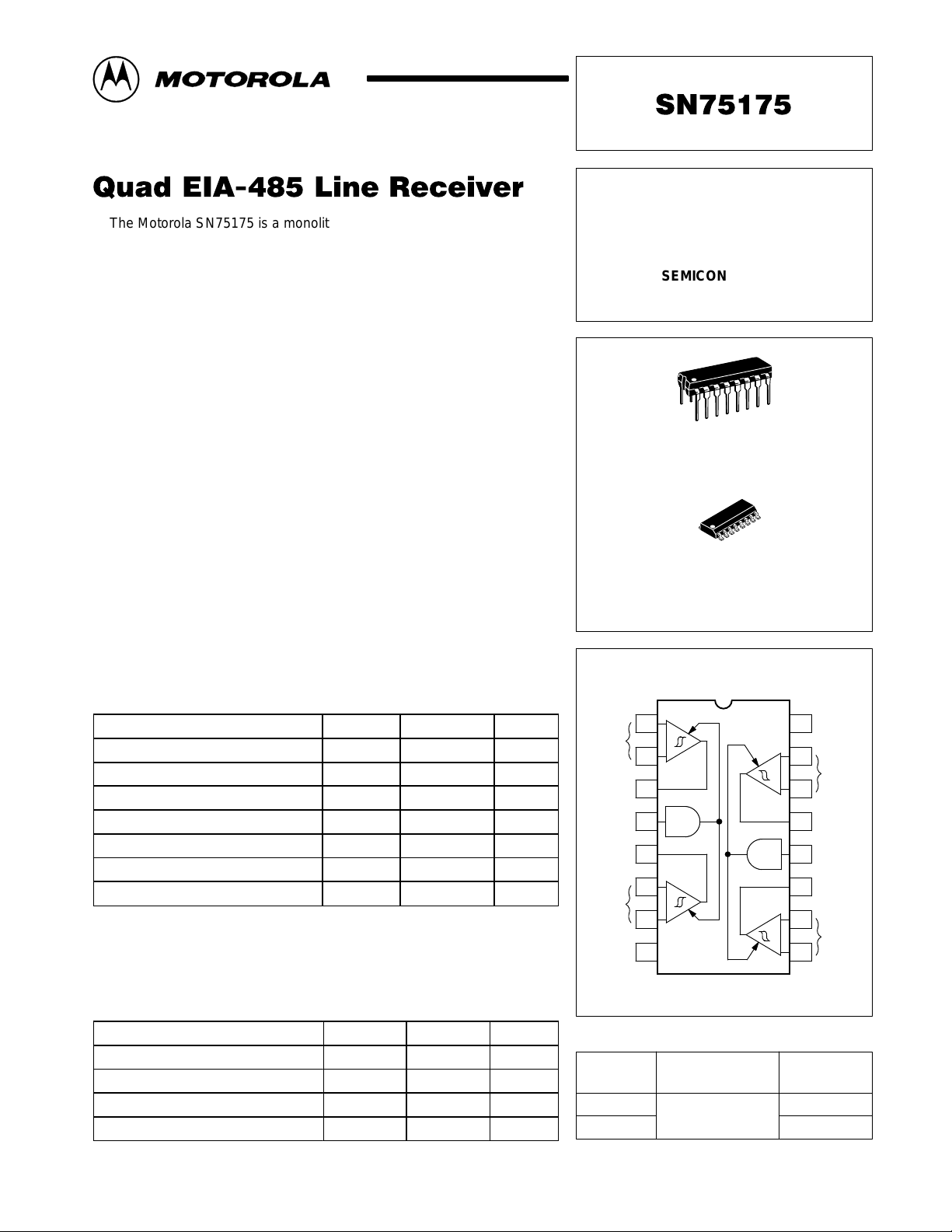
The Motorola SN75175 is a monolithic quad differential line receiver with
three–state outputs. It is designed specifically to meet the requirements of
EIA–485, EIA–422A/23A Standards and CCITT recommendations.
The device is optimized for balanced multipoint bus transmission at rates
up to 10 megabits per second. It also features high input impedance, input
hysteresis for increased noise immunity, and input sensitivity of ±200 mV
over a common mode input voltage range of –12 V to 12 V . The SN75175 is
designed for optimum performance when used with the SN75172 or
SN75174 quad differential line drivers.
• Meets EIA Standards EIA–422A and EIA–423A, EIA–485
• Meets CCITT Recommendations V.10, V.11, X.26, and X.27
• Designed for Multipoint Transmission on Long Bus Lines in Noisy
Environments
• 3–State Outputs
• Common–Mode Input Voltage Range . . . –12 V to 12 V
• Input Sensitivity . . . ±200 mV
• Input Hysteresis . . . 50 mV Typ
• High Input Impedance . . . 1 EIA–485 Unit Load
• Operates from Single 5.0 V Supply
• Lower Power Requirements
• Plug–In Replacement for MC3486
QUAD EIA–485
LINE RECEIVER WITH
THREE–STATE OUTPUTS
SEMICONDUCTOR
TECHNICAL DATA
16
1
N SUFFIX
PLASTIC PACKAGE
CASE 648
16
1
D SUFFIX
PLASTIC PACKAGE
CASE 751B
(SO–16)
This device contains 174 active transistors.
MAXIMUM RATINGS
Rating Symbol Value Unit
Power Supply Voltage V
Input Common Mode Voltage V
Input Differential Voltage V
Three–State Control Input Voltage V
Output Sink Current I
Storage Temperature T
Operating Junction Temperature T
NOTE: ESD data available upon request.
CC
ICM
ID
I
O
stg
J
RECOMMENDED OPERATING CONDITIONS
Rating Symbol Value Unit
Power Supply Voltage V
Operating Ambient Temperature T
Input Common Mode Voltage Range V
Input Differential Voltage Range V
CC
A
ICM
IDR
7.0 Vdc
±25 Vdc
±25 Vdc
7.0 Vdc
50 mA
–65 to +150 °C
+150 °C
4.75 to 5.25 Vdc
0 to +70 °C
–12 to +12 Vdc
–12 to +12 Vdc
Inputs
A
Output
A
3–State
Control
A/C
Output
C
Inputs
C
Gnd
Device
SN75175N
SN75175D
PIN CONNECTIONS
1
–
+
2
3
4
5
6
+
–
7
8
(Top View)
16
15
–
+
14
13
12
11
10
+
–
9
ORDERING INFORMATION
Operating
Temperature Range
TA = 0 to +70°C
Plastic DIP
V
CC
Inputs
B
Output
B
3–State
Control
B/D
Output
D
Inputs
D
Package
SO–16
MOTOROLA ANALOG IC DEVICE DATA
Motorola, Inc. 1996 Rev 0
1
Page 2
SN75175
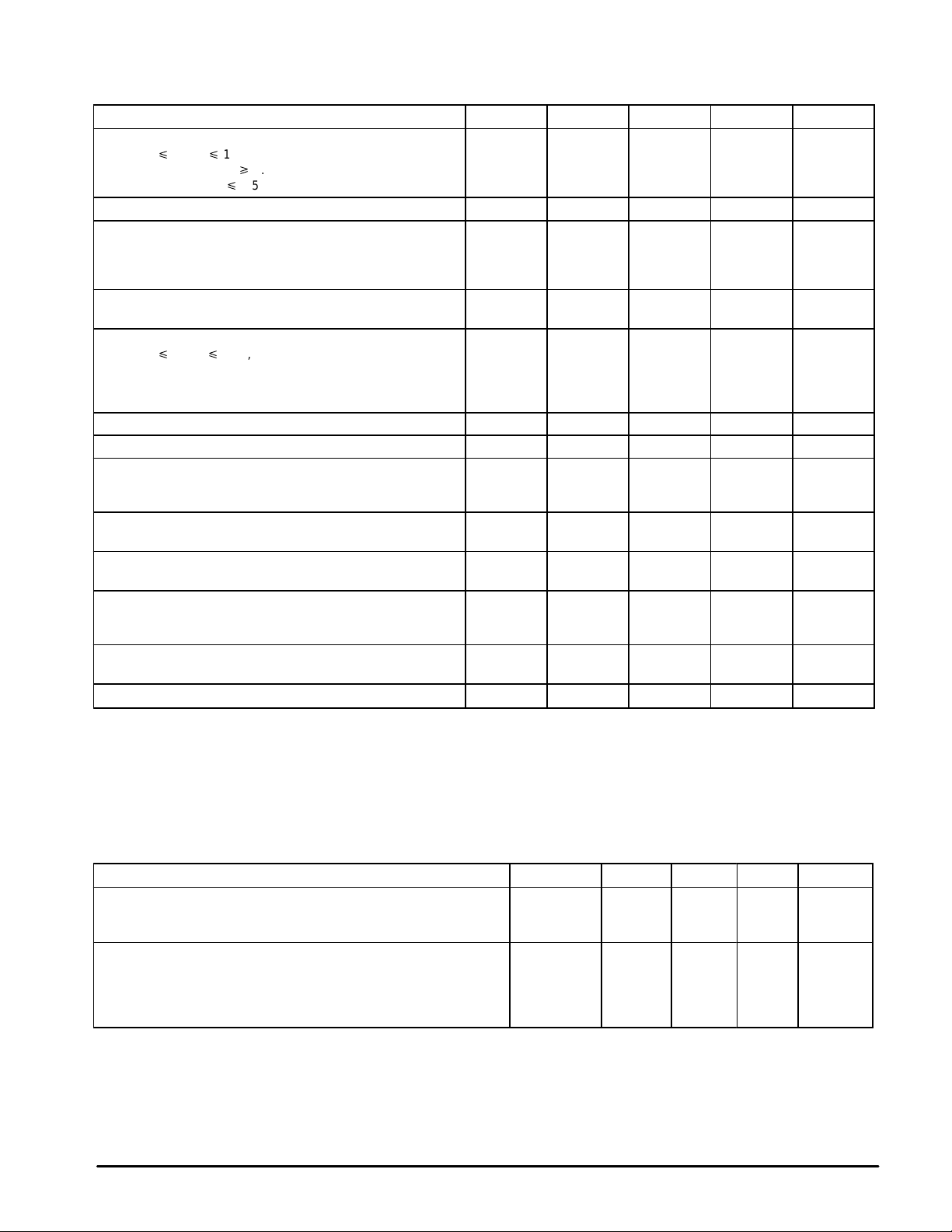
ELECTRICAL CHARACTERISTICS (Unless otherwise noted, minimum and maximum limits apply over recommended temperature and
power supply voltage ranges. Typical values are for TA = 25°C, VCC = 5.0 V, and V
Characteristic
Differential Input Threshold Voltage (Note 2)
(–12 V p V
(IO = –0.4 mA, VOH q 2.7 V)
(IO = 16 mA, VOL p 0.5 V)
Input Hysteresis VT+ – V
Input Line Current (Differential Inputs)
(Unmeasured Input at 0 V , Note 3)
(VI = 12 V)
(VI = –7.0 V)
Input Resistance (Note 4) r
Input Balance and Output Level (Note 3)
(–12 V pV
(IO = –0.4 mA, VID = 0.2 V)
(IO = 8.0 mA, VID = –0.2 V)
(IO = 16 mA, VID = –0.2 V)
Input Voltage – High Logic State (Three–State Control) V
Input Voltage – Low Logic State (Three–State Control) V
Input Current – High Logic State (Three–State Control)
(VIH = 2.7 V)
(VIH = 5.5 V)
Input Current – Low Logic State (Three–State Control)
(VIL = 0.4 V)
Input Clamp Diode Voltage (Three–State Control)
(IIK = –18 mA)
Output Third State Leakage Current
(V
= 3.0 V, VIL = 0.8 V, VO = 0.4 V)
I(D)
(V
= –3.0 V, VIL = 0.8 V, VO = 2.4 V)
I(D)
Output Short–Circuit Current (Note 5)
(V
= 3.0 V, VIH = 2.0 V, VO = 0 V)
I(D)
Power Supply Current (VIL = 0 V) (All Inputs Grounded) I
NOTES: 1. All currents into device pins are shown as positive, out of device pins are negative. All voltages referenced to ground unless otherwise noted.
2.Differential input threshold voltage and guaranteed output levels are done simultaneously for worst case.
3.Refer to EIA–485 for exact conditions. Input balance and guaranteed output levels are done simultaneously for worst case.
4.Input resistance should be derived from input line current specifications and is shown for reference only. See EIA–485 and input line current
specifications for more specific input resistance information.
5.Only one output at a time should be shorted.
p 12 V, VIH = 2.0 V)
ICM
p 12 V, VIH = 2.0 V)
ICM
Symbol Min Typ Max Unit
V
TH(D)
T–
I
I
i
V
OH
V
OL
V
OL
IH
IL
I
IH
I
IL
V
IK
I
OZ
I
OS
CC
= 0 V, Note 1.)
ICM
–
–
– 50 – mV
–
–
1 Unit
Load
2.7
–
–
2.0 – – V
– – 0.8 V
–
–
– – –100 µA
– – –1.5 V
–
–
–15 – –85 mA
– – 70 mA
–
–
–
–
– –
–
–
–
–
–
–
–
–0.2
–0.8
0.45
20
100
–20
0.2
1.0
–
0.5
20
V
mA
V
µA
µA
SWITCHING CHARACTERISTICS (Unless otherwise noted, V
Characteristic Symbol Min Typ Max Unit
Propagation Delay Time – Differential Inputs to Output
Output High to Low
Output Low to High
Propagation Delay Time – Three–State Control to Output
Output Low to Third State
Output High to Third State
Output Third State to High
Output Third State to Low
2
= 5.0 V and TA = 25°C.)
CC
t
PHL(D)
t
PLH(D)
t
PLZ
t
PHZ
t
PZH
t
PZL
–
–
–
–
–
–
25
25
16
19
11
11
35
35
35
35
30
30
ns
ns
MOTOROLA ANALOG IC DEVICE DATA
Page 3
SN75175
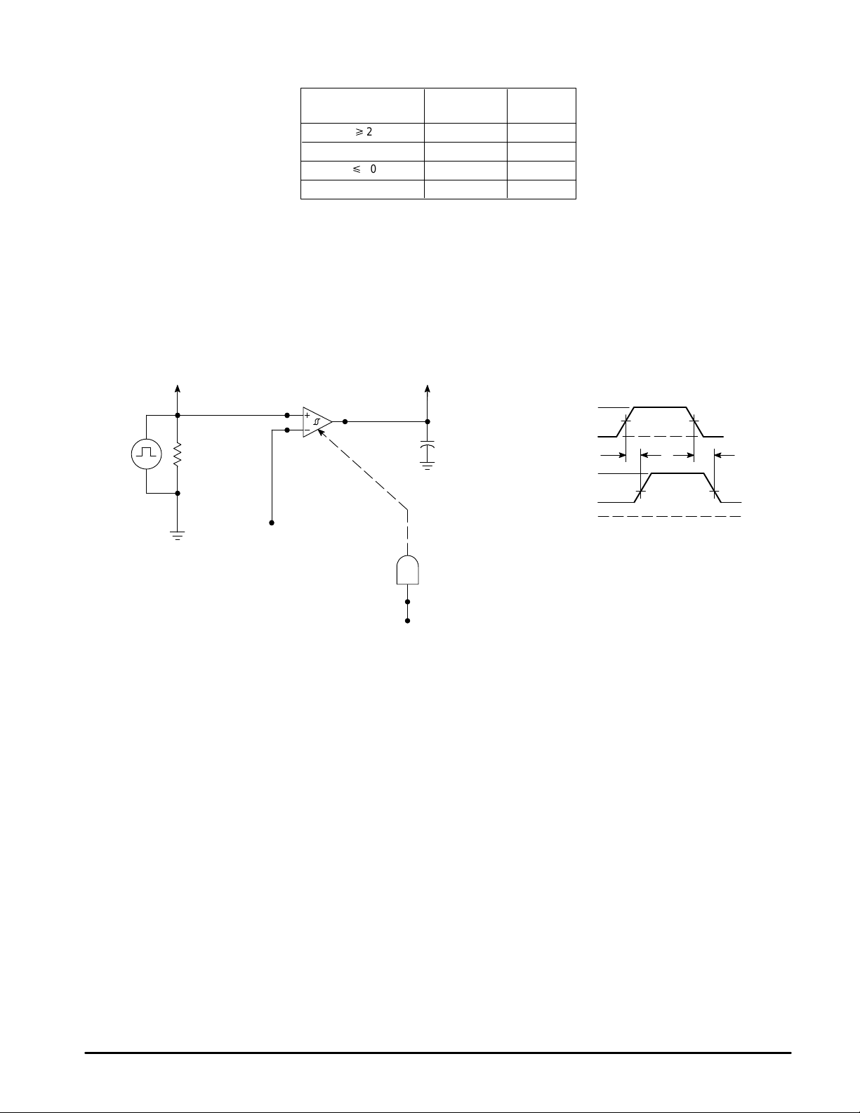
FUNCTION TABLE (EACH RECEIVER)
Differential Inputs Output
VIDq
2.0 V
–0.2 V<VID<0.2 V
VIDp
–0.2 V
XLZ
H = high level
L = low level
X = irrelevant
SWITCHING TEST CIRCUIT AND WAVEFORMS
Figure 1. Propagation Delay, Differential Input to Output
3–State
Control
HH
H?
HL
? = indeterminate
Z = high–impedance (off)
Y
Pulse
Generator
To Scope
(Input)
51
Differential
Inputs
1.5 V
2.0 V
3–State Control
To Scope
(Output)
(Includes Probe
Capacitance)
CL = 15 pF
and Stray
3.0 V
Input 1.5 V
0 V
t
PLH(D)
V
OH
V
OL
0 V
Input Pulse Characteristics –
t
= t
TLH
THL
PRR = 1.0 MHz, 50% Duty Cycle
1.5 V
Output
1.3 V
= 6.0 ns (10% to 90%)
t
PHL(D)
1.3 V
MOTOROLA ANALOG IC DEVICE DATA
3
Page 4

Figure 2. Propagation Delay, Three–State Control Input to Output
Input Pulse Characteristics –
t
= t
TLH
PRR = 1.0 MHz, 50% Duty Cycle
= 6.0 ns (10% to 90%)
THL
1.5 V for t
–1.5 V for t
Pulse
Generator
and t
PHZ
and t
PLZ
SN75175
SWITCHING TEST CIRCUIT AND WAVEFORMS (continued)
To Scope
(Input)
To Scope
(Output)
51
–
PZH
PZL
+
Differential
Inputs
CL = 15 pF
(Includes Probe
and Stray
Capacitance)
5.0 k
SW2
2.0 k
All Diodes 1N916
SW1
5.0 V
or Equivalent
Input
Output
Input
[
3.0 V
0 V
1.3 V
V
OL
3.0 V
0 V
V
OH
0 V
t
PLZ
1.5 V 1.5 V
t
PLZ
0.5 V
t
PZH
1.5 V
1.5 V
SW1 Closed
SW2 Closed
SW1 Open
SW2 Closed
t
PZH
1.5 V
0 V
E
Input
[
5.0 V – V
Output
E
out
in
[
3.0 V
0 V
V
OH
1.3 V
3.0 V
0 V
BE
V
OL
t
PHZ
1.5 V
0.5 V
t
PZL
1.5 V
t
PHZ
1.5 V
1.5 V
1.5 V
SW1 Closed
SW2 Closed
0 V
SW1 Closed
SW2 Open
t
PZL
0 V
4
MOTOROLA ANALOG IC DEVICE DATA
Page 5

SN75175
TYPICAL CHARACTERISTICS
5.0
4.0
3.0
2.0
O
V , OUTPUT VOL TAGE (V)
1.0
0
–140 –60–100
5.0
4.0
3.0
Figure 3. Output Voltage versus
Differential Input Voltage
VCC = 5.0 V
°
C
TA = 25
VCM = –12 V
VID, DIFFERENTIAL INPUT VOLTAGE (mV)
Figure 5. High Level Output Voltage
versus Output Current
VID = 0.2 V
TA = 25
VCC = 5.25 V
VCM = +12 V
100 14060200–20
°
C
Figure 4. Output Voltage versus
3–State Control Voltage
5.0
4.0
VCC = 5.0 V
3.0
2.0
O
V , OUTPUT VOL TAGE (V)
1.0
0
0.5
0 3.02.5
1.0 2.0 3.5 4.01.5
VI, 3–STATE CONTROL VOLTAGE (V)
Figure 6. Low Level Output Voltage
0.5
0.4
0.3
versus Output Current
VCC = 5.25 V
VCC = 4.75 V
VID = 0.2 V
Load = 8.0 k
°
C
TA = 25
Ω
to Gnd
V , HIGH LEVEL OUTPUT VOLTAGE (V)
V , HIGH LEVEL OUTPUT VOLTAGE (V)
OH
OH
2.0
VCC = 4.75 V
1.0
0
0
IOH, HIGH LEVEL OUTPUT CURRENT (mA)
VCC = 5.0 V
–10 –15
–
20 –25
Figure 7. High Level Output Voltage
5.0
4.5
4.0
3.5
3.0
2.5
2.0
1.5
1.0
0.5
0
10 10090
versus T emperature
20
30 40 00 403020
TA, FREE AIR TEMPERATURE (
50 60 70 80
VCC = 5.0 V
IOH = 400
µ
°
C)
A
–35
0.2
0.1
OL
V , LOW LEVEL OUTPUT VOLTAGE (V)
0
5.0
–40–30–5.0
035
IOL, LOW LEVEL OUTPUT CURRENT (mA)
15 2010
VCC = 5.0 V
°
C
TA = 25
25 40
30
Figure 8. Low Level Output Voltage
versus T emperature
0.5
0.4
0.3
VCC = 5.0 V
IOL = 16 mA
80706050 90 10010
°
C)
OL
V , LOW LEVEL OUTPUT VOLTAGE (V)
0.2
0.1
0
IA, FREE AIR TEMPERATURE (
MOTOROLA ANALOG IC DEVICE DATA
5
Page 6

SN75175
OUTLINE DIMENSIONS
–T–
–A–
916
PLASTIC PACKAGE
B
18
F
C
S
SEATING
–T–
PLANE
H
G
D
16 PL
0.25 (0.010) T
K
M
M
A
PLASTIC PACKAGE
–A–
16 9
–B–
18
8 PLP
0.25 (0.010) B
G
K
C
SEATING
PLANE
D
16 PL
0.25 (0.010) A
M
S
B
T
S
M
N SUFFIX
CASE 648–08
ISSUE R
L
J
D SUFFIX
CASE 751B–05
(SO–16)
ISSUE J
M
S
R
X 45
NOTES:
1. DIMENSIONING AND TOLERANCING PER ANSI
Y14.5M, 1982.
2. CONTROLLING DIMENSION: INCH.
3. DIMENSION L TO CENTER OF LEADS WHEN
FORMED PARALLEL.
4. DIMENSION B DOES NOT INCLUDE MOLD FLASH.
5. ROUNDED CORNERS OPTIONAL.
DIM MIN MAX MIN MAX
A 0.740 0.770 18.80 19.55
B 0.250 0.270 6.35 6.85
C 0.145 0.175 3.69 4.44
D 0.015 0.021 0.39 0.53
F 0.040 0.70 1.02 1.77
G 0.100 BSC 2.54 BSC
M
_
F
J
H 0.050 BSC 1.27 BSC
J 0.008 0.015 0.21 0.38
K 0.110 0.130 2.80 3.30
L 0.295 0.305 7.50 7.74
M 0 10 0 10
S 0.020 0.040 0.51 1.01
NOTES:
1. DIMENSIONING AND TOLERANCING PER ANSI
Y14.5M, 1982.
2. CONTROLLING DIMENSION: MILLIMETER.
3. DIMENSIONS A AND B DO NOT INCLUDE
MOLD PROTRUSION.
4. MAXIMUM MOLD PROTRUSION 0.15 (0.006)
PER SIDE.
5. DIMENSION D DOES NOT INCLUDE DAMBAR
PROTRUSION. ALLOWABLE DAMBAR
PROTRUSION SHALL BE 0.127 (0.005) TOTAL
IN EXCESS OF THE D DIMENSION AT
MAXIMUM MATERIAL CONDITION.
DIM MIN MAX MIN MAX
A 9.80 10.00 0.386 0.393
B 3.80 4.00 0.150 0.157
C 1.35 1.75 0.054 0.068
D 0.35 0.49 0.014 0.019
F 0.40 1.25 0.016 0.049
G 1.27 BSC 0.050 BSC
J 0.19 0.25 0.008 0.009
K 0.10 0.25 0.004 0.009
M 0 7 0 7
P 5.80 6.20 0.229 0.244
R 0.25 0.50 0.010 0.019
MILLIMETERSINCHES
____
INCHESMILLIMETERS
____
6
MOTOROLA ANALOG IC DEVICE DATA
Page 7

SN75175
Motorola reserves the right to make changes without further notice to any products herein. Motorola makes no warranty , representation or guarantee regarding
the suitability of its products for any particular purpose, nor does Motorola assume any liability arising out of the application or use of any product or circuit, and
specifically disclaims any and all liability, including without limitation consequential or incidental damages. “T ypical” parameters which may be provided in Motorola
data sheets and/or specifications can and do vary in different applications and actual performance may vary over time. All operating parameters, including “Typicals”
must be validated for each customer application by customer’s technical experts. Motorola does not convey any license under its patent rights nor the rights of
others. Motorola products are not designed, intended, or authorized for use as components in systems intended for surgical implant into the body, or other
applications intended to support or sustain life, or for any other application in which the failure of the Motorola product could create a situation where personal injury
or death may occur. Should Buyer purchase or use Motorola products for any such unintended or unauthorized application, Buyer shall indemnify and hold Motorola
and its officers, employees, subsidiaries, affiliates, and distributors harmless against all claims, costs, damages, and expenses, and reasonable attorney fees
arising out of, directly or indirectly, any claim of personal injury or death associated with such unintended or unauthorized use, even if such claim alleges that
Motorola was negligent regarding the design or manufacture of the part. Motorola and are registered trademarks of Motorola, Inc. Motorola, Inc. is an Equal
Opportunity/Affirmative Action Employer.
MOTOROLA ANALOG IC DEVICE DATA
7
Page 8

SN75175
How to reach us:
USA/EUROPE/Locations Not Listed: Motorola Literature Distribution; JAPAN: Nippon Motorola Ltd.; Tatsumi–SPD–JLDC, 6F Seibu–Butsuryu–Center,
P.O. Box 20912; Phoenix, Arizona 85036. 1–800–441–2447 or 602–303–5454 3–14–2 Tatsumi Koto–Ku, Tokyo 135, Japan. 03–81–3521–8315
MFAX: RMF AX0@email.sps.mot.com – TOUCHT ONE 602–244–6609 ASIA/PACIFIC: Motorola Semiconductors H.K. Ltd.; 8B Tai Ping Industrial Park,
INTERNET: http://Design–NET.com 51 Ting Kok Road, Tai Po, N.T., Hong Kong. 852–26629298
8
◊
MOTOROLA ANALOG IC DEVICE DATA
SN75175/D
*SN75175/D*
 Loading...