

Datasheet SN74TVC16222ADGGR, SN74TVC16222ADGVR, SN74TVC16222ADL, SN74TVC16222ADLR Datasheet (Texas Instruments)
Page 1
SN74TVC16222A
22-BIT VOLTAGE CLAMP
SCDS087B – APRIL 1999 – REVISED NOVEMBER 1999
D
Designed to Be Used in Voltage-Limiting
Applications
D
6.5-Ω On-State Connection Between Ports
A and B
D
Flow-Through Pinout for Ease of Printed
Circuit Board Trace Routing
D
Direct Interface With GTL+ Levels
D
ESD Protection Exceeds JESD 22
– 2000-V Human-Body Model (A114-A)
– 200-V Machine Model (A115-A)
– 1000-V Charged-Device Model (C101)
D
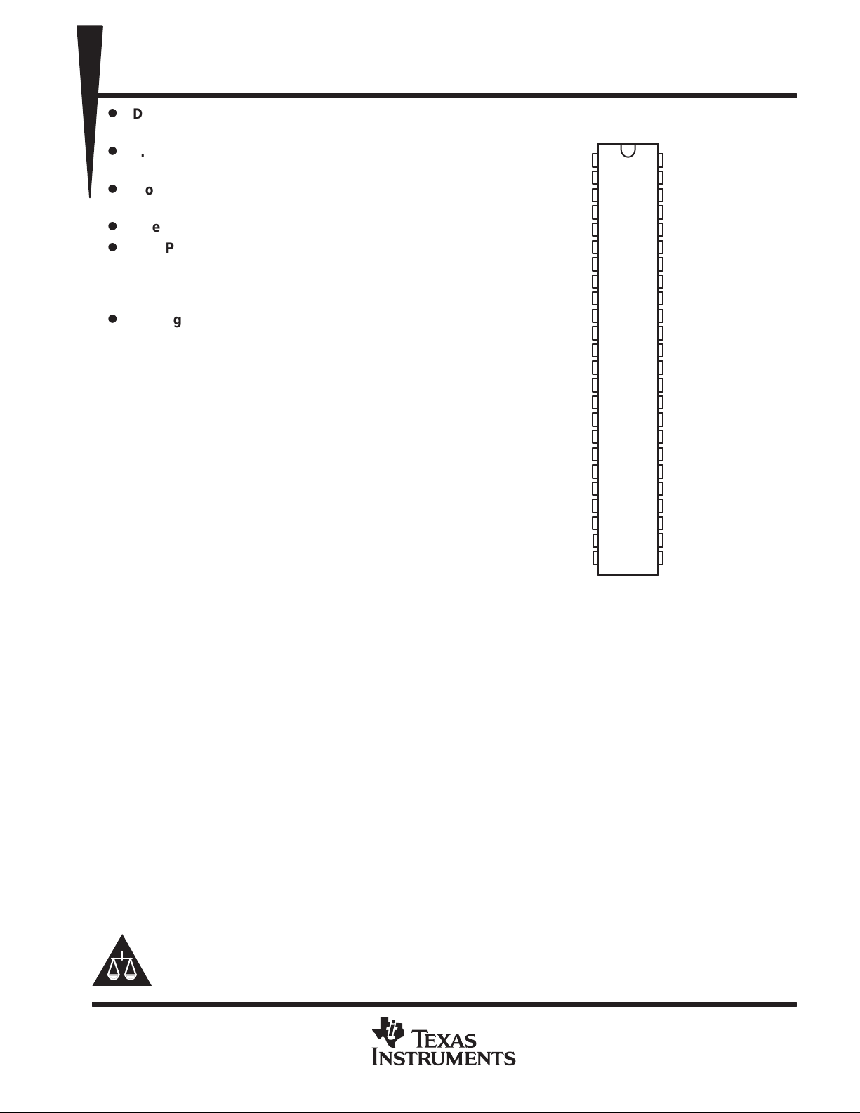
Package Options Include Plastic 300-mil
Shrink Small-Outline (DL), Thin Shrink
Small-Outline (DGG), and Thin Very
Small-Outline (DGV) Packages
description
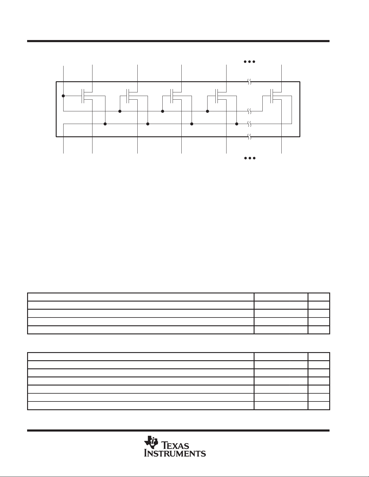
The SN74TVC16222A provides 23 parallel
NMOS pass transistors with a common gate. The
low on-state resistance of the switch allows
connections to be made with minimal propagation
delay .
The device can be used as a 22-bit switch with the
gates cascaded together to a reference transistor.
The low-voltage side of each pass transistor is
limited to a voltage set by the reference transistor.
This is done to protect components with inputs
that are sensitive to high-state voltage-level
overshoots. (See
data sheet.)
Application Information
in this
DGG, DGV, OR DL PACKAGE
GND
A1
A2
A3
A4
A5
A6
A7
A8
A9
A10
A11
A12
A13
A14
A15
A16
A17
A18
A19
A20
A21
A22
A23
(TOP VIEW)
1
48
2
47
3
46
4
45
5
44
6
43
7
42
8
41
9
40
10
39
11
38
12
37
13
36
14
35
15
34
16
33
17
32
18
31
19
30
20
29
21
28
22
27
23
26
24
25
GATE
B1
B2
B3
B4
B5
B6
B7
B8
B9
B10
B11
B12
B13
B14
B15
B16
B17
B18
B19
B20
B21
B22
B23
All of the transistors in the TVC array have the same electrical characteristics; therefore, any one of them can
be used as the reference transistor. Because, within the device, the characteristics from transistor-to-transistor
are equal, the maximum output high-state voltage (VOH) is approximately the reference voltage (V
minimum deviation from one output to another. This is a benefit of the TVC solution over discrete devices.
Because the fabrication of the transistors is symmetrical, either port connection of each bit can be used as the
low-voltage side, and the I/O signals are bidirectional through each FET.
The SN74TVC16222A is characterized for operation from –40°C to 85°C.
Please be aware that an important notice concerning availability, standard warranty, and use in critical applications of
Texas Instruments semiconductor products and disclaimers thereto appears at the end of this data sheet.
TI is a trademark of Texas Instruments Incorporated.
PRODUCTION DATA information is current as of publication date.
Products conform to specifications per the terms of Texas Instruments
standard warranty. Production processing does not necessarily include
testing of all parameters.
POST OFFICE BOX 655303 • DALLAS, TEXAS 75265
Copyright 1999, Texas Instruments Incorporated
REF
), with
1
Page 2
SN74TVC16222A
22-BIT VOLTAGE CLAMP
SCDS087B – APRIL 1999 – REVISED NOVEMBER 1999
simplified schematic
GATE B1 B2 B3 B4 B23
48 47 46 45 44 25
12 3 4 5 24
GND A1 A2 A3 A4 A23
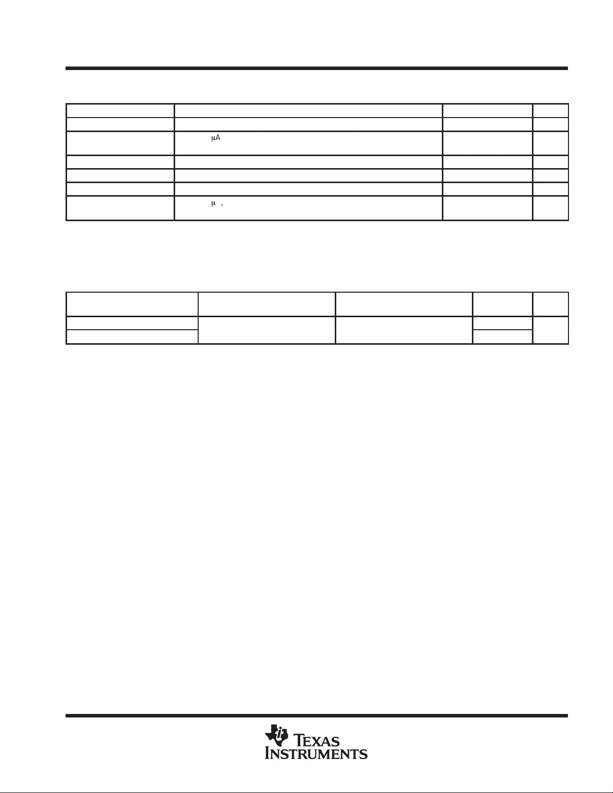
absolute maximum ratings over operating free-air temperature range (unless otherwise noted)
Input voltage range, V
Input/output voltage range, V
(see Note 1) –0.5 V to 7 V. . . . . . . . . . . . . . . . . . . . . . . . . . . . . . . . . . . . . . . . . . . . . . . . . .
I
(see Note 1) –0.5 V to 7 V. . . . . . . . . . . . . . . . . . . . . . . . . . . . . . . . . . . . . . . . . .
I/O
†
Continuous channel current 128 mA. . . . . . . . . . . . . . . . . . . . . . . . . . . . . . . . . . . . . . . . . . . . . . . . . . . . . . . . . . . . . .
Input clamp current, I
Package thermal impedance, θ
(V
< 0) –50 mA. . . . . . . . . . . . . . . . . . . . . . . . . . . . . . . . . . . . . . . . . . . . . . . . . . . . . . . . . . .
IK
I
(see Note 2): DGG package 70°C/W. . . . . . . . . . . . . . . . . . . . . . . . . . . . . . .
JA
DGV package 58°C/W. . . . . . . . . . . . . . . . . . . . . . . . . . . . . . . .
DL package 63°C/W. . . . . . . . . . . . . . . . . . . . . . . . . . . . . . . . .
Storage temperature range, T
†
Stresses beyond those listed under “absolute maximum ratings” may cause permanent damage to the device. These are stress ratings only, and
functional operation of the device at these or any other conditions beyond those indicated under “recommended operating conditions” is not
implied. Exposure to absolute-maximum-rated conditions for extended periods may affect device reliability.
NOTES: 1. The input and input/output negative-voltage ratings may be exceeded if the input and input/output clamp-current ratings are
observed.
2. The package thermal impedance is calculated in accordance with JESD 51.
–65°C to 150°C. . . . . . . . . . . . . . . . . . . . . . . . . . . . . . . . . . . . . . . . . . . . . . . . . . .
stg
recommended operating conditions
MIN TYP MAX UNIT
V
I/O
V
GATE
I
PASS
T
A
Input/output voltage 0 5 V
GATE voltage 0 5 V
Pass-transistor current 20 64 mA
Operating free-air temperature –40 85 °C
application operating conditions (see Figure 2)
MIN TYP MAX UNIT
V
BIAS
V
REF
V
DPU
I
PASS
I
REF
T
A
BIAS voltage 3 3.3 3.6 V
Reference voltage 1.365 1.5 1.635 V
Drain pullup voltage 2.36 2.5 2.64 V
Pass-transistor current 14 mA
Reference-transistor current 5 µA
Operating free-air temperature –40 85 °C
2
POST OFFICE BOX 655303 • DALLAS, TEXAS 75265
Page 3
A or B
B or A
ns
SN74TVC16222A
22-BIT VOLTAGE CLAMP
SCDS087B – APRIL 1999 – REVISED NOVEMBER 1999
electrical characteristics over recommended operating free-air temperature range (unless
otherwise noted)
PARAMETER TEST CONDITIONS MIN TYP†MAX UNIT
V
IK
V
OL
C
i(GATE)
C
io(OFF)
C
io(ON)
‡
r
on
†
All typical values are at TA = 25°C.
‡
Measured by the voltage drop between the A and B terminals at the indicated current through the switch. On-state resistance is determined by
the lower voltage of the two (A or B) terminals.
switching characteristics over recommended operating free-air temperature range,
V
= 2.36 V to 2.64 V (unless otherwise noted) (see Figure 1)
DPU
PARAMETER
t
PLH
t
PHL
V
= 0, II = –18 mA –1.2 V
BIAS
I
= 5 mA,
REF
V
= 2.625 V,
DPU
VI = 3 V or 0 73 pF
VO = 3 V or 0 4 12 pF
VO = 3 V or 0 12 25 pF
I
= 5 mA,
REF
V
= 2.625 V,
DPU
V
REF
R
DPU
V
REF
R
DPU
FROM
(INPUT)
= 1.365 V,
= 150 Ω,
= 1.365 V,
= 150 Ω,
VS = 0.175 V,
(see Figure 2)
VS = 0.175 V,
(see Figure 2)
TO
(OUTPUT)
350 mV
12.5 Ω
MIN MAX UNIT
0 4
0 4
POST OFFICE BOX 655303 • DALLAS, TEXAS 75265
3
Page 4
SN74TVC16222A
22-BIT VOLTAGE CLAMP
SCDS087B – APRIL 1999 – REVISED NOVEMBER 1999
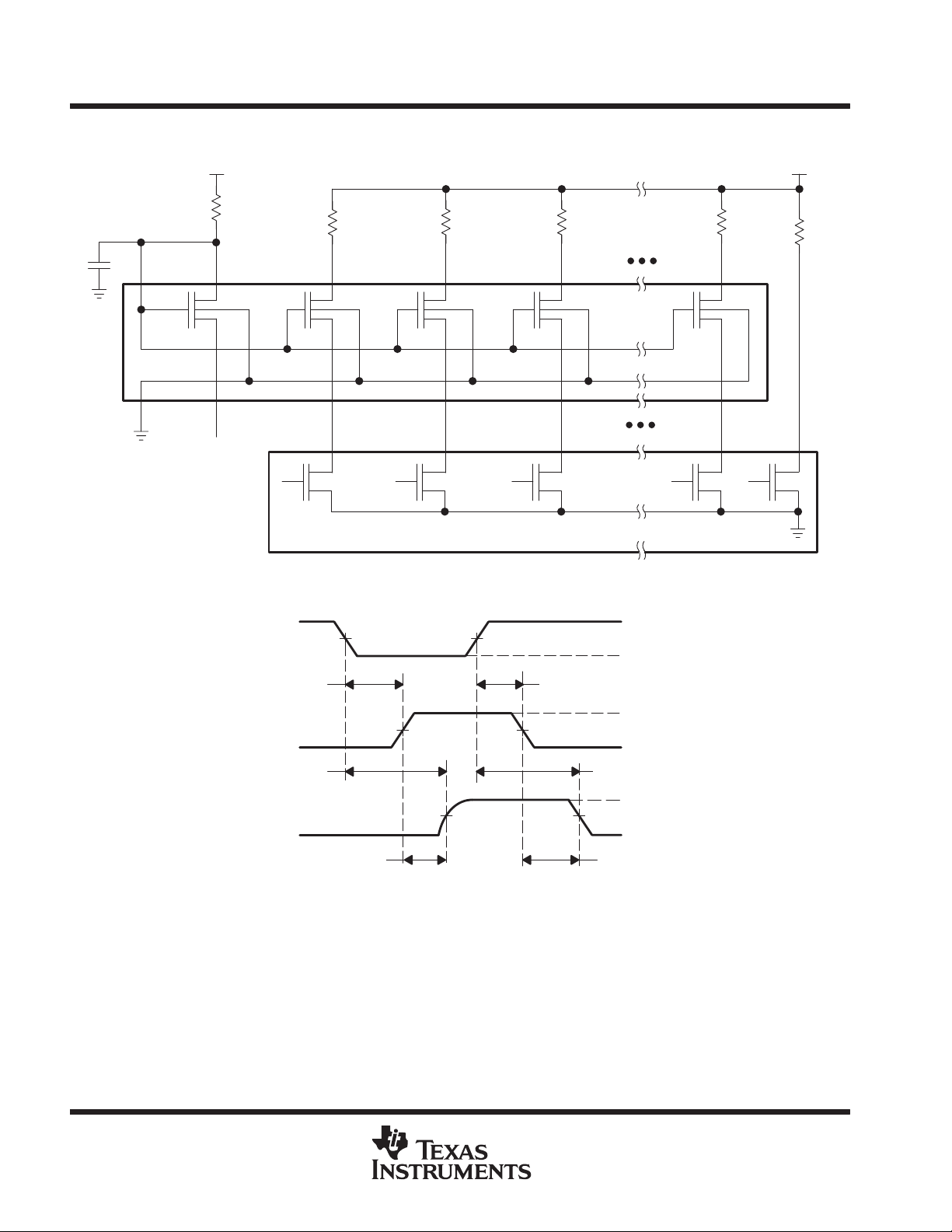
PARAMETER MEASUREMENT INFORMATION
Motherboard
Interface
GATE
48
TVC16222A
1
3.3 V
200 kΩ
B1 (V
47
2
A1 (V
Open-Drain
Test Interface
BIAS
REF
V
DPU
R
R
R
R
=
DPU
150 Ω
)
)
B2
46
3
A2 (VS)
TESTER CALIBRATION SETUP (see Note C)
DPU
150 Ω
B3
45
4
A3 (VS)
=
DPU
150 Ω
B4
44
5
A4 (VS)
=
DPU
150 Ω
B23
25
24
A23 (VS)
=
Input
GATE
Tester
t
PLHREF
Output
Reference
t
PLHDUT
Output
Device
Under Test
(see Note D)
NOTES: A. All input pulses are supplied by generators having the following characteristics: PRR ≤ 10 MHz, ZO = 50 Ω, tr ≤ 2 ns, tf ≤ 2 ns.
B. The outputs are measured one at a time with one transition per measurement.
C. Test procedure: t
D. t
E. t
t
PLHDUT
PLH
PHL
= t
PLHDUT
= t
PHLDUT
and t
PLHREF
PHLDUT
and t
are obtained by measuring the propagation delay of the device under test.
– t
PLHREF
– t
PHLREF
1.25 V 1.25 V
1.25 V 1.25 V
t
PLH
VOLTAGE WAVEFORMS
PROPAGATION DELAY TIMES
PHLREF
are obtained by measuring the propagation delay of a reference measuring point.
t
PHLREF
1.25 V 1.25 V
2.5 V
0 V
2.5 V
V
OL
t
PHLDUT
2.5 V
V
OL
t
PHL
(see Note E)
Figure 1. Tester Calibration Setup and Voltage Waveforms
4
POST OFFICE BOX 655303 • DALLAS, TEXAS 75265
Page 5

SN74TVC16222A
22-BIT VOLTAGE CLAMP
SCDS087B – APRIL 1999 – REVISED NOVEMBER 1999
APPLICATION INFORMATION
TVC background information
In personal computer (PC) architecture there are industry-accepted bus standards. These standards define,
among other things, the I/O voltage levels at which the bus communicates. Examples include the GTL+ host
bus, the AGP graphics port, and the PCI local bus. In new designs, the system components must communicate
with existing bus infrastructure. Providing an evolutionary upgrade path is important in the design of PC
architecture, but the existing bus standards must be preserved.
To achieve the ever-present needs for smaller, faster, lighter devices that draw less power, yet have faster
performance, most new high-performance digital integrated circuits are designed and produced with advanced
submicron semiconductor process technologies. These devices have thin gate-oxide or short channel lengths
and very low absolute-maximum voltages that can be tolerated at the inputs/outputs (I/Os) without causing
damage. In many cases, the I/Os of these devices are not tolerant of the high-state voltage levels on the
pre-existing buses with which they must communicate. Therefore, the need exists for protection of the I/Os of
devices by limiting the I/O voltages.
The Texas Instruments (TI) translation voltage clamp (TVC) family is designed for the specific application of
protecting sensitive I/Os (see Figure 2). The information in this data sheet describes the I/O protection
application of the TVC family and should enable the design engineer to successfully implement an I/O protection
circuit utilizing the TI TVC solution.
Low-Voltage
I/O Device
Figure 2. Thin Gate-Oxide Protection Application
TVC Family
Voltage-Clamp
Device
Standard-Voltage
I/O Bus
POST OFFICE BOX 655303 • DALLAS, TEXAS 75265
5
Page 6

SN74TVC16222A
22-BIT VOLTAGE CLAMP
SCDS087B – APRIL 1999 – REVISED NOVEMBER 1999
APPLICATION INFORMATION
TVC voltage-limiting application
For the voltage-limiting configuration, the common GA TE input must be connected to one side (A or B) of any
one of the transistors (see Figure 3). This connection determines the V
V
input is connected through a pullup resistor (typically 200 kΩ ) to the VDD supply. A filter capacitor on V
BIAS
is recommended. The opposite side of the reference transistor is used as the reference voltage (V
connection. The V
input must be less than V
REF
– 1 V to bias the reference transistor into conduction. The
DD
reference transistor regulates the gate voltage (VG) of all the pass transistors. VG is determined by the
characteristic gate-to-source voltage difference (VGS) because V
G
pass transistors has a high-level voltage limited to a maximum of V
3.3 V
Motherboard
Interface
GATE
48
200 kΩ
150 Ω 150 Ω 150 Ω 150 Ω
†
B1 (V
47
BIAS
†
)
46 45 44 25
input of the reference transistor. The
BIAS
= V
G
+ VGS. The low-voltage side of the
REF
– VGS, or V
REF
.
2.5 V
BIAS
REF
)
TVC16222A
1
CPU Interface
†
V
REF
and V
can be applied to any one of the pass transistors. GATE must be connected externally to V
BIAS
2
A1 (V
Open-Drain
REF
†
)
345 24
.
BIAS
Figure 3. Typical Application Circuit
6
POST OFFICE BOX 655303 • DALLAS, TEXAS 75265
Page 7

SN74TVC16222A
22-BIT VOLTAGE CLAMP
SCDS087B – APRIL 1999 – REVISED NOVEMBER 1999
APPLICATION INFORMATION
electrical characteristics
The electrical characteristics of the NMOS transistors used in the TVC devices are illustrated by TI SPICE
simulations. Figure 4 shows the test configuration for the TI SPICE simulations. The results, shown in
Figures 5 and 6, show the current through a pass transistor versus the voltage at the source for different
reference voltages. The plots of the dc characteristics clearly reveal that the device clamps at the desired
reference voltage for the varying device environments.
Figure 5 shows the V-I characteristics with low reference voltages and a reference-transistor drain-supply
voltage of 3.3 V . To further investigate the spread of the V-I characteristic curves, V
I
was increased by raising V
REF
DDREF
(see Figure 6). The result was a tighter grouping of the V-I curves.
was held at 2.5 V and
REF
V
DDREF
GATE V
R
DREF
BIAS
V
REF
V
DDPASS
R
DPASS
V
DPASS
V
SPASS
Figure 4. TI SPICE-Simulation Schematic and Voltage-Node Names
POST OFFICE BOX 655303 • DALLAS, TEXAS 75265
7
Page 8

SN74TVC16222A
22-BIT VOLTAGE CLAMP
SCDS087B – APRIL 1999 – REVISED NOVEMBER 1999
–2
–4
–6
–8
–10
–12
–14
– Pass Current – mA
–16
PASS
I– Pass Current – mA
–18
–20
0.4 0.8 1.2 1.6 2.0 2.4 2.8 3.2
–2
–4
–6
–8
–10
–12
–14
–16
PASS
I– Pass Current – mA
–18
–20
0.4 0.8 1.2 1.6 2.0 2.4 2.8 3.2
APPLICATION INFORMATION
V
V
– Low Reference Voltage – V
SPASS
– Low Reference Voltage – V
SPASS
V
REF
V
DDREF
R
DREF
R
DPASS
V
DDPASS
V
REF
V
DDREF
R
DREF
R
DPASS
V
DDPASS
= 1 V
= 3.3 V
= 200 kΩ
= 150 Ω
= 3.3 V
Weak
Nominal
Strong
= 1.5 V
= 3.3 V
= 200 kΩ
= 150 Ω
= 3.3 V
Weak
Nominal
Strong
PASS
I
–2
–4
–6
–8
–10
–12
–14
–16
–18
–20
0.4 0.8 1.2 1.6 2.0 2.4 2.8
V
Figure 5. V-I Electrical Characteristics at Low V
– Low Reference Voltage – V
SPASS
REF
V
REF
V
DDREF
R
DREF
R
DPASS
V
DDPASS
Voltages
= 2 V
= 3.3 V
= 200 kΩ
= 150 Ω
= 3.3 V
Weak
Nominal
Strong
3.2
8
POST OFFICE BOX 655303 • DALLAS, TEXAS 75265
Page 9

SN74TVC16222A
22-BIT VOLTAGE CLAMP
SCDS087B – APRIL 1999 – REVISED NOVEMBER 1999
APPLICATION INFORMATION
V
= 2.5 V
–2
–4
–6
–8
–10
–12
– Pass Current – mA
–14
–16
PASS
I– Pass Current – mA
–18
–20
0.4 0.8 1.2 1.6 2.0 2.4 2.8 3.2
–2
–4
–6
–8
–10
–12
–14
–16
PASS
I– Pass Current – mA
–18
–20
0.4 0.8 1.2 1.6 2.0 2.4 2.8 3.2
V
SPASS
V
SPASS
– Low Reference Voltage – V
– Low Reference Voltage – V
REF
V
DDREF
R
DREF
R
DPASS
V
DDPASS
V
REF
V
DDREF
R
DREF
R
DPASS
V
DDPASS
= 3.3 V
= 200 kΩ
= 150 Ω
= 3.3 V
Weak
Nominal
Strong
= 2.5 V
= 4 V
= 200 kΩ
= 150 Ω
= 3.3 V
Weak
Nominal
Strong
PASS
I
–2
–4
–6
–8
–10
–12
–14
–16
–18
–20
V
= 2.5 V
REF
V
R
R
V
0.4 0.8 1.2 1.6 2.0 2.4 2.8 3.2
V
Figure 6. V-I Electrical Characteristics at V
– Low Reference Voltage – V
SPASS
REF
= 2.5 V
DDREF
= 200 kΩ
DREF
DPASS
DDPASS
= 5 V
= 150 Ω
= 3.3 V
Weak
Nominal
Strong
POST OFFICE BOX 655303 • DALLAS, TEXAS 75265
9
Page 10

SN74TVC16222A
22-BIT VOLTAGE CLAMP
SCDS087B – APRIL 1999 – REVISED NOVEMBER 1999
APPLICATION INFORMATION
features and benefits
The TVC family has several features that benefit a system designer when implementing a sensitive I/O
protection solution. Table 1 lists these features and their associated benefits.
Table 1. Features and Benefits
FEATURES BENEFITS
Any FET can be used as the reference transistor Ease of layout
All FETs on one die, tight process control Very low spread of VO relative to V
No active control logic (passive device) No logic power supply (VCC) required
Flow-through pinout Ease of trace routing
Devices offered in different bit widths and packages Optimizes design and cost effectiveness
Designer flexibility with V
input Allows migration to lower-voltage I/Os without board redesign
REF
conclusion
The TI TVC family provides the designer with a solution for protection of circuits with I/Os that are sensitive to
high-state voltage-level overshoots. The flexibility of TVC enables a low-voltage migration path for advanced
designs to align with industry standards.
REF
frequently asked questions (FAQs)
1. Q: Can any of the transistors in the array be used as the reference transistor?
A: Yes, any transistor can be used as long as its V
2. Q: In the
Should V
A: V
BIAS
bias voltage to be controlled by V
than V
recommended operating conditions
be equal to or greater than V
BIAS
is a variable that is determined by V
. VDD can be as high as 5.5 V . V
on the reference transistor.
BIAS
REF
table of the data sheet, the typical V
REF
. V
REF
3. Q: Do both A and B ports have 5-V I/O tolerance or is 5-V I/O tolerance provided only on the low-voltage
side?
A: Both ports are 5-V tolerant.
pin is connected to the GATE pin.
BIAS
BIAS
on the reference transistor?
is connected to VDD through a resistor to allow the
BIAS
needs to be at least 1 V less
REF
is 3.3 V.
10
POST OFFICE BOX 655303 • DALLAS, TEXAS 75265
Page 11

IMPORTANT NOTICE
T exas Instruments and its subsidiaries (TI) reserve the right to make changes to their products or to discontinue
any product or service without notice, and advise customers to obtain the latest version of relevant information
to verify, before placing orders, that information being relied on is current and complete. All products are sold
subject to the terms and conditions of sale supplied at the time of order acknowledgement, including those
pertaining to warranty, patent infringement, and limitation of liability.
TI warrants performance of its semiconductor products to the specifications applicable at the time of sale in
accordance with TI’s standard warranty. Testing and other quality control techniques are utilized to the extent
TI deems necessary to support this warranty . Specific testing of all parameters of each device is not necessarily
performed, except those mandated by government requirements.
CERTAIN APPLICA TIONS USING SEMICONDUCT OR PRODUCTS MAY INVOLVE POTENTIAL RISKS OF
DEATH, PERSONAL INJURY, OR SEVERE PROPERTY OR ENVIRONMENTAL DAMAGE (“CRITICAL
APPLICATIONS”). TI SEMICONDUCTOR PRODUCTS ARE NOT DESIGNED, AUTHORIZED, OR
WARRANTED TO BE SUITABLE FOR USE IN LIFE-SUPPORT DEVICES OR SYSTEMS OR OTHER
CRITICAL APPLICA TIONS. INCLUSION OF TI PRODUCTS IN SUCH APPLICATIONS IS UNDERST OOD TO
BE FULLY AT THE CUSTOMER’S RISK.
In order to minimize risks associated with the customer’s applications, adequate design and operating
safeguards must be provided by the customer to minimize inherent or procedural hazards.
TI assumes no liability for applications assistance or customer product design. TI does not warrant or represent
that any license, either express or implied, is granted under any patent right, copyright, mask work right, or other
intellectual property right of TI covering or relating to any combination, machine, or process in which such
semiconductor products or services might be or are used. TI’s publication of information regarding any third
party’s products or services does not constitute TI’s approval, warranty or endorsement thereof.
Copyright 1999, Texas Instruments Incorporated
 Loading...