

Page 1
SN74SSTL16857
14-BIT SSTL_2 REGISTERED BUFFER
SCAS625C – FEBRUARY 1999 – REVISED OCTOBER 1999
1
POST OFFICE BOX 655303 • DALLAS, TEXAS 75265
D
Member of the Texas Instruments
Widebus
Family
D
Supports SSTL_2 Signal Data Inputs and
Outputs
D
Supports LVTTL Switching Levels on the
RESET
Pin
D
Differential CLK Signal
D
Flow-Through Architecture Optimizes PCB
Layout
D
Meets SSTL_2 Class II Specifications
D
Latch-Up Performance Exceeds 100 mA Per
JESD 78, Class II
D
ESD Protection Exceeds JESD 22
– 2000-V Human-Body Model (A114-A)
– 200-V Machine Model (A115-A)
– 1000-V Charged-Device Model (C101)
D
Packaged in Plastic Thin Shrink
Small-Outline Package
description
This 14-bit registered buffer is designed for 2.3-V
to 3.6-V VCC operation and SSTL_2 data input
and output levels.
All inputs are compatible with the JEDEC
Standard for SSTL_2, except the L VCMOS reset
(RESET
) input. All outputs are SSTL_2, Class II
compatible.
When RESET
is low, the dif ferential input receivers are disabled, and undriven (floating) data and clock inputs
are allowed. In addition, when RESET
is low, all registers are reset, and all outputs are forced low . The L VCMOS
RESET input must always be held at a valid logic high or low level.
To ensure defined outputs from the register before a stable clock has been supplied, RESET
must be held in
the low state during power up.
The SN74SSTL16857 is characterized for operation from 0°C to 70°C.
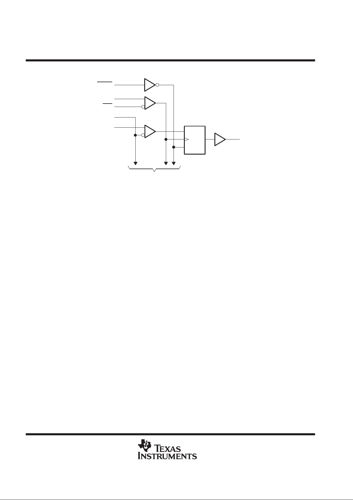
FUNCTION TABLE
(each flip-flop)
INPUTS
OUTPUT
RESET CLK CLK D
Q
L X X X L
H ↓↑HH
H ↓↑LL
H L or H L or H X Q
0
Copyright 1999, Texas Instruments Incorporated
Widebus is a trademark of Texas Instruments Incorporated.
Please be aware that an important notice concerning availability, standard warranty, and use in critical applications of
Texas Instruments semiconductor products and disclaimers thereto appears at the end of this data sheet.
PRODUCTION DATA information is current as of publication date.
Products conform to specifications per the terms of Texas Instruments
standard warranty. Production processing does not necessarily include
testing of all parameters.
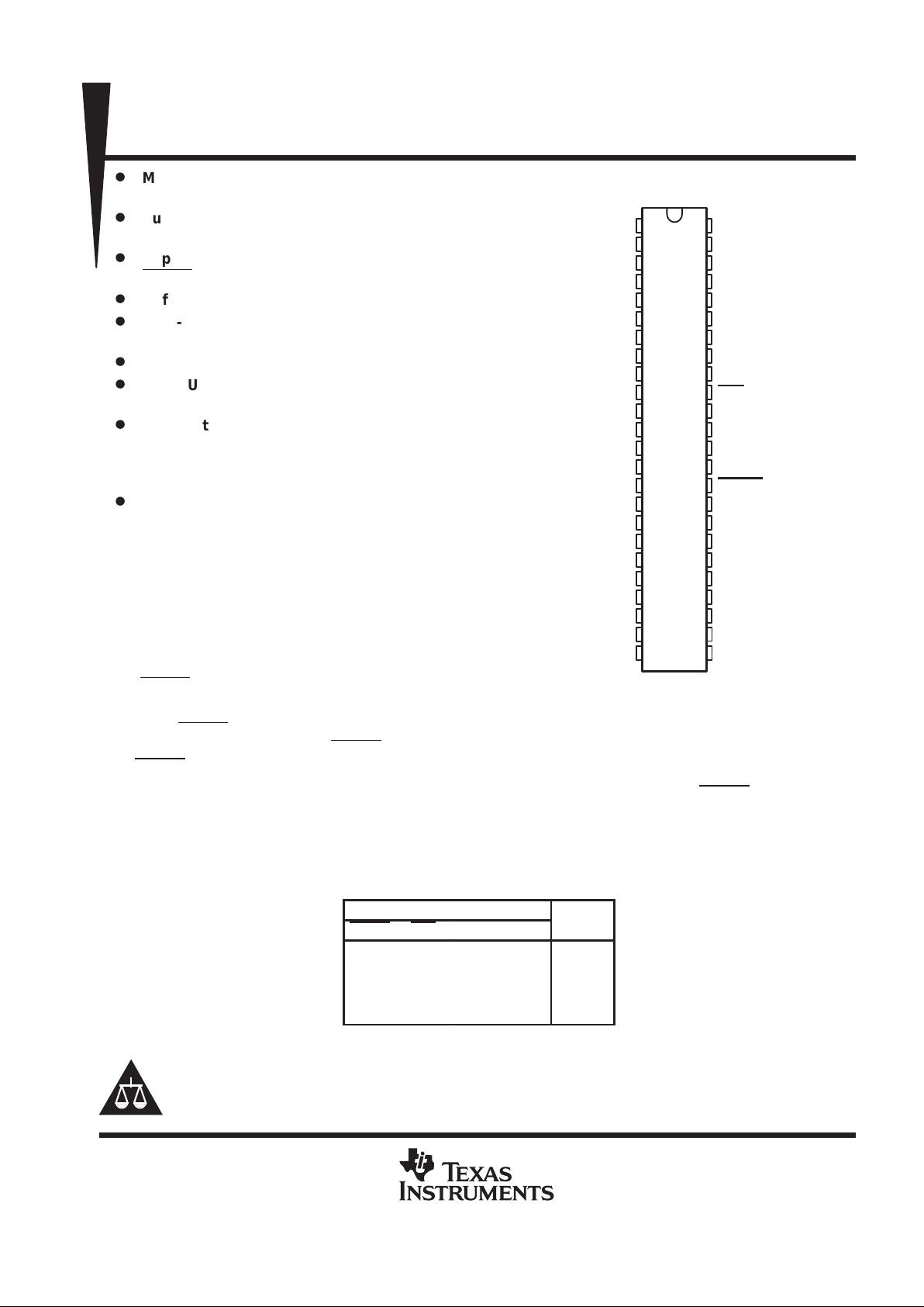
DGG PACKAGE
(TOP VIEW)
1
2
3
4
5
6
7
8
9
10
11
12
13
14
15
16
17
18
19
20
21
22
23
24
48
47
46
45
44
43
42
41
40
39
38
37
36
35
34
33
32
31
30
29
28
27
26
25
Q1
Q2
GND
V
DDQ
Q3
Q4
Q5
GND
V
DDQ
Q6
Q7
V
DDQ
GND
Q8
Q9
V
DDQ
GND
Q10
Q11
Q12
V
DDQ
GND
Q13
Q14
D1
D2
GND
V
CC
D3
D4
D5
D6
D7
CLK
CLK
V
CC
GND
V
REF
RESET
D8
D9
D10
D11
D12
V
CC
GND
D13
D14
Page 2
SN74SSTL16857
14-BIT SSTL_2 REGISTERED BUFFER
SCAS625C – FEBRUARY 1999 – REVISED OCTOBER 1999
2
POST OFFICE BOX 655303 • DALLAS, TEXAS 75265
logic diagram (positive logic)
1D
C1
R
To 13 Other Channels
34
1
RESET
Q1
39
CLK
38
CLK
35
V
REF
48
D1
absolute maximum ratings over operating free-air temperature range (unless otherwise noted)
†
Supply voltage range, VCC or V
DDQ
–0.5 V to 4.6 V. . . . . . . . . . . . . . . . . . . . . . . . . . . . . . . . . . . . . . . . . . . . . . . . .
Input voltage range, VI (see Note 1) –0.5 V to V
DDQ
+ 0.5 V. . . . . . . . . . . . . . . . . . . . . . . . . . . . . . . . . . . . . . . . .
Output voltage range, VO (see Notes 1 and 2) –0.5 V to V
DDQ
+ 0.5 V. . . . . . . . . . . . . . . . . . . . . . . . . . . . . . . .
Input clamp current, IIK (VI < 0) –50 mA. . . . . . . . . . . . . . . . . . . . . . . . . . . . . . . . . . . . . . . . . . . . . . . . . . . . . . . . . . .
Output clamp current, IOK (VO < 0) –50 mA. . . . . . . . . . . . . . . . . . . . . . . . . . . . . . . . . . . . . . . . . . . . . . . . . . . . . . . .
Continuous output current, I
O
(VO = 0 to V
DDQ
) ±50 mA. . . . . . . . . . . . . . . . . . . . . . . . . . . . . . . . . . . . . . . . . . . .
Continuous current through each VCC, V
DDQ
, or GND ±100 mA. . . . . . . . . . . . . . . . . . . . . . . . . . . . . . . . . . . . . .
Package thermal impedance, θJA (see Note 3) 70°C/W. . . . . . . . . . . . . . . . . . . . . . . . . . . . . . . . . . . . . . . . . . . . .
Storage temperature range, T
stg
–65°C to 150°C. . . . . . . . . . . . . . . . . . . . . . . . . . . . . . . . . . . . . . . . . . . . . . . . . . .
†
Stresses beyond those listed under “absolute maximum ratings” may cause permanent damage to the device. These are stress ratings only, and
functional operation of the device at these or any other conditions beyond those indicated under “recommended operating conditions” is not
implied. Exposure to absolute-maximum-rated conditions for extended periods may affect device reliability.
NOTES: 1. The input and output negative-voltage ratings may be exceeded if the input and output clamp-current ratings are observed.
2. Current flows only when the output is in the high state and VO > V
DDQ
.
3. The package thermal impedance is calculated in accordance with JESD 51.
Page 3
SN74SSTL16857
14-BIT SSTL_2 REGISTERED BUFFER
SCAS625C – FEBRUARY 1999 – REVISED OCTOBER 1999
3
POST OFFICE BOX 655303 • DALLAS, TEXAS 75265
recommended operating conditions (see Note 4)
MIN NOM MAX UNIT
V
CC
Supply voltage V
DDQ
3.6 V
V
DDQ
Output supply voltage 2.3 2.7 V
V
REF
Reference voltage (V
REF
= V
DDQ
/2) 1.15 1.25 1.35 V
V
TT
T ermination voltage V
REF
–40 mV V
REFVREF
+40 mV V
V
I
Input voltage 0 V
CC
V
V
IH
AC high-level input voltage Data inputs V
REF
+350 mV V
V
IL
AC low-level input voltage Data inputs V
REF
–350 mV V
V
IH
DC high-level input voltage Data inputs V
REF
+180 mV V
V
IL
DC low-level input voltage Data inputs V
REF
–180 mV V
V
IH
High-level input voltage RESET 2 V
V
IL
Low-level input voltage RESET 0.8 V
V
ICR
Common-mode input voltage range CLK, CLK 0.97 1.53 V
V
I(PP)
Peak-to-peak input voltage CLK, CLK 360 mV
I
OH
High-level output current –20 mA
I
OL
Low-level output current 20 mA
T
A
Operating free-air temperature 0 70
_
C
NOTE 4: All unused inputs of the device must be held at VCC or GND to ensure proper device operation. Refer to the TI application report,
Implications of Slow or Floating CMOS Inputs
, literature number SCBA004.
Page 4

SN74SSTL16857
14-BIT SSTL_2 REGISTERED BUFFER
SCAS625C – FEBRUARY 1999 – REVISED OCTOBER 1999
4
POST OFFICE BOX 655303 • DALLAS, TEXAS 75265
electrical characteristics over recommended operating free-air temperature range (unless
otherwise noted)
PARAMETER TEST CONDITIONS V
CC
MIN TYP MAX UNIT
V
IK
II = –18 mA 2.3 V –1.2 V
IOH = –100 µA 2.3 V to 2.7 V VCC–0.2
V
OH
IOH = –8 mA
1.95
V
IOH = –16 mA
2.3 V
1.95
IOL = 100 µA 2.3 V to 2.7 V 0.2
V
OL
IOL = 8 mA
0.35
V
IOL = 16 mA
2.3 V
0.35
VI = 1.7 V or 0.8V
±5
p
VI = 2.7 V or 0
V
REF
= 1.15 V or 1.35
V
2.7 V
±5
Data inputs
VI = 1.7 V or 0.8V
±5
µ
A
VI = 2.7 V or 0
V
REF
= 1.15 V or 1.35
V
3.6 V
±5
VI = 1.7 V or 0.8V
±1
VI = 2.7 V or 0
V
REF
= 1.15 V or 1.35
V
2.7 V
±1
I
I
CLK, CLK
VI = 1.7 V or 0.8V
±1
mA
VI = 2.7 V or 0
V
REF
= 1.15 V or 1.35
V
3.6 V
±1
2.7 V ±5
RESET
V
I
=
V
CC
or
GND
3.6 V ±5
2.7 V ±5
µ
A
V
REF
V
REF
= 1.15 V or 1.35
V
3.6 V ±5
VI = 1.7 V or 0.8 V
90
VI = 2.7 V or 0
I
O
=
0
2.7 V
90
I
CC
VI = 1.7 V or 0.8 V
90
mA
VI = 2.7 V or 0
I
O
=
0
3.6 V
90
RESET
3
Data inputs
V
I
=
1.7 V or 0.8 V
2.5 V
†
2.5
p
C
i
RESET
3
pF
Data inputs
V
I
= 1.7 V or 0.8
V
3.3 V
‡
2.5
†
All typical values are at VCC = 2.5 V, TA = 25°C.
‡
All typical values are at VCC = 3.3 V, TA = 25°C.
timing requirements over recommended operating free-air temperature range (unless otherwise
noted) (see Figure 1)
VCC = 2.5 V
± 0.2 V
VCC = 3.3 V
± 0.3 V
UNIT
MIN MAX MIN MAX
f
clock
Clock frequency 150 150 MHz
t
w
Pulse duration, CLK, CLK high or low 3.3 3.3 ns
p
Data before CLK↑, CLK↓ 1.1 1.75
tsuSetup time
RESET high before CLK↑, CLK↓ 0.6 1.1
ns
t
h
Hold time, data after CLK↑, CLK↓ 0.7 0.7 ns
Page 5

SN74SSTL16857
14-BIT SSTL_2 REGISTERED BUFFER
SCAS625C – FEBRUARY 1999 – REVISED OCTOBER 1999
5
POST OFFICE BOX 655303 • DALLAS, TEXAS 75265
switching characteristics over recommended operating free-air temperature range (unless
otherwise noted) (see Figure 1)
PARAMETER
FROM
TO
VCC = 2.5 V
± 0.2 V
VCC = 3.3 V
± 0.3 V
UNIT
(INPUT)
(OUTPUT)
MIN MAX MIN MAX
f
max
150 150 MHz
t
pd
CLK and CLK Q 1.5 3.8 1.4 3.7 ns
t
PHL
RESET
Q 1.5 4.3 1.4 3.5 ns
Page 6

SN74SSTL16857
14-BIT SSTL_2 REGISTERED BUFFER
SCAS625C – FEBRUARY 1999 – REVISED OCTOBER 1999
6
POST OFFICE BOX 655303 • DALLAS, TEXAS 75265
PARAMETER MEASUREMENT INFORMATION
V
CC
= 2.5 V ± 0.2 V AND VCC = 3.3 V ± 0.3 V
t
PHL
t
PLH
LOAD CIRCUIT
V
REF
†
V
IH
‡
V
IL
§
V
REF
†
V
REF
†
V
IH
‡
V
IL
§
V
IH
‡
V
IL
§
t
w
Input
VOLTAGE WAVEFORMS
SETUP AND HOLD TIMES
VOLTAGE WAVEFORMS
PROPAGATION DELAY TIMES
INVERTING AND NONINVERTING OUTPUTS
VOLTAGE WAVEFORMS
PULSE DURATION
Output
Waveform 1
(see Note B)
Output
Waveform 2
(see Note B)
V
OL
V
OH
t
PZL
t
PZH
t
PLZ
t
PHZ
V
REF
†
V
REF
†
V
TT
V
IL
§
V
IL
§
V
IH
‡
V
TT
V
IH
‡
Output
Control
V
REF
†
V
REF
†
V
IH
‡
V
IL
§
V
REF
†
V
REF
†
V
OH
V
OL
Input
Output
25 Ω
CL= 30 pF
(see Note A)
Test
Point
V
TT
V
REF
†
25 Ω
VOLTAGE WAVEFORMS
ENABLE AND DISABLE TIMES
LOW- AND HIGH-LEVEL ENABLING
V
IL
§
V
IH
‡
†
V
REF
= V
DDQ
/2
‡
VIH = V
REF
+ 350 mV (AC voltage levels)
§
VIL = V
REF
– 350 mV (AC voltage levels)
NOTES: A. CL includes probe and jig capacitance.
B. Waveform 1 is for an output with internal conditions such that the output is low except when disabled by the output control.
Waveform 2 is for an output with internal conditions such that the output is high except when disabled by the output control.
C. All input pulses are supplied by generators having the following characteristics: PRR ≤ 10 MHz, ZO = 50 Ω, tr ≤ 1.25 ns/V,
tf ≤ 1.25 ns/V.
D. The outputs are measured one at a time with one transition per measurement.
E. VTT = V
REF
= V
DDQ
/2
F. t
PLZ
and t
PHZ
are the same as t
dis
.
G. t
PZL
and t
PZH
are the same as ten.
H. t
PLH
and t
PHL
are the same as tpd.
Timing
Input
Data
Input
V
REF
†
t
su
t
h
Figure 1. Load Circuit and Voltage Waveforms
Page 7

IMPORTANT NOTICE
T exas Instruments and its subsidiaries (TI) reserve the right to make changes to their products or to discontinue
any product or service without notice, and advise customers to obtain the latest version of relevant information
to verify, before placing orders, that information being relied on is current and complete. All products are sold
subject to the terms and conditions of sale supplied at the time of order acknowledgement, including those
pertaining to warranty, patent infringement, and limitation of liability.
TI warrants performance of its semiconductor products to the specifications applicable at the time of sale in
accordance with TI’s standard warranty. Testing and other quality control techniques are utilized to the extent
TI deems necessary to support this warranty. Specific testing of all parameters of each device is not necessarily
performed, except those mandated by government requirements.
CERT AIN APPLICATIONS USING SEMICONDUCTOR PRODUCTS MAY INVOLVE POTENTIAL RISKS OF
DEATH, PERSONAL INJURY, OR SEVERE PROPERTY OR ENVIRONMENTAL DAMAGE (“CRITICAL
APPLICATIONS”). TI SEMICONDUCTOR PRODUCTS ARE NOT DESIGNED, AUTHORIZED, OR
WARRANTED TO BE SUITABLE FOR USE IN LIFE-SUPPORT DEVICES OR SYSTEMS OR OTHER
CRITICAL APPLICATIONS. INCLUSION OF TI PRODUCTS IN SUCH APPLICA TIONS IS UNDERSTOOD T O
BE FULLY AT THE CUSTOMER’S RISK.
In order to minimize risks associated with the customer’s applications, adequate design and operating
safeguards must be provided by the customer to minimize inherent or procedural hazards.
TI assumes no liability for applications assistance or customer product design. TI does not warrant or represent
that any license, either express or implied, is granted under any patent right, copyright, mask work right, or other
intellectual property right of TI covering or relating to any combination, machine, or process in which such
semiconductor products or services might be or are used. TI’s publication of information regarding any third
party’s products or services does not constitute TI’s approval, warranty or endorsement thereof.
Copyright 1999, Texas Instruments Incorporated
 Loading...