

Page 1
SN74S225
16 × 5 ASYNCHRONOUS FIRST-IN, FIRST-OUT MEMORY
WITH 3-STATE OUTPUTS
SDLS207B – SEPTEMBER 1976 – REVISED APRIL 1998
1
POST OFFICE BOX 655303 • DALLAS, TEXAS 75265
D
Independent Asychronous Inputs and
Outputs
D
16 Words by 5 Bits
D
DC to 10-MHz Data Rate
D
3-State Outputs
D
Packaged in Standard Plastic 300-mil DIPs
description
This 80-bit active-element memory is a monolithic
Schottky-clamped transistor-transistor logic
(STTL) array organized as 16 words by 5 bits. A
memory system using the SN74S225 easily can
be expanded in multiples of 48 words or of 10 bits
as shown in Figure 3. The 3-state outputs
controlled by a single output-enable (OE
) input
make bus connection and multiplexing easy.
A first-in, first-out (FIFO) memory is a storage device that allows data to be written into and read from its array
at independent data rates. This FIFO is designed to process data at rates from dc to 10 MHz in a bit-parallel
format, word by word.
Reading or writing is done independently , utilizing separate asynchronous data clocks. Data can be written into
the array on the low-to-high transition of either load-clock (CLKA, CLKB) input. Data can be read out of the array
on the low-to-high transition of the unload-clock (UNCK IN) input (normally high). Writing data into the FIFO can
be accomplished in one of two ways:
D
In applications not requiring a gated clock control, best results are achieved by applying the clock input to
one of the clocks while tying the other clock input high.
D
In applications needing a gated clock, the load clock (gate control) must be high for the FIFO to load on the
next clock pulse.
CLKA and CLKB can be used interchangeably for either clock gate control or clock input.
Status of the SN74S225 is provided by three outputs. The input-ready (IR) output monitors the status of the last
word location and signifies when the memory is full. This output is high whenever the memory is available to
accept any data. The unload-clock (UNCK OUT) output also monitors the last word location. This output
generates a low-logic-level pulse (synchronized to the internal clock pulse) when the location is vacant. The third
status output, output ready (OR), is high when the first word location contains valid data and UNCK IN is high.
When UNCK IN goes low, OR will go low and stay low until new valid data is in the first word position. The first
word location is defined as the location from which data is provided to the outputs.
The data outputs are noninverted with respect to the data inputs and are 3-state, with a common control input
(OE
). When OE is low, the data outputs are enabled to function as totem-pole outputs. A high logic level forces
each data output to a high-impedance state while all other inputs and outputs remain active.The clear (CLR
)
input invalidates all data stored in the memory array by clearing the control logic and setting OR to a low logic
level on the high-to-low transition of a low-active pulse.
The SN74S225 is characterized for operation from 0°C to 70°C.
Copyright 1998, Texas Instruments Incorporated
PRODUCTION DATA information is current as of publication date.
Products conform to specifications per the terms of Texas Instruments
standard warranty. Production processing does not necessarily include
testing of all parameters.
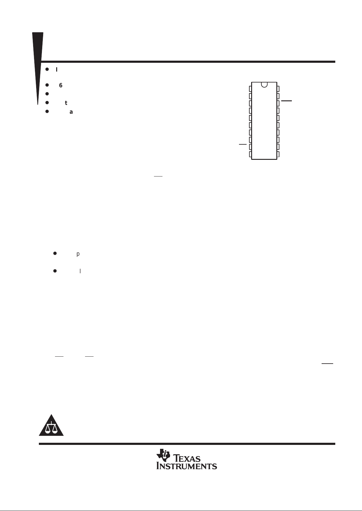
1
2
3
4
5
6
7
8
9
10
20
19
18
17
16
15
14
13
12
11
CLKA
IR
UNCK OUT
D0
D1
D2
D3
D4
OE
GND
V
CC
CLKB
CLR
OR
UNCK IN
Q0
Q1
Q2
Q3
Q4
N PACKAGE
(TOP VIEW)
Please be aware that an important notice concerning availability, standard warranty, and use in critical applications of
Texas Instruments semiconductor products and disclaimers thereto appears at the end of this data sheet.
Page 2
SN74S225
16 × 5 ASYNCHRONOUS FIRST -IN, FIRST-OUT MEMORY
WITH 3-STATE OUTPUTS
SDLS207B – SEPTEMBER 1976 – REVISED APRIL 1998
2
POST OFFICE BOX 655303 • DALLAS, TEXAS 75265
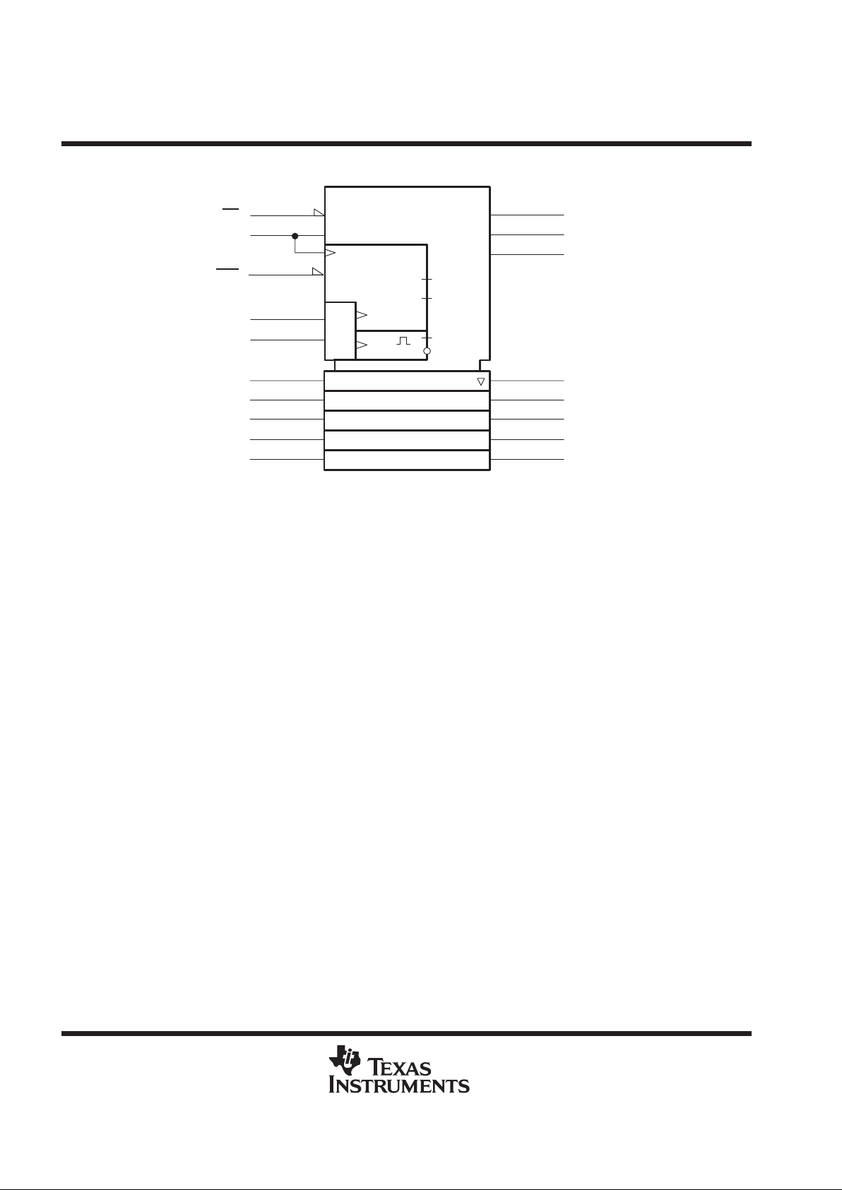
logic symbol
†
EN6
9
4D
4
D0 Q0
15
5
D1
Q1
14
6
D2
Q2
13
7
D3
Q3
12
8
D4
Q4
11
Z1
16
UNCK IN
FIFO 16 × 5
OE
6
CT = 0
18
CLR
UNCK OUT
3
2
IR
2
5, 2
OR
17
1, 3
1
CLKA
19
CLKB
3–
2+
2
&
CTR
G2
G3
C4
Z5
CT < 16
CT > 0
1
†
This symbol is in accordance with ANSI/IEEE Standard 91-1984 and IEC Publication 617-12.
Page 3
SN74S225
16 × 5 ASYNCHRONOUS FIRST-IN, FIRST-OUT MEMORY
WITH 3-STATE OUTPUTS
SDLS207B – SEPTEMBER 1976 – REVISED APRIL 1998
3
POST OFFICE BOX 655303 • DALLAS, TEXAS 75265
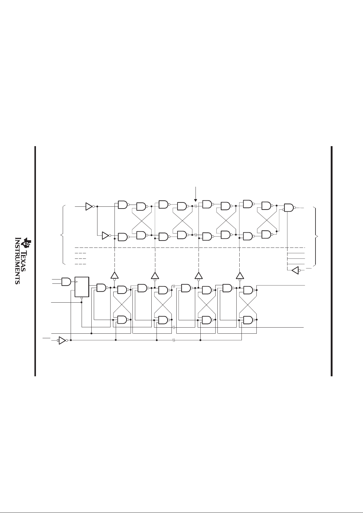
D0
D1
D2
D3
D4
CLKA
CLKB
UNCK
IR
CLR
OUT
Q0
Q1
Q2
Q3
Q4
OE
OR
UNCK
IN
Data Inputs
Data Outputs
4
5
6
7
8
1
19
3
2
18
C1
1D
R
Word 16
(last word)
Word 1
(first word)
Word 2Word 15
Words 3 – 14
Same as 2 or 15
Same as D10
Same as Q0
15
14
13
12
11
9
17
16
functional block diagram
Page 4

SN74S225
16 × 5 ASYNCHRONOUS FIRST -IN, FIRST-OUT MEMORY
WITH 3-STATE OUTPUTS
SDLS207B – SEPTEMBER 1976 – REVISED APRIL 1998
4
POST OFFICE BOX 655303 • DALLAS, TEXAS 75265
schematics of inputs and outputs
V
CC
Input
EQUIVALENT OF ALL INPUTS
EXCEPT DATA INPUTS
V
CC
Input
EQUIVALENT OF
DATA INPUTS
58 Ω NOM
V
CC
Output
TYPICAL OF
ALL OUTPUTS
absolute maximum ratings over operating free-air temperature range (unless otherwise noted)
†
Supply voltage range, V
CC
(see Note 1) –0.5 V to 7 V. . . . . . . . . . . . . . . . . . . . . . . . . . . . . . . . . . . . . . . . . . . . . .
Input voltage range, V
I
–0.5 V to 5.5 V. . . . . . . . . . . . . . . . . . . . . . . . . . . . . . . . . . . . . . . . . . . . . . . . . . . . . . . . . . . . .
Off-state output voltage range –0.5 V to 5.5 V. . . . . . . . . . . . . . . . . . . . . . . . . . . . . . . . . . . . . . . . . . . . . . . . . . . . . .
Package thermal impedance, θ
JA
(see Note 2) 67°C/W. . . . . . . . . . . . . . . . . . . . . . . . . . . . . . . . . . . . . . . . . . . . .
Storage temperature range, T
stg
–65°C to 150°C. . . . . . . . . . . . . . . . . . . . . . . . . . . . . . . . . . . . . . . . . . . . . . . . . . .
†
Stresses beyond those listed under “absolute maximum ratings” may cause permanent damage to the device. These are stress ratings only, and
functional operation of the device at these or any other conditions beyond those indicated under “recommended operating conditions” is not
implied. Exposure to absolute-maximum-rated conditions for extended periods may affect device reliability.
NOTES: 1. All voltage values are with respect to GND.
2. The package thermal impedance is calculated in accordance with JESD 51, except for through-hole packages, which use a trace
length of zero.
Page 5

SN74S225
16 × 5 ASYNCHRONOUS FIRST -IN, FIRST-OUT MEMORY
WITH 3-STATE OUTPUTS
SDLS207B – SEPTEMBER 1976 – REVISED APRIL 1998
5
POST OFFICE BOX 655303 • DALLAS, TEXAS 75265
recommended operating conditions
MIN NOM MAX UNIT
V
CC
Supply voltage 4.75 5 5.25 V
V
IH
High-level input voltage 2 V
V
IL
Low-level input voltage 0.8 V
p
Q outputs –6.5
IOHHigh-level output current
All other outputs –3.2
mA
p
Q outputs 16
IOLLow-level output current
All other outputs 8
mA
T
A
Operating free-air temperature 0 70 °C
electrical characteristics over recommended operating free-air temperature range (unless
otherwise noted)
PARAMETER TEST CONDITIONS MIN TYP†MAX UNIT
V
IK
VCC = 4.75 V , II = –18 mA –1.2 V
Q outputs VCC = 4.75 V , IOL = –6.5 mA 2.4 2.9
V
OH
All others VCC = 4.75 V , IOL = –3.2 mA 2.4 2.9
V
Q outputs VCC = 4.75 V , IOL = 16 mA 0.35 0.5
V
OL
All others VCC = 4.75 V , IOL = 8 mA 0.35 0.5
V
I
OZH
VCC = 5.25 V , VO = 2.4 V 50 µA
I
OZL
VCC = 5.25 V , VO = 0.5 V –50 µA
I
I
VCC = 5.25 V , VI = 5.5 V 1 mA
Data
40
I
IH
All others
V
CC
= 5.25 V,
V
I
= 2.7
V
25
µ
A
Data
–1
I
IL
All others
V
CC
= 5.25 V,
V
I
= 0.5
V
–0.25
mA
I
OS
‡
VCC = 5.25 V , VO = 0 –30 –100 mA
I
CC
§
VCC = 5.25 V 80 120 mA
†
All typical values are at VCC = 5 V, TA = 25°C.
‡
Duration of the short circuit should not exceed one second.
§
ICC is measured with all inputs grounded and the outputs open.
timing requirements over recommended operating conditions (unless otherwise noted) (see
Figure 1)
MIN NOM MAX UNIT
f
clock
Clock frequency 10 MHz
CLKA or CLKB high 25
t
w
Pulse duration
UNCK IN low 7
ns
CLR low 40
Data (see Note 3) –20
t
su
S
etup time before
CLKA↑
or
CLKB↑
CLR inactive 25
ns
t
h
Hold time after CLKA↑ or CLKB↑ 70 ns
NOTE 3: Data must be set up within 20 ns after the load-clock positive transition.
Page 6

SN74S225
16 × 5 ASYNCHRONOUS FIRST -IN, FIRST-OUT MEMORY
WITH 3-STATE OUTPUTS
SDLS207B – SEPTEMBER 1976 – REVISED APRIL 1998
6
POST OFFICE BOX 655303 • DALLAS, TEXAS 75265
switching characteristics over recommended ranges of supply voltage and operating free-air
temperature (unless otherwise noted) (see Figure 1)
PARAMETER
FROM
(INPUT)
TO
(OUTPUT)
TEST CONDITIONS MIN TYP†MAX UNIT
CLKA 10 20
f
max
CLKB
CL = 30 pF
10 20
MHz
UNCK IN 10 20
t
w
UNCK OUT CL = 30 pF 7 14 ns
t
dis
OE
Any Q CL = 5 pF 10 25 ns
t
en
OE
Any Q CL = 30 pF 25 40 ns
t
PLH
p
50 75
t
PHL
UNCK IN
A
ny
Q
C
L
=
30 pF
50 75
ns
t
PLH
CLKA or CLKB OR CL = 30 pF 190 300 ns
t
PLH
p
40 60
t
PHL
UNCK IN
OR
C
L
= 30
pF
30 45
ns
CLR OR 35 60
CLKA or CLKB
p
25 45
t
PHL
UNCK IN
UNCK OUT
C
L
= 30
pF
270 400
ns
CLKA or CLKB IR 55 75
UNCK IN
255 400
t
PLH
CLR
IR
CL = 30 pF
16 35
ns
OR↑
Any Q
10 20
†
All typical values are at VCC = 5 V, TA = 25°C.
Page 7

SN74S225
16 × 5 ASYNCHRONOUS FIRST -IN, FIRST-OUT MEMORY
WITH 3-STATE OUTPUTS
SDLS207B – SEPTEMBER 1976 – REVISED APRIL 1998
7
POST OFFICE BOX 655303 • DALLAS, TEXAS 75265
PARAMETER MEASUREMENT INFORMATION
t
PHZ
t
PLZ
0.3 V
t
PZL
t
PZH
LOAD CIRCUIT FOR 3-STATE OUTPUTS
From Output
Under Test
Test Point
R1 = 500 Ω
S1
C
L
(see Note A)
7 V
Open
1.3 V
1.3 V1.3 V
3.5 V
3.5 V
0.3 V
0.3 V
t
h
t
su
VOLTAGE WAVEFORMS
SET UP AND HOLD TIMES
Timing
Input
Data
Input
1.3 V 1.3 V
3.5 V
3.5 V
0.3 V
0.3 V
High-Level
Pulse
Low-Level
Pulse
VOLTAGE WAVEFORMS
PULSE DURATION
1.3 V1.3 V
1.3 V
1.3 V
3.5 V
0.3 V
Output
Control
Waveform 1
S1 Closed
(see Note B)
Waveform 2
S1 Open
(see Note B)
0 V
V
OH
V
OL
3.5 V
0.3 V
1.3 V
1.3 V
VOLTAGE WAVEFORMS
ENABLE AND DISABLE TIMES, 3-STATE OUTPUTS
R2 = 500 Ω
t
w
t
PZH
t
PZL
t
PHZ
t
PLZ
t
PLH
t
PHL
Open
Closed
Open
Closed
Open
Open
PARAMETER S1
t
en
t
dis
t
pd
t
PHL
t
PLH
t
PLH
t
PHL
Input
(see Note C)
Out-of-Phase
Output
1.3 V 1.3 V
1.3 V1.3 V
1.3 V 1.3 V
3.5 V
0.3 V
V
OL
V
OH
V
OH
V
OL
In-Phase
Output
VOLTAGE WAVEFORMS
PROPAGATION DELAY TIMES
NOTES: A. CL includes probe and jig capacitance.
B. Waveform 1 is for an output with internal conditions such that the output is low except when disabled by the output control.
Waveform 2 is for an output with internal conditions such that the output is high except when disabled by the output control.
C. All input pulses are supplied by generators having the following characteristics: PRR ≤ 1 MHz, Zo = 50 Ω, tr ≤ 2 ns, tf≤ 2 ns.
D. The outputs are measured one at a time with one transition per measurement.
Figure 1. Load Circuit and Voltage Waveforms
Page 8

SN74S225
16 × 5 ASYNCHRONOUS FIRST -IN, FIRST-OUT MEMORY
WITH 3-STATE OUTPUTS
SDLS207B – SEPTEMBER 1976 – REVISED APRIL 1998
8
POST OFFICE BOX 655303 • DALLAS, TEXAS 75265
APPLICATION INFORMATION
CLR
CLKA
CLKB
D
Word 1 Word 2 Word 16
UNCK
IN
IR
UNCK
OUT
OR
Q
Word 3
is Low
Word 1 Word 1 W ord 2 Word 3 Word
16
Load
Words 3–15
Unload
Word 16
Outputs Inputs
Clear Load
Word 1
Load
Word 2
Load
Word 16
Unload
Word 2
Unload
Word 1
Unload
Words 3–15
Figure 2. Typical Waveforms for a 16-Word FIFO
Page 9

SN74S225
16 × 5 ASYNCHRONOUS FIRST -IN, FIRST-OUT MEMORY
WITH 3-STATE OUTPUTS
SDLS207B – SEPTEMBER 1976 – REVISED APRIL 1998
9
POST OFFICE BOX 655303 • DALLAS, TEXAS 75265
APPLICATION INFORMATION
UNCK
IR
D0
D1
D2
D3
UNCK
OR
Q0
Q1
Q2
Q3
CLR
IR
D4
OE
Q4
OUT
IN
CLKB
CLKA
(high)
UNCK
IR
D0
D1
D2
D3
UNCK
OR
Q0
Q1
Q2
Q3
CLR
D4
OE
Q4
OUT
IN
CLKB
CLKA
(high)
UNCK
IR
D0
D1
D2
D3
UNCK
OR
Q0
Q1
Q2
Q3
CLR
D4
OE
Q4
OUT
IN
CLKB
CLKA
UNCK
IR
D0
D1
D2
D3
UNCK
OR
Q0
Q1
Q2
Q3
CLR
D4
OE
Q4
OUT
IN
CLKB
CLKA
UNCK
IR
D0
D1
D2
D3
UNCK
OR
Q0
Q1
Q2
Q3
CLR
D4
OE
Q4
OUT
IN
CLKB
CLKA
UNCK
IR
D0
D1
D2
D3
UNCK
OR
Q0
Q1
Q2
Q3
CLR
D4
OE
Q4
OUT
IN
CLKB
CLKA
(high)
(high)
(high)
(high)
NC NC
NC NC
NC
CLR
NC
CLK
OR
UNCK IN
OE
5-Bit
Data
In
5-Bit
Data
Out
5-Bit
Data
In
5-Bit
Data
Out
Figure 3. Word-Width Expansion: 48 × 10 Bits
Page 10

IMPORTANT NOTICE
T exas Instruments and its subsidiaries (TI) reserve the right to make changes to their products or to discontinue
any product or service without notice, and advise customers to obtain the latest version of relevant information
to verify, before placing orders, that information being relied on is current and complete. All products are sold
subject to the terms and conditions of sale supplied at the time of order acknowledgement, including those
pertaining to warranty, patent infringement, and limitation of liability.
TI warrants performance of its semiconductor products to the specifications applicable at the time of sale in
accordance with TI’s standard warranty. Testing and other quality control techniques are utilized to the extent
TI deems necessary to support this warranty. Specific testing of all parameters of each device is not necessarily
performed, except those mandated by government requirements.
CERT AIN APPLICATIONS USING SEMICONDUCTOR PRODUCTS MA Y INVOLVE POTENTIAL RISKS OF
DEATH, PERSONAL INJURY, OR SEVERE PROPERTY OR ENVIRONMENTAL DAMAGE (“CRITICAL
APPLICATIONS”). TI SEMICONDUCTOR PRODUCTS ARE NOT DESIGNED, AUTHORIZED, OR
WARRANTED TO BE SUITABLE FOR USE IN LIFE-SUPPORT DEVICES OR SYSTEMS OR OTHER
CRITICAL APPLICATIONS. INCLUSION OF TI PRODUCTS IN SUCH APPLICA TIONS IS UNDERST OOD TO
BE FULLY AT THE CUSTOMER’S RISK.
In order to minimize risks associated with the customer’s applications, adequate design and operating
safeguards must be provided by the customer to minimize inherent or procedural hazards.
TI assumes no liability for applications assistance or customer product design. TI does not warrant or represent
that any license, either express or implied, is granted under any patent right, copyright, mask work right, or other
intellectual property right of TI covering or relating to any combination, machine, or process in which such
semiconductor products or services might be or are used. TI’s publication of information regarding any third
party’s products or services does not constitute TI’s approval, warranty or endorsement thereof.
Copyright 1999, Texas Instruments Incorporated
 Loading...