

Page 1
SN54LVT8980, SN74LVT8980
EMBEDDED TEST-BUS CONTROLLERS
IEEE STD 1149.1 (JTAG) TAP MASTERS WITH 8-BIT GENERIC HOST INTERFACES
SCBS676C – DECEMBER 1996 – REVISED AUGUST 1997
D
Members of Texas Instruments (TI) Broad
Family of Testability Products Supporting
IEEE Std 1149.1-1990 (JTAG) Test Access
Port (TAP) and Boundary-Scan Architecture
D
Provide Built-In Access to IEEE Std 1149.1
Scan-Accessible Test/Maintenance
Facilities at Board and System Levels
D
While Powered at 3.3 V, the TAP Interface is
Fully 5-V Tolerant for Mastering Both 5-V
and/or 3.3-V IEEE Std 1149.1 Targets
D
Simple Interface to Low-Cost 3.3-V
Microprocessors/Microcontrollers Via 8-Bit
Asynchronous Read/Write Data Bus
D
Easy Programming Via Scan-Level
Command Set and Smart TAP Control
D
Transparently Generate Protocols to
Support Multidrop TAP Configurations
Using TI’s Addressable Scan Port
D
Flexible TCK Generator Provides
Programmable Division, Gated-TCK, and
Free-Running-TCK Modes
D
Discrete TAP Control Mode Supports
Arbitrary TMS/TDI Sequences for
Non-Compliant Targets
D
Programmable 32-Bit T est Cycle Counter
Allows Virtually Unlimited Scan/Test Length
D
Accommodate Target Retiming (Pipeline)
Delays of Up to 15 TCK Cycles
D
Test Output Enable (TOE) Allows for
External Control of TAP Signals
D
High-Drive Outputs (–32-mA IOH, 64-mA IOL)
at TAP Support Backplane Interface and/or
High Fanout
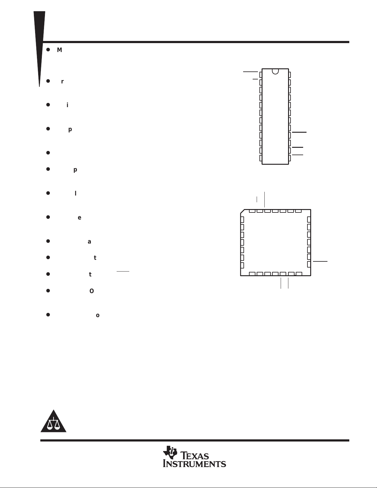
D
Package Options Include Plastic
Small-Outline (DW) Package, Ceramic Chip
Carriers (FK), and Ceramic 300-mil DIPs (JT)
SN54LVT8980...JT PACKAGE
SN74LVT8980. . . DW PACKAGE
STRB
CLKIN
SN54LVT8980. . . FK PACKAGE
D1
D2
D3
NC
GND
D4
D5
NC – No internal connection
(TOP VIEW)
1
R/W
2
D0
3
D1
4
D2
5
D3
6
GND
7
D4
8
D5
9
D6
10
D7
11
12
(TOP VIEW)
D0
R/W
STRB
4 3 2 128
5
6
7
8
9
10
11
12 13 14 15 16 17 18
D7
D6
CLKIN
NC
NC
24
23
22
21
20
19
18
17
16
15
14
13
A0
27 26
TOE
A0
A1
A2
RDY
TDO
V
CC
TCK
TMS
TRST
TDI
RST
TOE
A1
A2
25
24
23
22
21
20
19
TDI
RST
RDY
TDO
V
CC
NC
TCK
TMS
TRST
description
The ’L VT8980 embedded test-bus controllers (eTBC) are members of the TI broad family of testability integrated
circuits. This family of devices supports IEEE Std 1149.1-1990 boundary scan to facilitate testing of complex
circuit assemblies. Unlike most other devices of this family, the eTBC is not a boundary-scannable device;
rather, its function is to master an IEEE Std 1149.1 (JTAG) test access port (TAP) under the command of an
embedded host microprocessor/microcontroller. Thus, the eTBC enables the practical and ef fective use of the
IEEE Std 1149.1 test-access infrastructure to support embedded/built-in test, emulation, and
configuration/maintenance facilities at board and system levels.
Please be aware that an important notice concerning availability, standard warranty, and use in critical applications of
Texas Instruments semiconductor products and disclaimers thereto appears at the end of this data sheet.
UNLESS OTHERWISE NOTED this document contains PRODUCTION
DATA information current as of publication date. Products conform to
specifications per the terms of Texas Instruments standard warranty.
Production processing does not necessarily include testing of all
parameters.
POST OFFICE BOX 655303 • DALLAS, TEXAS 75265
Copyright 1997, Texas Instruments Incorporated
1
Page 2

SN54LVT8980, SN74LVT8980
EMBEDDED TEST-BUS CONTROLLERS
IEEE STD 1149.1 (JTAG) TAP MASTERS WITH 8-BIT GENERIC HOST INTERFACES
SCBS676C – DECEMBER 1996 – REVISED AUGUST 1997
description (continued)
The eTBC masters all T AP signals required to support one 4- or 5-wire IEEE Std 1149.1 serial test bus – test
clock (TCK), test mode select (TMS), test data input (TDI), test data output (TDO), and test reset (TRST). All
such signals can be connected directly to the associated target IEEE Std 1149.1 devices without need for
additional logic or buffering. However , as well as being directly connected, the TMS, TDI, and TDO signals can
be connected to distant target IEEE Std 1149.1 devices via a pipeline, with a retiming delay of up to 15 TCK
cycles; the eTBC automatically handles all associated serial-data justification.
Conceptually, the eTBC operates as a simple 8-bit memory- or I/O- mapped peripheral to a
microprocessor/microcontroller (host). High-level commands and parallel data are passed to/from the eTBC via
its generic host interface, which includes an 8-bit data bus (D7–D0) and a 3-bit address bus (A2–A0). Read/write
select (R/W
of the CLKIN period. An asynchronous ready (RDY) indicator is provided to hold off, or insert wait states into,
a host read/write cycle when the eTBC cannot respond immediately to the requested read/write operation.
High-level commands are issued by the host to cause the eTBC to generate the TMS sequences necessary
to move the test bus from any stable T AP-controller state to any other such stable state, to scan instruction or
data through test registers in target devices, and/or to execute instructions in the Run-Test/Idle TAP state. A
32-bit counter can be programmed to allow a predetermined number of scan or execute cycles.
During scan operations, serial data that appears at the TDI input is transferred into a serial-to-4 × 8-bit-parallel
first-in/first-out (FIFO) read buffer, which can then be read by the host to obtain the return serial-data stream
up to eight bits at a time. Serial data that is to be transmitted from the TDO output is written by the host, up to
eight bits at a time, to a 4 × 8-bit-parallel-to-serial FIFO write buffer.
) and strobe (STRB) signals are implemented so that the critical host-interface timing is independent
In addition to such simple state-movement, scan, and run-test operations, the eTBC supports several additional
commands that provide for input-only scans, output-only scans, recirculate scans (in which TDI is mirrored back
to TDO), and a scan mode that generates the protocols used to support multidrop T AP configurations using TI’s
addressable scan port. Two loopback modes also are supported that allow the microprocessor/microcontroller
host to monitor the TDO or TMS data streams output by the eTBC.
The eTBC’s flexible clocking architecture allows the user to choose between free-running (in which the TCK
always follows CLKIN) and gated modes (in which the TCK output is held static except during state-move,
run-test, or scan cycles) as well as to divide down TCK from CLKIN. A discrete mode is also available in which
the TAP is driven strictly by read/write cycles under full control of the microprocessor/microcontroller host.
These features ensure that virtually any IEEE Std 1 149.1 target device or device chain – even where such may
not fully comply to IEEE Std 1149.1 – can be serviced by the eTBC.
While most operations of the eTBC are synchronous to CLKIN, a test-output enable (TOE
control of the T AP outputs, and a reset (RST) input is provided for hardware reset of the eTBC. The former can
be used to disable the eTBC so that an external controller can master the associated IEEE Std 1 149.1 test bus.
The SN54LVT8980 is characterized for operation over the full military temperature range of –55°C to 125°C.
The SN74LVT8980 is characterized for operation from –40°C to 85°C.
) is provided for output
2
POST OFFICE BOX 655303 • DALLAS, TEXAS 75265
Page 3
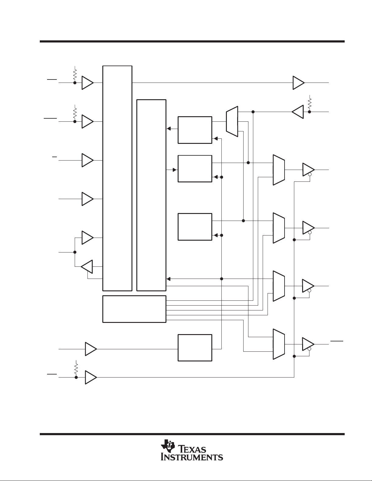
IEEE STD 1149.1 (JTAG) TAP MASTERS WITH 8-BIT GENERIC HOST INTERFACES
functional block diagram
V
CC
SN54LVT8980, SN74LVT8980
EMBEDDED TEST-BUS CONTROLLERS
SCBS676C – DECEMBER 1996 – REVISED AUGUST 1997
STRB
R/W
A2–A0
D7–D0
14
1
2
22–24
11–8,
6–3
21
RDYRST
V
CC
V
CC
15
TDI
TDI
Buffer
Host
Interface
Command/
Control
TDO
Buffer
TAP-State
Generator
20
17
TDO
TMS
Discrete Control
12
CLKIN
V
CC
13
TOE
Pin numbers shown are for the DW and JT packages.
TCK
Generator
18
16
TCK
TRST
POST OFFICE BOX 655303 • DALLAS, TEXAS 75265
3
Page 4
SN54LVT8980, SN74LVT8980
EMBEDDED TEST-BUS CONTROLLERS
IEEE STD 1149.1 (JTAG) TAP MASTERS WITH 8-BIT GENERIC HOST INTERFACES
SCBS676C – DECEMBER 1996 – REVISED AUGUST 1997
Terminal Functions
TERMINAL
NAME
A2–A0
CLKIN
D7–D0
GND Ground
RDY
RST
R/W
STRB
TCK
TDI
TDO
TMS
TOE
TRST
V
CC
DESCRIPTION
Address inputs. A2–A0 form the 3-bit address bus that interfaces the eTBC to its microprocessor/microcontroller host. These
inputs directly index the eTBC register to be accessed (read from or written to).
Clock input. CLKIN is the system clock input for the eTBC. Most operations of the eTBC are synchronous to CLKIN. Internally,
the CLKIN signal is divided by a programmable divisor to generate TCK.
Data inputs/outputs. D7–D0 form the 8-bit bidirectional data bus that interfaces the eTBC to its
microprocessor/microcontroller host. Data in the eTBC registers is accessed (read or written) using this data bus. D7 is
considered the most-significant bit, while D0 is considered the least-significant bit.
Ready output. RDY is used to indicate to the microprocessor/microcontroller host whether or not the eTBC is ready to service
the access (read or write) operation that is currently being requested. If RDY remains high following the initiation of an access
cycle (STRB
(STRB
may clear the not-ready state, which allows RDY to return high before the end of the access cycle. In any event, the RDY
output returns high upon the termination of any access cycle (STRB
Reset input. RST is used to initiate asynchronous reset of the eTBC. Assertion (low) of RST places the eTBC in a reset state
from which it does not exit until RST
and TRST
connection.
Read/write select. R/W is used by the microprocessor/microcontroller host to instruct the eTBC as to whether it is to perform
read access (R/W
drive low and/or high logic levels onto the host data bus. Otherwise, while R/W
high-impedance state so that the host data bus can drive to the eTBC.
Read/write strobe. STRB is used by the microprocessor/microcontroller host to instruct the eTBC to initiate (STRB negative
edge) or terminate/conclude (STRB
high level if it has no external connection.
Test clock. TCK transmits the TCK signal required by the eTBC’s IEEE Std 1149.1 target(s). All operations of the TAP are
synchronous to TCK. Generally, the TCK signal is generated internally by the eTBC by division of CLKIN by a programmable
divisor. Alternatively, when the eTBC is in its discrete-control mode, a rising edge of TCK is generated on a read to the
discrete-control register, while a falling edge is generated on a write to the discrete-control register.
Test data input. TDI receives the TDI signal output by the eTBC’s IEEE Std 1149.1 target(s). It is the serial input for shifting
test data from the target(s); it is sampled on the rising edge of TCK and is expected to be transferred from the target(s) on
the falling edge of TCK. An internal pullup forces TDI to a high level if it has no external connection.
Test data output. TDO transmits the TDO signal required by the eTBC’s IEEE Std 1149.1 target(s). It is the serial output for
shifting test data to the target(s); it is transferred on the falling edge of TCK and is sampled in the target on the rising edge
of TCK.
T est mode select. TMS transmits the TMS signal required by the eTBC’s IEEE Std 1 149.1 target(s). It is the one control signal
that directs the next TAP-controller state of the target(s). It is transferred from the eTBC on the falling edge of TCK and is
sampled in the target(s) on the rising edge of TCK.
T est-output enable. TOE is the active-low output enable for the eTBC TAP outputs (TCK, TDO, TMS, TRST). When TOE is
inactive (high) the TAP outputs are disabled to a high-impedance state. Otherwise, when TOE
are enabled to drive low and/or high logic levels according to other eTBC functions. An internal pullup forces TOE
level if it has no external connection.
Test reset. TRST transmits the TRST signal that may be required by some of the eTBC’s IEEE Std 1149.1 target(s). A low
signal at TRST
generated only when the microprocessor/microcontroller host writes an appropriate value into the eTBC command register
or, while the eTBC is in discrete-control mode, into the discrete-control register.
Supply voltage
negative edge) then the eTBC is ready. Otherwise, if RDY goes low following the initiation of an access cycle
negative edge) then the eTBC is not ready. In cases where the eTBC is not ready , subsequent processing in the eTBC
positive edge).
is released (high). While RST is low, the eTBC ignores host writes, the RDY, TDO, TMS,
outputs are high, while TCK outputs CLKIN/16. An internal pullup forces RST to a high level if it has no external
high) or write access (R/W low). While R/W is high and STRB is low, the D7-D0 outputs are enabled to
is low, the D7–D0 outputs are disabled to a
positive edge) an access (read or write) operation. An internal pullup forces STRB to a
is active (low), the TAP outputs
to a high
is intended to initiate asynchronous test reset of the connected target(s). Such a low signal at TRST is
4
POST OFFICE BOX 655303 • DALLAS, TEXAS 75265
Page 5
SN54LVT8980, SN74LVT8980
EMBEDDED TEST-BUS CONTROLLERS
IEEE STD 1149.1 (JTAG) TAP MASTERS WITH 8-BIT GENERIC HOST INTERFACES
SCBS676C – DECEMBER 1996 – REVISED AUGUST 1997
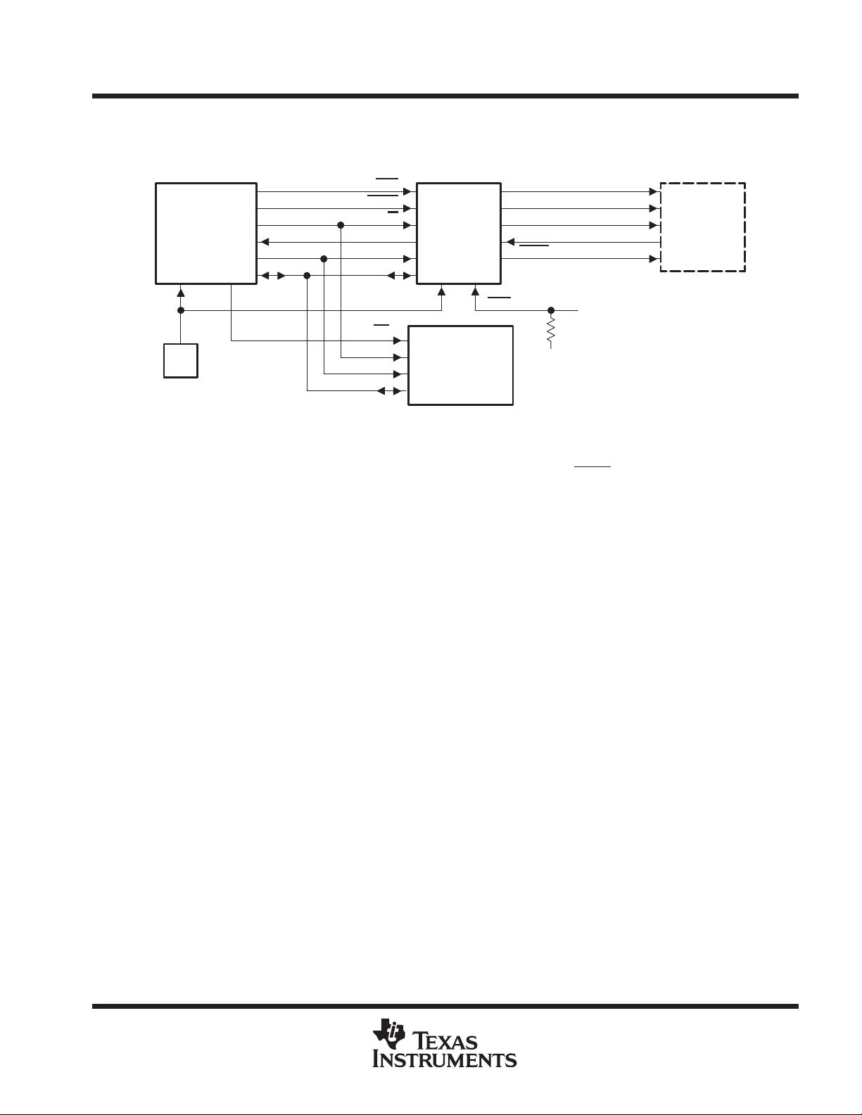
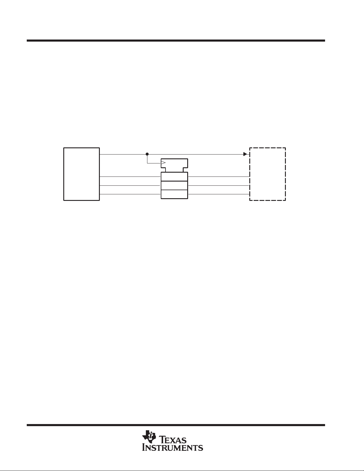
application information
In application, the eTBC is used to master a single IEEE Std 1149.1 TAP under the control of a
microprocessor/microcontroller host. A typical implementation is shown in Figure 1.
TCK
TMS
TDO
TDI
TRST
IEEE
Std 1149.1Compliant
Device Chain
(Target)
Microprocessor/
Microcontroller
(Host)
STRB
RDY
A (2–0)
D (7–0)
RST
R/W
’LVT8980
Embedded
Test
Bus
Controller
CLKIN TOE
CS
OSC
Program/Vector
Memory
(ROM/RAM)
(If/As Required)
GND
Figure 1. eTBC Application
All signals required to master IEEE Std 1149.1-compliant devices – TCK, TMS, TDO, TDI – are
sourced/received by the eTBC. The eTBC can also source the optional TRST signal. Additionally, the eTBC
implements high-drive output buffers, allowing it to interface directly to on- or off-board targets without need for
buffering or other additional logic.
The eTBC’s generic host interface allows it to act as a simple 8-bit memory- or I/O-mapped peripheral. As shown
in Figure 1, for many choices of host microprocessor/microcontroller, this interface can be accomplished without
additional logic. While the eTBC requires a clock input (CLKIN), in many cases it can be driven from the same
source that provides a clock signal to the host.
Thus, in combination with the host microprocessor/microcontroller, the eTBC can be used to implement a
two-chip embedded test-control function supporting board- and system-level built-in test based on structured
IEEE Std 1149.1 test access. In some cases, for additional program and/or test vector storage, an external
ROM/RAM may be required.
By use of the eTBC in such an embedded test control function, the host microprocessor/microcontroller is freed
from the burden of generating the T AP-state sequences, serializing the outgoing bit stream, and deserializing
the incoming bit stream. All such tasks are implemented in the eTBC, allowing the host to operate at full 8-bit
parallel efficiency, host software to operate at the level of discrete scan operations versus the level of TAP
manipulation, and test throughput to be maximized. The eTBC’s full suite of data-scan and instruction-scan
commands ensure that the host software operates efficiently.
Host efficiency and flexibility is also maximized through the eTBC’s fully visible status and implementation of
the ready output (RDY). RDY goes inactive during a read or write access if the host-requested access cannot
be performed immediately . Thus, it can be used to insert hold or wait states back to the host. When the condition
blocking the access clears, the requested access completes. Additionally, all conditions that can cause such
a blocking condition are continuously updated in the eTBC status and command registers. Thus, the host
software can poll the eTBC status rather than implement RDY in hardware.
POST OFFICE BOX 655303 • DALLAS, TEXAS 75265
5
Page 6
SN54LVT8980, SN74LVT8980
EMBEDDED TEST-BUS CONTROLLERS
IEEE STD 1149.1 (JTAG) TAP MASTERS WITH 8-BIT GENERIC HOST INTERFACES
SCBS676C – DECEMBER 1996 – REVISED AUGUST 1997
application information (continued)
The eTBC also provides several capabilities that support special target application requirements. The eTBC’s
test-output enable allows its master function to be disabled so that another device (an external tester, for
example) can control the target TAP. Where required, due to target non-compliance or sensitivity to state
sequencing, discrete-control mode provides the host software with arbitrary control of TMS and TDO
sequences. Also, where targets may be sensitive to leaving Shift-DR state during scan operation, gated-TCK
mode allows the TCK output to be stopped, rather than cycling the target T AP state to Pause-DR state, when
service to TDI buffer or TDO buffer is required.
Where target devices are extremely distant (due to cabling, etc.), pipelining may be implemented at intervals
along the incoming or outgoing paths to retime (deskew) the TDI, TDO, and TMS signals. An example is shown
in Figure 2. In such applications, the eTBC can automatically adjust the incoming test-data bit stream to account
for cycle delays introduced by the pipeline.
’LVT8980
eTBC
TCK
TMS
TDO
TDI
C1
1D
1D
1D
Distant
IEEE
Std
1149.1-
Compliant
Device
Chain
Figure 2. Retimed Interface to Target
Also, in gated-TCK mode, special scan commands provide transparent support for addressable shadow
protocols. Thus, in conjunction with its high-drive outputs, the eTBC can fully support multidrop backplane T AP
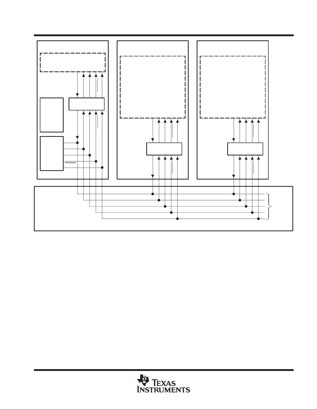
configurations implemented with TI’s addressable scan ports (ASP). Figure 3 shows a multidrop TAP
configuration in a passive-backplane application implemented with a centralized (one eTBC per chassis/rack)
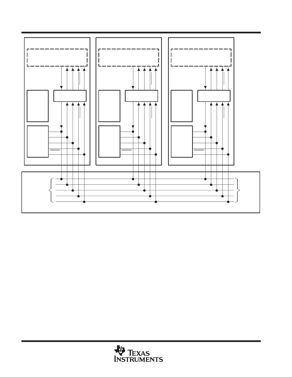
test-control architecture, while Figure 4 shows a passive-backplane application implemented with a distributed
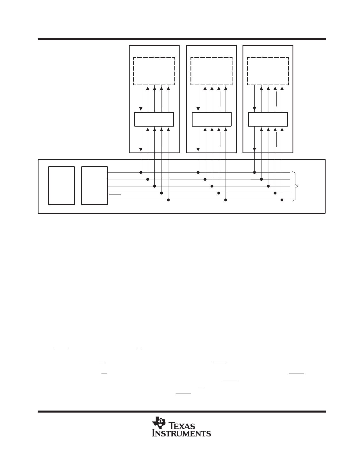
(eTBC per module) test-control architecture. Figure 5 shows a multidrop TAP configuration in an
active-backplane (motherboard) application.
6
POST OFFICE BOX 655303 • DALLAS, TEXAS 75265
Page 7
SN54LVT8980, SN74LVT8980
EMBEDDED TEST-BUS CONTROLLERS
IEEE STD 1149.1 (JTAG) TAP MASTERS WITH 8-BIT GENERIC HOST INTERFACES
SCBS676C – DECEMBER 1996 – REVISED AUGUST 1997
Plug-In Module
IEEE Std 1149.1-Compliant
Device Chain
STCK
STDI
ASP
(Host)
PTCK
Microcontroller
Microprocessor/
’LVT8980
etBC
PTDO
TDI
TCK
TMS
TDO
TRST
STDO
STMS
PTDI
PTMS
STRST
PTRST
Plug-In Module
IEEE Std 1149.1-Compliant
Device Chain
STDO
STMS
STCK
STDI
ASP
PTDI
PTCK
PTMS
PTDO
STRST
PTRST
Plug-In Module
IEEE Std 1149.1-Compliant
Device Chain
STDO
STMS
STCK
STDI
ASP
PTDI
PTCK
PTMS
PTDO
STRST
PTRST
To
Other
Modules
Passive Backplane
Figure 3. Passive-Backplane Application With Centralized (eTBC Per Chassis) Test-Control Architecture
POST OFFICE BOX 655303 • DALLAS, TEXAS 75265
7
Page 8
SN54LVT8980, SN74LVT8980
EMBEDDED TEST-BUS CONTROLLERS
IEEE STD 1149.1 (JTAG) TAP MASTERS WITH 8-BIT GENERIC HOST INTERFACES
SCBS676C – DECEMBER 1996 – REVISED AUGUST 1997
Plug-In Module
IEEE Std 1149.1-Compliant
Device Chain
STCK
STDI
ASP
(Host)
PTCK
Microcontroller
Microprocessor/
’LVT8980
etBC
PTDO
TDI
TCK
TMS
TDO
TRST
STDO
STMS
PTDI
PTMS
STRST
PTRST
Plug-In Module
IEEE Std 1149.1-Compliant
Device Chain
STCK
STDI
ASP
(Host)
PTCK
Microcontroller
Microprocessor/
’LVT8980
etBC
PTDO
TDI
TCK
TMS
TDO
TRST
STDO
STMS
PTDI
PTMS
STRST
PTRST
Plug-In Module
IEEE Std 1149.1-Compliant
Device Chain
STCK
STDI
ASP
(Host)
PTCK
Microcontroller
Microprocessor/
’LVT8980
etBC
PTDO
TDI
TCK
TMS
TDO
TRST
STDO
STMS
PTDI
PTMS
STRST
PTRST
To
Other
Modules
Passive Backplane
To
Other
Modules
Figure 4. Passive-Backplane Application With Distributed Test-Control (eTBC Per Card) Architecture
8
POST OFFICE BOX 655303 • DALLAS, TEXAS 75265
Page 9
SN54LVT8980, SN74LVT8980
EMBEDDED TEST-BUS CONTROLLERS
IEEE STD 1149.1 (JTAG) TAP MASTERS WITH 8-BIT GENERIC HOST INTERFACES
SCBS676C – DECEMBER 1996 – REVISED AUGUST 1997
’LVT8980
(Host)
Microcontroller
Microprocessor/
etBC
TDI
TCK
TMS
TDO
TRST
Plug-In Module
IEEE
Std
1149.1-Compliant
Device Chain
STRST
STDO
STMS
STCK
STDI
ASP
PTDI
PTCK
PTMS
PTDO
Active Backplane (Motherboard)
PTRST
Plug-In Module
IEEE
Std
1149.1-Compliant
Device Chain
STRST
STDO
STMS
STCK
STDI
ASP
PTDI
PTCK
PTMS
PTDO
PTRST
Plug-In Module
IEEE
Std
1149.1-Compliant
Device Chain
STRST
STDO
STMS
STCK
STDI
ASP
PTDI
PTCK
PTMS
PTDO
PTRST
To
Other
Modules
Figure 5. Active-Backplane (Motherboard) Application
architecture
Conceptually, the eTBC can be viewed as an IEEE Std 1149.1 coprocessor/accelerator that operates in
conjunction with (and under the control of) a host microprocessor/microcontroller. The eTBC implements this
function using an 8-bit generic host interface and a scan-test-based command/control architecture. As shown
in the functional block diagram, beyond these fundamental elements and another central block supporting
discrete-control mode, the eTBC functions are accomplished in four additional blocks – one for each of the
required TAP signals – a TCK generator, a TAP-state (TMS) generator, a TDO buffer, and a TDI buffer.
host interface
The eTBC host interface is implemented generically on an 8-bit read/write data bus (D7–D0). Three address
pins (A2–A0) directly index the eTBC’s eight read/write registers: configurationA, configurationB, status,
command, TDO buffer , TDI buffer, counter, and discrete control. The register address map is given in Table 1.
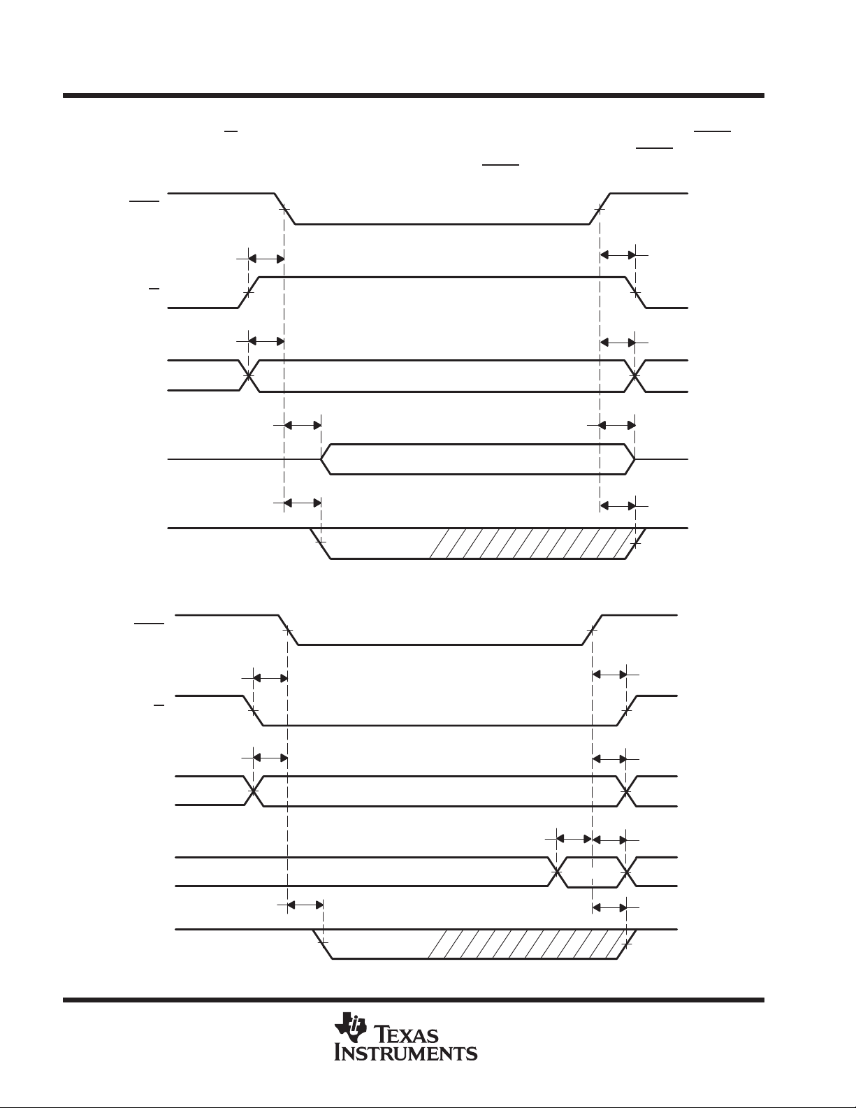
host access timing
Host access timing is asynchronous to the clock input (CLKIN) and is fully controlled by the read/write strobe
(STRB). The read/write select (R/W) serves to control the direction of data flow on the bidirectional data bus.
Figure 6 shows the read access timing while Figure 7 shows the write access timing. As shown, for either read
or write access, R/W
For read access (R/W high) the eTBC data bus outputs are made active, on the falling edge of STRB, to drive
the data contained in the selected eTBC register. Otherwise, when STRB is high, the eTBC data outputs are
at high impedance. Therefore, in many applications, the R/W signal can be shared in common with other host
peripherals (ROM or RAM, for example) while the STRB signal is generated separately (by discrete chip-select
signals available from the host or a decode logic) for each required peripheral.
and address signals should be held while STRB is low.
POST OFFICE BOX 655303 • DALLAS, TEXAS 75265
9
Page 10
SN54LVT8980, SN74LVT8980
EMBEDDED TEST-BUS CONTROLLERS
IEEE STD 1149.1 (JTAG) TAP MASTERS WITH 8-BIT GENERIC HOST INTERFACES
SCBS676C – DECEMBER 1996 – REVISED AUGUST 1997
host access timing (continued)
For write access (R/W low), the eTBC data outputs remain at high impedance independent of STRB. The
address of the register to be written is latched from the address pins on the falling edge of STRB, while the data
to be written is latched from the data bus on the rising edge of STRB.
STRB
t
h
R/W
t
su
A
D
RDY
STRB
R/W
t
PZH
t
su
Valid
or t
PZL
t
PHL
t
PHZ
or t
PLZ
t
h
t
PLH
Figure 6. Read Access Timing
t
t
su
h
10
RDY
t
su
A
D
t
PHL
Valid
t
su
Valid
t
h
t
h
t
PLH
Figure 7. Write Access Timing
POST OFFICE BOX 655303 • DALLAS, TEXAS 75265
Page 11

SN54LVT8980, SN74LVT8980
EMBEDDED TEST-BUS CONTROLLERS
IEEE STD 1149.1 (JTAG) TAP MASTERS WITH 8-BIT GENERIC HOST INTERFACES
SCBS676C – DECEMBER 1996 – REVISED AUGUST 1997
ready output
The ready output (RDY) from the host interface can be used, where the selected microprocessor/microcontroller
supports it, to insert wait or hold states back to the host. If a host-requested access cannot be performed
immediately , RDY goes inactive (low) during that given access. When the condition blocking the access clears,
RDY goes active (high) and the eTBC grants the requested access. Alternatively, where such
hardware-generated hold or wait states are not supported in the selected microprocessor/microcontroller host,
the eTBC status and/or command registers can be polled to determine its readiness to grant a given read or
write access.
Conditions that cause a host access to be blocked (and RDY to become inactive) are limited to the following:
D
While the TDI buffer is empty, as indicated in status register (bit 7, TDIS), a requested read to TDI-buffer
register generates RDY inactive; this condition clears, RDY goes active, and the requested access
completes, when the TDI buffer is no longer empty.
D
While the TDO buffer is full or is being reset upon initiation of a scan command, as indicated in status register
(bit 6, TDOS), a requested write to TDO-buffer register generates RDY inactive; this condition clears, RDY
goes active, and the requested access completes, when the TDO buffer is no longer full or the TDO-buffer
reset completes, as applicable.
D
While a command is in progress, as indicated by a non-zero value in the opcode field (bits 3–0, OPCOD)
of the command register, a requested write to command, configurationA, configurationB, or counter
registers generates RDY inactive. This condition clears, RDY goes active, and the requested access is
complete, when the previously specified command finishes. The sole exception is the writing of a logic 1
into the software reset (bit 7, SWRST) bit of the command register, which is never blocked.
D
While a full-duplex scan command is in progress, and the number of retiming-delay bits is other than zero,
the number of writes to TDO-buffer register may not exceed, by more than 5, the number of reads to
TDI-buffer register . A write to TDO-buffer register that does exceed this limit is blocked, and generates RDY
inactive, indefinitely; the TDI-buffer register must be read before another write to TDO-buffer register.
POST OFFICE BOX 655303 • DALLAS, TEXAS 75265
11
Page 12

SN54LVT8980, SN74LVT8980
REGISTER
BIT 6
BIT 5
BIT 4
BIT 3
BIT 2
BIT 1
EMBEDDED TEST-BUS CONTROLLERS
IEEE STD 1149.1 (JTAG) TAP MASTERS WITH 8-BIT GENERIC HOST INTERFACES
SCBS676C – DECEMBER 1996 – REVISED AUGUST 1997
register descriptions
A summary of the eTBC registers, their address mappings, bit assignments, reset values, and host accessibility
(read/write or read-only) is provided in T able 1. All registers are fully readable by the host. All registers are fully
writeable by the host with the exception of the status and TDI-buffer registers. Also, with the exception of
TDO-buffer and command registers, writes to any register while a command is in progress are held off (RDY
inactive) or ignored. Bits designated as reserved should be written to logic 0; read-only bits designated as
reserved always read logic 0.
T able 1. Register Summary
REGISTER DETAIL
ADDRESS
A2–A0
000 ConfigurationA Reserved NTOE LPBK MODE 0x00 R/W
001 ConfigurationB CDIV Reserved RDLY 0x80 R/W
010 Status TDIS TDOS CTRS Reserved TAPST 0x00 R
011 Command SWRST NTRST ENDST OPCOD 0x00 R/W
100 TDO buf fer 0x00 R/W
101 TDI buffer 0x00 R
110 Counter 0x00 R/W
111 Discrete control Reserved DNTR DTMS DTDI DTDO 0x00 R/W
BIT 7
(MSB)
(BIT ASSIGNMENTS)
BIT 0
(LSB)
RESET HOST
VALUE ACCESS
configuration registers
All eTBC test commands operate under the influence of the configurationA and configurationB registers. The
decodes of the various bit groups assigned to these registers are given in Table 2 and Table 3, respectively.
These registers are fully readable at all times and are fully writeable except when an eTBC command is in
progress. Bit group values designated as reserved should not be written.
12
POST OFFICE BOX 655303 • DALLAS, TEXAS 75265
Page 13

NTOE
5
LPBK
4–3
IEEE STD 1149.1 (JTAG) TAP MASTERS WITH 8-BIT GENERIC HOST INTERFACES
CONFIGURATIONA
BIT
GROUP
MODE 2–0
BIT NO.
SN54LVT8980, SN74LVT8980
EMBEDDED TEST-BUS CONTROLLERS
SCBS676C – DECEMBER 1996 – REVISED AUGUST 1997
Table 2. ConfigurationA Register Decode
VALUE RESULT
0 TAP outputs (TCK, TDO, TMS, TRST) are enabled.
1 TAP outputs (TCK, TDO, TMS, TRST) are disabled (high impedance).
00 No loopback – TDI pin inputs to TDI buffer.
01 TMS loopback – TAP-state generator inputs to TDI buffer. TMS and TDO pins are fixed high.
10 TDO loopback – TDO buffer inputs to TDI buffer. TMS and TDO pins are fixed high.
11 Reserved
Automatic/free-running-TCK mode – all TAP outputs are generated autonomously in the eTBC according
000
001
010
011–111 Reserved
to the active command. The TCK output runs continuously; while operating a scan command, if the TDI
buffer becomes full and/or the TDO buffer becomes empty, the TAP state is cycled to Pause-DR or
Pause-IR, as appropriate, until the host performs the required buffer service.
Automatic/gated-TCK mode – all T AP outputs are generated autonomously in the eTBC according to the
active command. The TCK output is run only when required to move TAP state or to progress run-test or
scan operations, otherwise, it is gated off (low); while operating a scan command, if the TDI buffer
becomes full and/or the TDO buffer becomes empty, the TAP state remains in Shift-IR or Shift-DR, as
appropriate, but the TCK output is gated off until the host performs the required buffer service.
Discrete-control mode – all TAP outputs are determined by contents of the discrete-control register under
control of host software.
Table 3. ConfigurationB Register Decode
CONFIGURATIONB
BIT
GROUP
CDIV 7–5 000–111 TCK = (CLKIN)/(2
RDLY 3–0
BIT NO.
VALUE RESULT
CDIV
); reset value TCK = (CLKIN)/(24) = CLKIN/16
0000–1 1
11
Number of retiming delays to accommodate = RDL Y; while operating a scan command, TDI sampling is
delayed by a number of TCK cycles, equal to RDLY , following the generation of Shift-DR or Shift-IR state,
as appropriate.
The negated test-output-enable (NTOE) bit allows the host to disable the T AP outputs via software in a manner
analogous to the hardware TOE. The loopback (LPBK) bit group allows the selection of the source of data to
be input to the TDI buffer – from the TDI pin for normal eTBC operations or , for eTBC verification purpose, from
TAP-state (TMS) generator or TDO buffer. The test mode (MODE) bit group provides a choice of
automatic/free-running-TCK, automatic/gated-TCK, or discrete-control modes.
The clock-divisor (CDIV) bit group allows software control of the TCK output frequency based on a division of
the CLKIN input. Divisors from 20 (1) to 27 (128) are provided. The clock divisor defaults to 24 (16) on eTBC
reset (power-up, hardware-initiated, or software-initiated). The retiming-delay (RDL Y) bit group provides for the
automatic accommodation of retiming (pipeline) delays, which can be used to deskew the T AP signals to target
scan chains that are electrically distant (due to cabling delays, etc).
POST OFFICE BOX 655303 • DALLAS, TEXAS 75265
13
Page 14

SN54LVT8980, SN74LVT8980
TDIS
7
TDOS
6
TAPST
3–0
EMBEDDED TEST-BUS CONTROLLERS
IEEE STD 1149.1 (JTAG) TAP MASTERS WITH 8-BIT GENERIC HOST INTERFACES
SCBS676C – DECEMBER 1996 – REVISED AUGUST 1997
status register
The status of the eTBC is fully reported and continuously updated in the status register. The decode of the
various bit groups assigned to the status register is given in Table 4.
Table 4. Status Register Decode
STATUS
BIT
GROUP
CTRS 5
BIT NO.
VALUE RESULT
0 The TDI buffer is empty – no TDI data is available for host read.
1 The TDI buffer is not empty – at least one byte of TDI data is available for host read.
0 The TDO buffer is not full – at least one byte in TDO buffer is available for host write.
1 The TDO buffer is full – no bytes in TDO buffer are available for host write.
The counter is not loaded with a complete 32-bit value – command operation cannot begin until counter
0
load completes.
1 The counter is loaded with a complete 32-bit value – command operation can begin.
0000 The current target TAP state (as sent by eTBC) is Test-Logic-Reset.
0001 The current target TAP state (as sent by eTBC) is Select-DR-Scan.
0010 The current target TAP state (as sent by eTBC) is Capture-DR.
0011 The current target TAP state (as sent by eTBC) is Shift-DR.
0100 The current target TAP state (as sent by eTBC) is Exit1-DR.
0101 The current target TAP state (as sent by eTBC) is Pause-DR.
0110 The current target TAP state (as sent by eTBC) is Exit2-DR.
0111 The current target TAP state (as sent by eTBC) is Update-DR.
1000 The current target TAP state (as sent by eTBC) is Run-Test/Idle.
1001 The current target TAP state (as sent by eTBC) is Select-IR-Scan.
1010 The current target TAP state (as sent by eTBC) is Capture-IR.
1011 The current target TAP state (as sent by eTBC) is Shift-IR
1100 The current target TAP state (as sent by eTBC) is Exit1-IR.
1101 The current target TAP state (as sent by eTBC) is Pause-IR.
1110 The current target TAP state (as sent by eTBC) is Exit2-IR.
1111 The current target TAP state (as sent by eTBC) is Update-IR.
The TDI-buffer-status (TDIS) bit reports the readiness of the TDI buffer to respond to a host read. The
TDO-buffer-status (TDOS) bit reports the readiness of the TDO buffer to respond to a host write. The
counter-status (CTRS) bit reports the readiness of the counter to support a command that uses the counter. The
current-TAP-state (TAPST) bit group continuously reports the target TAP state as monitored by the eTBC.
command register
The command register is used to perform software reset of the eTBC, to discretely control the state of the TRST
output when not in discrete-control mode, and to initiate test operations in the target(s).The decode of the
various bits assigned to the command register is given in Table 5.
Any read to the command register while a command is in progress returns the value written to the command
register upon initiation of the command. Once a command finishes, the operation-code (OPCOD) bit group in
the command register is reset to null. In this way , the status of a requested command can be monitored/polled
by the host.
With the exception of the software-reset (SWRST) bit, which can be written at any time, writes to the command
register while a command is in progress causes RDY inactive and is ignored if the write cycle is terminated
before the previously requested command finishes.
14
POST OFFICE BOX 655303 • DALLAS, TEXAS 75265
Page 15

SWRST
7
TRST
6
ENDST
5–4
OPCOD
3–0
SN54LVT8980, SN74LVT8980
EMBEDDED TEST-BUS CONTROLLERS
IEEE STD 1149.1 (JTAG) TAP MASTERS WITH 8-BIT GENERIC HOST INTERFACES
SCBS676C – DECEMBER 1996 – REVISED AUGUST 1997
Table 5. Command Register Decode
COMMAND TEST OPERATION COMMENTS
BIT
GROUP
VALUE RESULT
BIT
NO.
0 Normal operation
1 Full reset
0 If not in discrete-control mode, output high to TRST pin
1 If not in discrete-control mode, output low to TRST pin
00 Finish command in TAP state Test-Logic-Reset
01 Finish command in TAP state Run-Test/Idle
10 Finish command in TAP state Pause-DR
11 Finish command in TAP state Pause-IR
0000 Null
0001 Reserved
0010 Execute run test Run-Test/Idle Yes No No
0011 Execute input-only ASP scan N/A Yes Yes No
0100 Execute ASP scan N/A Yes Yes Yes
0101 Execute output-only ASP scan N/A Yes No Yes
0110 Execute state move N/A No No No
0111 Execute state jump N/A No No No
1000 Execute instruction-register scan Shift-IR Yes Yes Yes
1001 Execute data-register scan Shift-DR Yes Yes Yes
1010 Execute input-only instruction-register scan Shift-IR Yes Yes No
1011 Execute input-only data-register scan Shift-DR Yes Yes No
1100 Execute output-only instruction-register scan Shift-IR Yes No Yes
1101 Execute output-only data-register scan Shift-DR Yes No Yes
1110 Execute recirculate instruction-register scan Shift-IR Yes Yes No
1111 Execute recirculate data-register scan Shift-DR Yes Yes No
WORKING
TAP STATE
USES
COUNTER
USES
BUFFER
TDI
USES
TDO
BUFFER
The software-reset (SWRST) bit is provided to allow software initiation of full eTBC reset. This bit of the
command register can be written at any time, regardless of the configuration or command in progress. The
test-reset (TRST) bit allows direct software control of the state of TRST
output in modes other than
discrete control.
The end-T AP-state (ENDST) bit group determines the T AP state in which the target scan chain is left when the
requested command finishes. The operation-code (OPCOD) bit group determines the test operation to be
executed in the target.
POST OFFICE BOX 655303 • DALLAS, TEXAS 75265
15
Page 16

SN54LVT8980, SN74LVT8980
VALUE
RESULT
DNTR
3
DTMS
2
DTDI
1
DTDO
0
EMBEDDED TEST-BUS CONTROLLERS
IEEE STD 1149.1 (JTAG) TAP MASTERS WITH 8-BIT GENERIC HOST INTERFACES
SCBS676C – DECEMBER 1996 – REVISED AUGUST 1997
counter register
The counter register, while only 8 bits wide like any other eTBC register, provides read/write access to the full
32-bit eTBC counter. Writes to the counter register are accomplished by four complete host access cycles,
otherwise the counter is considered unloaded (CTRS = 0). Reads to the counter register likewise are
accomplished by four complete host access cycles. However, reads do not affect the counter-loaded status
(CTRS). The counter access (both read and write) is in least-significant-byte-first order. Any writes to the counter
register while a command is in progress are ignored. The 32-bit value present in the counter at initiation of a
command is used to determine the number of TCK cycles or scan bits for which the command is operated.
TDO-buffer register
The TDO-buffer register, while only 8 bits wide like any other eTBC register, provides write access to the full
4 × 8 (32-bit) FIFO that comprises the TDO buffer. The TDO-buf fer register can be written as long as the TDO
buffer does not become full. When the TDO buffer becomes full, further writes to the TDO-buffer register cause
RDY inactive (and consequent hold or wait states to be sent back to the host, if supported) and cause the write
to be ignored if the write cycle is terminated before the TDO-buffer-full status is cleared.
TDI-buffer register
The TDI-buffer register , while only 8 bits wide like any other eTBC register, provides read access to the full 4 × 8
(32-bit) FIFO that comprises the TDI buffer . The TDI-buffer register can be read as long as the TDI buffer does
not become empty. When the TDI buffer becomes empty, further reads to the TDI-buffer register cause RDY
inactive (and consequent hold or wait states to be sent back to the host, if supported) and cause the read data
to be invalid if the read cycle is terminated before the TDI-buffer-empty status is cleared.
discrete-control register
The discrete-control register is used to program the state of the T AP outputs (TCK, TDO, TMS, TRST
poll the state of the TAP input (TDI) when the eTBC is in its discrete-control mode. The contents of the
discrete-control register determine values output to TDO, TMS, and TRST according to the decode in Table 6.
The TCK output is generated on each read and write to the discrete-control register; writes generate TCK falling
edge, while reads generate TCK rising edge. In modes other than the discrete-control mode, this register is fully
writeable and readable, but writes and reads have no effect on eTBC or target operation.
Table 6. Discrete-Control Register Decode
DISCRETE CONTROL
BIT GROUP BIT NO.
0 If in discrete-control mode, output low to TRST pin, otherwise nothing
1 If in discrete-control mode, output high to TRST pin, otherwise nothing
0 If in discrete-control mode, output low to TMS pin, otherwise nothing
1 If in discrete-control mode, output high to TMS pin, otherwise nothing
0 The TDI data received is a logic 0.
1 The TDI data received is a logic 1.
0 If in discrete-control mode, output low to TDO pin, otherwise nothing
1 If in discrete-control mode, output high to TDO pin, otherwise nothing
) and to
16
POST OFFICE BOX 655303 • DALLAS, TEXAS 75265
Page 17

SN54LVT8980, SN74LVT8980
EMBEDDED TEST-BUS CONTROLLERS
IEEE STD 1149.1 (JTAG) TAP MASTERS WITH 8-BIT GENERIC HOST INTERFACES
SCBS676C – DECEMBER 1996 – REVISED AUGUST 1997
command/control
The eTBC’s command-based architecture is structured around a set of comprehensive IEEE Std 1 149.1 (JTAG)
test objectives, which include TAP state movement, scan operations, and run test (operation of test logic in
Run-Test/Idle state). The set of test operations, as decoded from the command register (bits 3–0, OPCOD) is
given in T able 5. Commands are initiated by writing the eTBC command register; upon command initiation, the
test-control logic is initialized and the TDO and TDI buffers are cleared. Command completion is indicated when
the operation code (OPCOD) field of the command register returns to the value of the null command.
The eTBC command operation is modified by the configurationA, and configurationB registers, which should
be written prior to writing the command register, as the values in these registers cannot be modified while a
command is in progress. Also, commands are only operated in automatic test modes, as specified in the
configurationA register (bits 2–0, MODE) – while in the discrete-control mode, commands are ignored.
All eTBC commands operate similarly to accomplish IEEE Std 1 149.1 test objectives. First, the eTBC generates
a TMS sequence to move the target scan chain from its current T AP state to a working state that depends on
the test objective. Second, the command is operated (test run, bits scanned) in the working state for a number
of TCK cycles (or scan bits) determined by the value of the counter upon command initiation. Third, the eTBC
generates a TMS sequence to move the target scan chain from the working state to the end state specified in
the command register (bits 5–4, ENDST). For some commands, one or more of these steps are omitted.
T AP-state-movement commands
Two eTBC commands are provided to accomplish TAP state movement. The state-move command operates
to generate a TMS sequence to move the target scan chain directly from its current T AP state to the end state
specified in the command register. The state-jump command moves the eTBC’ s stored value of the target T AP
state without generating any changes to the TMS output. The state-jump command can therefore be used to
switch between targets that share the same test bus, such as those in a multidrop backplane configuration
implemented with TI addressable scan ports, but that may be left in different TAP states.
run-test command
The run-test command allows the test logic of the target scan chain to execute autonomously in the
Run-Test/Idle TAP state. Such test logic is commonly used to implement chip- or board-level built-in self test.
The run-test command generates TMS sequences to move the target scan chain from its current T AP state to
the Run-T est/Idle T AP state where it remains for a number of TCK cycles determined by the value of the counter
upon command initiation. Upon the countdown of the counter to zero, the eTBC generates TMS sequences to
move the target scan chain to the end state specified in the command register.
scan commands
Eleven eTBC commands are provided to perform scan operations to target scan chains. These can be classified
by the destination of scan data in the target – addressable scan port (ASP), IEEE Std 1 149.1 instruction register,
or IEEE Std 1149.1 data register – and by the nature/direction of the data transfer – full-duplex (default),
input-only, output-only, or recirculate. The only combination of these two factors that is not implemented is
recirculate ASP scan.
addressable scan port (ASP) scan commands
The ASP scan commands scan data to and/or from an addressable scan port target. Since ASP devices require
that TMS remain fixed throughout their select and acknowledge protocols, the eTBC does not generate TMS
sequences or change its stored value of the target’s T AP state. Also, for the same reason, ASP scan commands
that target ASP devices should be operated in gated-TCK mode. The ASP scan commands do allow data written
to the TDO buffer to be driven serially onto the TDO pin and bits received serially at the TDI pin to be stored
into the TDI buffer for reading by the host. However, the ASP scan commands do not perform any bit-pair
encoding of ASP select protocols or decoding of ASP acknowledge protocols. Such encoding/decoding must
be performed in the host. The number of data bits transferred in and/or out is determined by the value of the
counter upon command initiation.
POST OFFICE BOX 655303 • DALLAS, TEXAS 75265
17
Page 18

SN54LVT8980, SN74LVT8980
EMBEDDED TEST-BUS CONTROLLERS
IEEE STD 1149.1 (JTAG) TAP MASTERS WITH 8-BIT GENERIC HOST INTERFACES
SCBS676C – DECEMBER 1996 – REVISED AUGUST 1997
instruction-register scan commands
The instruction-register scan commands scan bits to and/or from the concatenation of instruction registers in
a target scan chain. The eTBC generates a TMS sequence to move the target scan chain from its current T AP
state to the Shift-IR T AP state. Data written to the TDO buffer can be driven serially onto the TDO pin and bits
received serially at the TDI pin can be stored into the TDI buffer for reading by the host. The number of data
bits transferred in and/or out is determined by the value of the counter upon command initiation. If, during the
operation of an instruction register scan command, the TDO buffer becomes empty , or the TDI buffer becomes
full, the T AP state is sequenced to Pause-IR (if in free-running-TCK mode) or the TCK output is gated off (if in
gated-TCK mode) until the required buffer service is performed. Upon the countdown of the counter to zero,
the eTBC generates TMS sequences to move the target scan chain to the end state specified in the command
register.
data-register scan commands
The data-register scan commands operate to scan bits to and/or from the concatenation of data registers in a
target scan chain. The eTBC generates a TMS sequence to move the target scan chain from its current TAP
state to the Shift-DR T AP state. Data written to the TDO buffer may be driven serially onto the TDO pin and bits
received serially at the TDI pin may be stored into the TDI buffer for reading by the host. The number of data
bits transferred in and/or out is determined by the value of the counter upon command initiation. If, during the
operation of a data-register scan command, the TDO buffer becomes empty , or the TDI buffer becomes full, the
TAP state is sequenced to Pause-DR (if in free-running-TCK mode) or the TCK output is gated off (if in
gated-TCK mode) until the required buffer service is performed. Upon the countdown of the counter to zero,
the eTBC generates TMS sequences to move the target scan chain to the end state specified in the
command register.
other scan-command variations
As noted before, the nature/direction of the data transfer for any scan command can vary along with the
destination of scan data in the target, as follows:
D
For scan commands of the full-duplex (default) class, both TDO buffer and TDI buffer are used to scan data
to and from the target scan chain, respectively.
D
For scan commands of the input-only class, only the TDI buffer is used to scan data from the target scan
chain; outgoing TDO data is fixed at a high level throughout the scan operation.
D
For scan commands of the output-only class, only the TDO buffer is used to scan data to the target scan
chain; incoming TDI data is simply ignored.
D
For scan commands of the recirculate class, only the TDI buffer is used to scan data from the target scan
chain; outgoing TDO data is generated by recirculating the incoming TDI data back into the target
scan chain.
counter
As described above, the value loaded in the eTBC’s 32-bit counter at initiation of a command is used to specify
the number of TCK cycles or scan bits to remain in the command’s working state. As each TCK cycle or scan
bit is processed for a run-test or scan command, respectively, the counter value is decremented. When the
counter value reaches zero, the command leaves its working state to finish in the end state specified in the
command register.
Before a command that uses the counter can be initiated, a full 32-bit value should be loaded by four consecutive
writes to the counter register. As well, the full 32-bit current value of the counter can be observed by four
consecutive reads to the counter register. The counter status (unloaded/loaded) is maintained and observable
in the status register (bit 5, CTRS).
Upon eTBC reset (power-up, hardware-initiated, or software-initiated), the counter is cleared and assumes its
unloaded state.
18
POST OFFICE BOX 655303 • DALLAS, TEXAS 75265
Page 19

SN54LVT8980, SN74LVT8980
EMBEDDED TEST-BUS CONTROLLERS
IEEE STD 1149.1 (JTAG) TAP MASTERS WITH 8-BIT GENERIC HOST INTERFACES
SCBS676C – DECEMBER 1996 – REVISED AUGUST 1997
TCK generator
The TCK generator sources the test clock (TCK) signal required by the IEEE Std 1149.1 target(s) and the
eTBC-internal test-control logic. The fundamental TCK frequency is produced by division of CLKIN. The divisor
is programmable within a range of 1 to 128 in the configurationB register (bits 7–5, CDIV). The TCK output to
the target(s) operate in free-running or gated modes. The free-running mode toggles TCK continuously , based
on CLKIN, while the gated mode operates the TCK only when required to move the target T AP state or to perform
a run-test or scan operation.
While the eTBC is in discrete-control mode, the TCK generator is not used; instead, the state of TCK is toggled
on each alternating read and write to the discrete-control register. A falling edge of TCK is produced by write,
while a rising edge of TCK is produced by read.
Upon eTBC reset (power-up, hardware-initiated, or software-initiated), the TCK generator assumes its
free-running mode with a clock divisor of 16 (TCK = CLKIN/16).
TAP-state generator
The TAP-state generator sources the TMS signal, which sequences the TAP controllers of connected
IEEE Std 1149.1-compliant target devices. The TAP controller specified by IEEE Std 1149.1 is a synchronous
finite-state machine that provides test control signals throughout each target device; its state diagram is shown
in Figure 8. This diagram and the TAP-controller states are discussed subsequently.
The T AP-state generator operates under the control of an executing command to generate the TMS sequences
required to move connected target devices from one stable state to another, to capture and scan test data
into/out of target devices, and to operate built-in test modes of target devices in the Run-Test/Idle state.
The TAP state currently being generated is always maintained by the TAP-state generator and is constantly
available in the eTBC status register (bits 3–0, T APST) for host read. Based on the TAP state that is current upon
command initiation, the TAP-state generator will source a defined sequence of TMS values to reach the T AP
state in which the command is progressed (e.g., Shift-IR, Shift-DR, Run-Test/Idle), and ultimately to reach the
specified end TAP state. These sequences are detailed in Tables 7–12.
While the eTBC is in free-running-TCK mode, if a currently operating scan command empties or fills a required
test data buffer, then the TAP-state generator sources the TMS sequences required to move the connected
target devices to their Pause-IR or Pause-DR states. In such case, the TAP-state generator maintains target
devices in their Pause-IR or Pause-DR states until the required test data buffer is serviced appropriately.
However, if such a buffer condition occurs while the eTBC is in gated-TCK mode, the TAP-state generator
maintains the target devices in their Shift-IR or Shift-DR states while the TCK is gated off.
While the eTBC is in discrete-control mode, the T AP-state generator is not used; instead, the state of the TMS
pin is determined by the contents of the discrete-control register. Thus, TMS sequences that cannot be
generated automatically still can be applied through the eTBC to targets that require such (e.g., near-compliant
devices).
The TAP-state generator also is not used during the operation of the special addressable shadow protocol
(ASP) scan commands. Since, by definition, ASPs operate only while the T AP is idling (maintaining one of the
T AP states Test-Logic-Reset, Run-Test/Idle, Pause-IR, or Pause-DR), the TMS pin must be maintained at the
value it held upon initiation of the ASP scan command.
For eTBC verification/debugging, in addition to continuous update of the current target T AP state in the eTBC
status register, the output of the TAP-state (TMS) generator can be selected for loopback into the TDI buffer.
When this TMS-loopback mode is selected, although a host-requested command executes in the eTBC, the
target is not affected, as both TMS and TDI are fixed at a high level.
Upon eTBC reset (power up, hardware initiated, or software initiated), the TAP-state generator assumes the
Test-Logic-Reset TAP state.
POST OFFICE BOX 655303 • DALLAS, TEXAS 75265
19
Page 20

SN54LVT8980, SN74LVT8980
EMBEDDED TEST-BUS CONTROLLERS
IEEE STD 1149.1 (JTAG) TAP MASTERS WITH 8-BIT GENERIC HOST INTERFACES
SCBS676C – DECEMBER 1996 – REVISED AUGUST 1997
Table 7. TMS Sequencing From TAP State Test-Logic-Reset
FROM TEST-LOGIC-RESET (TMS = H) TO:
TEST-LOGIC-RESET RUN-TEST-IDLE SHIFT-DR PAUSE-DR SHIFT-IR PAUSE-IR
NEXT
TMS
H T-L-R L R-T/I L R-T/I L R-T/I L R-T/I L R-T/I
TEST-LOGIC-RESET RUN-TEST-IDLE SHIFT-DR PAUSE-DR SHIFT-IR PAUSE-IR
NEXT
TMS
H S-DR-S L R-T/I H S-DR-S H S-DR-S H S-DR-S H S-DR-S
H S-IR-S L Capture-DR L Capture-DR H S-IR-S H S-IR-S
H T-L-R L Shift-DR H Exit1-DR L Capture-IR L Capture-IR
NEXT
TAP
STATE
NEXT
TAP
STATE
NEXT
TMS
NEXT
TMS
NEXT
TAP
STATE
NEXT
TMS
H S-DR-S H S-DR-S H S-DR-S H S-DR-S
L Capture-DR L Capture-DR H S-IR-S H S-IR-S
L Shift-DR H Exit1-DR L Capture-IR L Capture-IR
NEXT
TAP
STATE
NEXT
TMS
L Pause-DR L Shift-IR H Exit1-IR
NEXT
TAP
STATE
NEXT
TMS
Table 8. TMS Sequencing From TAP State Run-Test/Idle
FROM RUN-TEST/IDLE (TMS = L) TO:
NEXT
TAP
STATE
NEXT
TMS
NEXT
TAP
STATE
NEXT
TMS
L Pause-DR L Shift-IR H Exit1-IR
NEXT
TAP
STATE
NEXT
TMS
NEXT
TAP
STATE
NEXT
TAP
STATE
NEXT
TMS
L Pause-IR
NEXT
TMS
L Pause-IR
NEXT
TAP
STATE
NEXT
TAP
STATE
Table 9. TMS Sequencing From TAP State Pause-DR
FROM PAUSE-DR (TMS = L) TO:
TEST-LOGIC-RESET RUN-TEST-IDLE SHIFT-DR PAUSE-DR SHIFT-IR PAUSE-IR
NEXT
TMS
H Exit2-DR H Exit2-DR H Exit2-DR H Exit2-DR H Exit2-DR H Exit2-DR
H Update-DR H Update-DR L Shift-DR H Update-DR H Update-DR H Update-DR
H S-DR-S L R-T/I H S-DR-S H S-DR-S H S-DR-S
H S-IR-S L Capture-DR H S-IR-S H S-IR-S
H T-L-R H Exit1-DR L Capture-IR L Capture-IR
NEXT
TAP
STATE
NEXT
TMS
NEXT
TAP
STATE
NEXT
TMS
NEXT
TAP
STATE
NEXT
TMS
L Pause-DR L Shift-IR H Exit1-IR
NEXT
TAP
STATE
NEXT
TMS
NEXT
TAP
STATE
NEXT
TMS
L Pause-IR
STATE
NEXT
TAP
20
POST OFFICE BOX 655303 • DALLAS, TEXAS 75265
Page 21

SN54LVT8980, SN74LVT8980
EMBEDDED TEST-BUS CONTROLLERS
IEEE STD 1149.1 (JTAG) TAP MASTERS WITH 8-BIT GENERIC HOST INTERFACES
SCBS676C – DECEMBER 1996 – REVISED AUGUST 1997
Table 10. TMS Sequencing From TAP State Pause-IR
FROM PAUSE-IR (TMS = L) TO:
TEST-LOGIC-RESET RUN-TEST-IDLE SHIFT-DR PAUSE-DR SHIFT-IR PAUSE-IR
NEXT
TMS
H Exit2-IR H Exit2-IR H Exit2-IR H Exit2-IR H Exit2-IR H Exit2-IR
H Update-IR H Update-IR H Update-IR H Update-IR L Shift-IR H Update-IR
H S-DR-S L R-T/I H S-DR-S H S-DR-S H S-DR-S
H S-IR-S L Capture-DR L Capture-DR H S-IR-S
H T-L-R L Shift-DR H Exit1-DR L Capture-IR
NEXT TMS NEXT TAP STATE NEXT TMS NEXT TAP STATE NEXT TMS NEXT TAP STATE NEXT TMS NEXT TAP STATE
NEXT
TAP
STATE
TEST-LOGIC-RESET RUN-TEST-IDLE PAUSE-DR PAUSE-IR
H Exit1-DR H Exit1-DR H Exit1-DR H Exit1-DR
H Update-DR H Update-DR L Pause-DR H Update-DR
H S-DR-S L R-T/I H S-DR-S
H S-IR-S H S-IR-S
H T-L-R L Capture-IR
NEXT
TMS
NEXT
TAP
STATE
NEXT
TMS
NEXT
TAP
STATE
NEXT
TMS
L Pause-DR H Exit1-IR
NEXT
TAP
STATE
NEXT
TMS
Table 11. TMS Sequencing From TAP State Shift-DR
FROM SHIFT-DR (TMS = L) TO:
NEXT
TAP
STATE
NEXT
TMS
L Pause-IR
H Exit1-IR
L Pause-IR
NEXT
TAP
STATE
Table 12. TMS Sequencing From TAP State Shift-IR
FROM SHIFT-IR (TMS = L) TO:
TEST-LOGIC-RESET RUN-TEST-IDLE PAUSE-DR PAUSE-IR
NEXT TMS NEXT TAP STATE NEXT TMS NEXT TAP STATE NEXT TMS NEXT TAP STATE NEXT TMS NEXT TAP STATE
H Exit1-IR H Exit1-IR H Exit1-IR H Exit1-IR
H Update-IR H Update-IR H Update-IR L Pause-IR
H S-DR-S L R-T/I H S-DR-S
H S-IR-S L Capture-DR
H T-L-R H Exit1-DR
L Pause-DR
POST OFFICE BOX 655303 • DALLAS, TEXAS 75265
21
Page 22

SN54LVT8980, SN74LVT8980
EMBEDDED TEST-BUS CONTROLLERS
IEEE STD 1149.1 (JTAG) TAP MASTERS WITH 8-BIT GENERIC HOST INTERFACES
SCBS676C – DECEMBER 1996 – REVISED AUGUST 1997
state diagram description
The state diagram shown in Figure 8 is in accordance with IEEE Std 1 149.1-1990. The TAP controller proceeds
through its states based on the level of TMS at the rising edge of TCK.
As shown, the T AP controller consists of 16 states. There are six stable states (indicated by a looping arrow in
the state diagram) and ten unstable states. A stable state is a state the T AP controller can retain for consecutive
TCK cycles. Any state that does not meet this criterion is an unstable state.
There are two main paths though the state diagram: one to access and control the selected data register and
one to access and control the instruction register. Only one register can be accessed at any given time.
Test-Logic-Reset
TMS = H
TMS = L
TMS = L
TMS = H TMS = H
Run-Test/Idle Select-DR-Scan
TMS = L
Capture-DR
TMS = L
Shift-DR
TMS = L
TMS = H
TMS = H
Exit1-DR
TMS = L
Pause-DR
TMS = L
TMS = H
Exit2-DR
TMS = H
Update-DR
Select-IR-Scan
TMS = H
TMS = L
TMS = HTMS = H
Capture-IR
TMS = L
Shift-IR
TMS = L
TMS = H
TMS = H
Exit1-IR
TMS = L
Pause-IR
TMS = L
TMS = H
TMS = L TMS = L
Exit2-IR
TMS = H
Update-IR
22
TMS = H
TMS = L TMS = L
Figure 8. TAP-Controller State Diagram
POST OFFICE BOX 655303 • DALLAS, TEXAS 75265
TMS = H
Page 23

SN54LVT8980, SN74LVT8980
EMBEDDED TEST-BUS CONTROLLERS
IEEE STD 1149.1 (JTAG) TAP MASTERS WITH 8-BIT GENERIC HOST INTERFACES
SCBS676C – DECEMBER 1996 – REVISED AUGUST 1997
Test-Logic-Reset
The eTBC T AP-state generator powers up in the Test-Logic-Reset state. Alternatively , the eTBC can be forced
to this state asynchronously by assertion of its RST input or synchronously by writing the eTBC command
register (bit 7-SWRST).
For a target device in the stable T est-Logic-Reset state, the test logic is reset and is disabled so that the normal
logic function of the device is performed. The instruction register is reset to an opcode that selects the optional
IDCODE instruction, if supported, or the BYPASS instruction. Certain data registers also can be reset to their
power-up values.
Run-T est/Idle
For a target device, Run-Test/Idle is a stable state in which the test logic can be actively running a test or can
be idle.
Select-DR-Scan, Select-lR-Scan
For a target device, no specific function is performed in the Select-DR-Scan and Select-lR-Scan states, and the
TAP controller exits either of these states on the next TCK cycle. These states allow the selection of either
data-register scan or instruction-register scan.
Capture-DR
For a target device in the Capture-DR state, the selected data register can capture a data value as specified
by the current instruction. Such capture operations occur on the rising edge of TCK, upon which the Capture-DR
state is exited.
Shift-DR
For a target device, upon entry to the Shift-DR state, the selected data register is placed in the scan path
between TDI and TDO, and on the first falling edge of TCK, TDO goes from the high-impedance state to an
active state. TDO outputs the logic level present in the least-significant bit of the selected data register. While
in the stable Shift-DR state, data is serially shifted through the selected data register on each TCK cycle.
Exit1-DR, Exit2-DR
For a target device, the Exit1-DR and Exit2-DR states are temporary states that end a data-register scan. It is
possible to return to the Shift-DR state from either Exit1-DR or Exit2-DR without recapturing the data register.
On the first falling edge of TCK after entry to Exit1-DR, TDO goes from the active state to the
high-impedance state.
Pause-DR
For target devices, no specific function is performed in the stable Pause-DR state. The Pause-DR state
suspends and resumes data-register scan operations without loss of data.
Update-DR
For a target device, if the current instruction calls for the selected data register to be updated with current data,
such update occurs on the falling edge of TCK, following entry to the Update-DR state.
Capture-IR
For a target device in the Capture-IR state, the instruction register captures its current status value. This capture
operation occurs on the rising edge of TCK, upon which the Capture-IR state is exited.
POST OFFICE BOX 655303 • DALLAS, TEXAS 75265
23
Page 24

SN54LVT8980, SN74LVT8980
EMBEDDED TEST-BUS CONTROLLERS
IEEE STD 1149.1 (JTAG) TAP MASTERS WITH 8-BIT GENERIC HOST INTERFACES
SCBS676C – DECEMBER 1996 – REVISED AUGUST 1997
Shift-IR
For a target device, upon entry to the Shift-IR state, the instruction register is placed in the scan path between
TDI and TDO, and on the first falling edge of TCK, TDO goes from the high-impedance state to an active state.
TDO outputs the logic level present in the least-significant bit of the instruction register. While in the stable
Shift-IR state, instruction data is serially shifted through the instruction register on each TCK cycle.
Exit1-IR, Exit2-IR
For target devices, the Exit1-IR and Exit2-IR states are temporary states that end an instruction-register scan.
It is possible to return to the Shift-IR state from either Exit1-IR or Exit2-IR without recapturing the instruction
register. On the first falling edge of TCK after entry to Exit1-IR, TDO goes from the active state to the
high-impedance state.
Pause-IR
For target devices, no specific function is performed in the stable Pause-IR state, in which the TAP controller
can remain indefinitely . The Pause-IR state suspends and resumes instruction-register scan operations without
loss of data.
Update-IR
For target devices, the current instruction is updated and takes effect on the falling edge of TCK, following entry
to the Update-IR state.
TDO buffer
The TDO buffer is the 4 × 8-bit-parallel-to-serial FIFO that accepts scan data from the host in 8-bit-parallel format
and serializes it onto the TDO pin during scan operations. Scan data is expected to be transferred from the host
in least-significant-byte-first order to meet IEEE Std 1 149.1 requirements for least-significant-bit-first scan order.
Any partial byte to be written should be justified to D0. The TDO buffer is cleared upon command initiation, so
no scan data should be written to the TDO buffer before writing a scan command to the command register.
The TDO-buffer status (not full/full) is maintained in the status register (bit 6, TDOS). When the TDO-buffer
status is full, writes to the TDO buffer is held off by RDY inactive and if the write cycle is aborted prior to RDY
active, the write data is ignored.
For the convenience and efficiency of operating scans to the target for which outgoing data is not required, the
eTBC supports special classes of input-only and recirculate scan commands that do not require nor operate
the TDO buffer and so the host need not perform any write access to it. While the input-only scan commands
are operating, the TDO pin outputs a fixed high level. While the recirculate scan commands are operating, the
TDO pin recirculates to the target the data that is received at TDI.
While the eTBC is in discrete-control mode, the TDO buffer is not used; instead, the state of the TDO pin is
determined by the contents of the discrete-control register. Thus, TMS/TDO sequences that cannot be
automatically generated still can be applied through the eTBC to targets that require such (e.g., near-compliant
devices).
For eTBC verification/debugging, the TDO-buffer output can be selected for loopback into the TDI buffer . When
this TDO-loopback mode is selected, although a host-requested command executes in the eTBC, the target
is not affected, as both TMS and TDI are fixed at a high level.
Upon eTBC reset (power up, hardware initiated, or software initiated), the TDO buffer is cleared and assumes
its not-full state.
24
POST OFFICE BOX 655303 • DALLAS, TEXAS 75265
Page 25

SN54LVT8980, SN74LVT8980
EMBEDDED TEST-BUS CONTROLLERS
IEEE STD 1149.1 (JTAG) TAP MASTERS WITH 8-BIT GENERIC HOST INTERFACES
SCBS676C – DECEMBER 1996 – REVISED AUGUST 1997
TDI buffer
The TDI buffer is the serial-to-4 × 8-bit-parallel FIFO that serially receives data at the TDI pin and makes it
available in 8-bit-parallel format for reading by the host. Scan data is expected to be transferred from the
IEEE Std 1149.1 targets in least-significant-bit-first order and is made available for host read in
least-significant-byte-first order. The last data available for host read during a scan command may be a partial
byte, in which case it is justified to D0.
The TDI-buffer status (empty/not empty) is maintained in the status register (bit 7, TDIS). When the TDI-buffer
status is empty , reads to the TDI buffer is held off by RDY inactive and, if the read cycle is aborted prior to RDY
active, the read data is invalid.
The TDI buffer is able to automatically accommodate retiming (pipeline) delays to the target. While operating
a scan command, TDI sampling is delayed by a number of TCK cycles, equal to a value given in the
configurationB register (bits 3–0, RDL Y), following the generation of Shift-DR or Shift-IR state, as appropriate.
For the convenience and efficiency of operating scans to the target for which incoming data is not required, the
eTBC supports a special class of output-only scan commands that neither require nor operate the TDI buffer .
While the output-only scan commands are operating, the data received at TDI is ignored and the host need not
perform any read access to the TDI buffer.
While the eTBC is in discrete-control mode, the TDI buffer is not used; instead, the state of the TDO pin is
observed in the discrete-control register. Thus, TMS/TDO sequences that cannot be automatically generated
can still be applied through the eTBC to targets that require such (e.g., near-compliant devices).
For eTBC verification/debugging, the input to the TDI buffer can be selected for loopback from either TDO buffer
or TAP-state (TMS) generator. When either of these loopback modes is selected, although a host-requested
command executes in the eTBC, the target is not affected, as both TMS and TDI are fixed at a high level.
Upon eTBC reset (power up, hardware initiated, or software initiated), the TDI buffer is cleared and assumes
its empty state.
discrete control
The discrete-control block provides the multiplexing and control logic required to support the eTBC’s
discrete-control mode in addition to its automatic modes. While the eTBC is in discrete-control mode, the T AP
signals are fully controllable/accessible to the host via reads/writes to the discrete-control register. No
commands can be initiated/operated while the eTBC is in the discrete-control mode.
Upon eTBC reset (power up, hardware initiated, or software initiated), the discrete-control mode is inactive.
reset
The eTBC provides three mechanisms for comprehensive and equivalent reset – power-up reset,
hardware-initiated reset (RST), and software-initiated reset (SWRST, bit 7 of command register) to the
following effect:
D
All eTBC registers are reset to default values as given in Table 1.
D
The command/control logic is fully reset.
D
The counter is cleared/unloaded. The TDO buffer and TDI buffer are cleared/emptied.
D
The TAP-state generator is reset to the Test-Logic-Reset TAP state.
D
TDO, TMS, and TRST output high levels; TCK outputs CLKIN/16.
As a consequence, the IEEE Std 1149.1 targets can be expected to be driven synchronously to the
Test-Logic-Reset state no later than the fifth rising edge of TCK (72 CLKIN cycles).
POST OFFICE BOX 655303 • DALLAS, TEXAS 75265
25
Page 26

SN54LVT8980, SN74LVT8980
UNIT
IOHHigh-level output current
mA
IOLLow-level output current
mA
EMBEDDED TEST-BUS CONTROLLERS
IEEE STD 1149.1 (JTAG) TAP MASTERS WITH 8-BIT GENERIC HOST INTERFACES
SCBS676C – DECEMBER 1996 – REVISED AUGUST 1997
absolute maximum ratings over operating free-air temperature range (unless otherwise noted)
Supply voltage range, V
Input voltage range, VI (see Note 1) –0.5 V to 7 V. . . . . . . . . . . . . . . . . . . . . . . . . . . . . . . . . . . . . . . . . . . . . . . . . .
Voltage range applied to any output in the high or power-off state, V
(see Note 1): D, RDY –0.5 V to V
TCK, TDO, TMS, TRST –0.5 V to 7 V. . . . . . . . . . . . . . . . . . . . . . . . . . . . . . . . . . . . . . . . . . . . . .
Current into any output in the low state, I
Current into any output in the high state, I
(see Note 2): SN54LVT8980 (D, RDY) 16 mA. . . . . . . . . . . . . . . . . . . . . . . . . . . . . . . . . . . . . . . . . . . . . . . . . . .
SN54LVT8980 (TCK, TDO, TMS, TRST) 48 mA. . . . . . . . . . . . . . . . . . . . . . . . . . . . . . . . . . . . .
SN74LVT8980 (D, RDY) 16 mA. . . . . . . . . . . . . . . . . . . . . . . . . . . . . . . . . . . . . . . . . . . . . . . . . . . .
SN74LVT8980 (TCK, TDO, TMS, TRST) 64 mA. . . . . . . . . . . . . . . . . . . . . . . . . . . . . . . . . . . . .
Input clamp current, I
Output clamp current, I
Output clamp current, I
Package thermal impedance, θJA (see Note 3): DW package 81°C/W. . . . . . . . . . . . . . . . . . . . . . . . . . . . . . . . .
Storage temperature range, T
†
Stresses beyond those listed under “absolute maximum ratings” may cause permanent damage to the device. These are stress ratings only, and
functional operation of the device at these or any other conditions beyond those indicated under “recommended operating conditions” is not
implied. Exposure to absolute-maximum-rated conditions for extended periods may affect device reliability.
NOTES: 1. The input and output voltage ratings may be exceeded if the input and output current ratings are observed.
2. This current flows only when the output is in the high state and VO > VCC.
3. The package thermal impedance is calculated in accordance with JESD 51.
–0.5 V to 4.6 V. . . . . . . . . . . . . . . . . . . . . . . . . . . . . . . . . . . . . . . . . . . . . . . . . . . . . . . . .
CC
O
: SN54LVT8980 (D, RDY) 12 mA. . . . . . . . . . . . . . . . . . . . . . . . . . .
O
SN54LVT8980 (TCK, TDO, TMS, TRST) 96 mA. . . . . . . . . . . . .
SN74LVT8980 (D, RDY) 12 mA. . . . . . . . . . . . . . . . . . . . . . . . . . . .
SN74LVT8980 (TCK, TDO, TMS, TRST) 128 mA. . . . . . . . . . . .
O
(V
< 0) –50 mA. . . . . . . . . . . . . . . . . . . . . . . . . . . . . . . . . . . . . . . . . . . . . . . . . . . . . . . . . . .
IK
I
(V
OK
OK
< 0) –50 mA. . . . . . . . . . . . . . . . . . . . . . . . . . . . . . . . . . . . . . . . . . . . . . . . . . . . . . . .
O
(V
> VCC): D, RDY 50 mA. . . . . . . . . . . . . . . . . . . . . . . . . . . . . . . . . . . . . . . . . . . . . .
O
–65°C to 150°C. . . . . . . . . . . . . . . . . . . . . . . . . . . . . . . . . . . . . . . . . . . . . . . . . . .
stg
CC
+ 0.5 V. . . . . . . . . . . . . . . . . . . . . . . . . . . . . . . . . . . . . . . . . . . . . . . . . . . . .
†
recommended operating conditions (see Note 4)
SN54LVT8980 SN74LVT8980
MIN MAX MIN MAX
V
CC
V
IH
V
IL
V
I
∆t/∆v Input transition rise or fall rate 10 10 ns/V
∆t/∆V
T
A
NOTE 4: Unused control inputs (A, CLKIN, R/W) must be held high or low to prevent them from floating.
Supply voltage 2.7 3.6 2.7 3.6 V
High-level input voltage 2 2 V
Low-level input voltage 0.8 0.8 V
Input voltage 5.5 5.5 V
p
p
Power-up ramp rate 200 200 µs/V
CC
Operating free-air temperature –55 125 –40 85 °C
D, RDY –8 –8
TCK, TDO, TMS, TRST –24 –32
D, RDY 6 6
TCK, TDO, TMS, TRST 48 64
PRODUCT PREVIEW information concerns products in the formative or
design phase of development. Characteristic data and other
specifications are design goals. Texas Instruments reserves the right to
change or discontinue these products without notice.
26
POST OFFICE BOX 655303 • DALLAS, TEXAS 75265
Page 27

PARAMETER
TEST CONDITIONS
UNIT
D, RDY
V
3 V
V
V
,,
V
V
V
V
V
V
,,
V
3 V
,,
V
V
SN54LVT8980, SN74LVT8980
EMBEDDED TEST-BUS CONTROLLERS
IEEE STD 1149.1 (JTAG) TAP MASTERS WITH 8-BIT GENERIC HOST INTERFACES
SCBS676C – DECEMBER 1996 – REVISED AUGUST 1997
electrical characteristics over recommended operating free-air temperature range (unless
otherwise noted)
SN54LVT8980 SN74LVT8980
MIN TYP†MAX MIN TYP†MAX
V
IK
OH
TCK, TDO,
TMS, TRST
D, RDY
V
OL
TCK, TDO,
TMS, TRST
A, CLKIN,
RST
, R/W,
STRB
, TDI,
TOE
I
I
I
off
I
OZH
I
OZL
I
OZPU
I
OZPD
†
All typical values are at VCC = 3.3 V, TA = 25°C.
‡
For conditions shown as MIN or MAX, use the appropriate value specified under recommended operating conditions.
§
This parameter is characterized but not tested.
A, CLKIN,
R/W
RST, STRB,
TDI, TOE
TCK, TDO,
TMS, TRST
D, TCK, TDO,
TMS, TRST
D, TCK, TDO,
TMS, TRST
TCK, TDO,
§
TMS, TRST
TCK, TDO,
§
TMS, TRST
VCC = 2.7 V, II = –18 mA –1.2 –1.2 V
VCC = MIN to MAX‡, IOH = –100 µA VCC–0.2 VCC–0.2
VCC = 2.7 V, IOH = –4 mA 2.3 2.3
=
CC
VCC = MIN to MAX‡, IOH = –100 µA VCC–0.2 VCC–0.2
VCC = 2.7 V, IOH = –8 mA 2.4 2.4
= 3
CC
VCC = MIN to MAX‡, IOL = 100 µA 0.2 0.2
= 2.7
CC
= 3
CC
VCC = MIN to MAX‡, IOL = 100 µA 0.2 0.2
VCC = 2.7 V IOL = 24 mA 0.5 0.5
=
CC
VCC = 0 or MAX‡, VI = 5.5 V 10 10
VCC = 3.6 V, VI = VCC or GND ±1 ±1
= 3.6
CC
VCC = 0, VI or VO = 0 to 4.5 V ±100 ±100 µA
VCC = 3.6 V, VO = 3 V 5 5 µA
VCC = 3.6 V, VO = 0.5 V –5 –5 µA
VCC = 0 to 1.5 V, VO = 0.5 V to 3 V,
TOE
= 0
VCC = 1.5 V to 0, VO = 0.5 V to 3 V,
TOE
= 0
IOH = –4 mA 2.6 2.6
IOH = – 8 mA 2.4 2.4
IOH = –24 mA 2
IOH = –32 mA 2
IOL = 4 mA 0.55 0.55
IOL = 6 mA 0.8 0.8
IOL = 4 mA 0.55 0.55
IOL = 6 mA 0.8 0.8
IOL = 16 mA 0.4 0.4
IOL = 32 mA 0.5 0.5
IOL = 48 mA 0.55
IOL = 64 mA 0.55
VI = V
CC
VI = 0 –40 –100 –40 –100
1 1
±100 ±100 µA
±100 ±100 µA
V
µA
PRODUCT PREVIEW information concerns products in the formative or
design phase of development. Characteristic data and other
specifications are design goals. Texas Instruments reserves the right to
change or discontinue these products without notice.
POST OFFICE BOX 655303 • DALLAS, TEXAS 75265
27
Page 28

SN54LVT8980, SN74LVT8980
PARAMETER
TEST CONDITIONS
UNIT
I
CC
V
CC
I
O
V
I
V
CC
GND
mA
Pulse
su
h
EMBEDDED TEST-BUS CONTROLLERS
IEEE STD 1149.1 (JTAG) TAP MASTERS WITH 8-BIT GENERIC HOST INTERFACES
SCBS676C – DECEMBER 1996 – REVISED AUGUST 1997
electrical characteristics over recommended operating free-air temperature range (unless
otherwise noted) (continued)
SN54LVT8980 SN74LVT8980
MIN TYP†MAX MIN TYP†MAX
Outputs high 0.5 0.5
Outputs low
Outputs
disabled
¶
∆I
CC
C
i
C
io
C
o
†
All typical values are at VCC = 3.3 V, TA = 25°C.
¶
This is the increase in supply current for each input that is at the specified TTL voltage level rather than VCC or GND.
= 3.6 V,
VCC = 3 V to 3.6 V,
One input at VCC – 0.6 V,
Other inputs at VCC or GND
VI = 3 V or 0 4 4 pF
VO = 3 V or 0 5 5 pF
VO = 3 V or 0 7 7 pF
= 0,
=
or
timing requirements over recommended operating free-air temperature range (unless otherwise
noted) (see Figures 9 and 10)
SN54LVT8980 SN74LVT8980
f
clock
t
w
t
t
h
Clock frequency, CLKIN
CLKIN
Pulse
duration
Setup time
Hold time
high or low
RST low 10 10 10 10
STRB low 8 8 8 8
A before STRB↓
D before STRB
R/W before STRB↓ 5 5 5 5
TDI before CLKIN↑ 5 5 5 5
A after STRB↑
D after STRB
R/W after STRB↑ 6 6 6 6
TDI after CLKIN↑ 10 10 10 10
VCC = 3.3 V
± 0.3 V
MIN MAX MIN MAX MIN MAX MIN MAX
TCK = CLKIN
(CDIV = 0)
TCK = CLKIN/2
(CDIV = 1)
TCK ≤ CLKIN/4
(CDIV ≥ 2)
TCK = CLKIN
(CDIV = 0)
TCK = CLKIN/2
(CDIV = 1)
TCK ≤ CLKIN/4
(CDIV ≥ 2)
Read or write
(R/W
high or low)
↑ Write (R/W low) 5 5 5 5
Read or write
(R/W
high or low)
↑ Write (R/W low) 15 15 15 15
0 20 0 16 0 20 0 16
0 40 0 32 0 40 0 32
0 70 0 64 0 70 0 64
25 31 25 31
12.5 15.6 12.5 15.6
7.1 7.8 7.1 7.8
10 10 10 10
5 5 5 5
VCC = 2.7 V
7 7
0.5 0.5
0.2 0.2 mA
VCC = 3.3
± 0.3 V
VCC = 2.7 V
UNIT
MHz
ns
ns
ns
PRODUCT PREVIEW information concerns products in the formative or
design phase of development. Characteristic data and other
specifications are design goals. Texas Instruments reserves the right to
change or discontinue these products without notice.
28
POST OFFICE BOX 655303 • DALLAS, TEXAS 75265
Page 29

CLKIN
TCK
ns
CLKIN
TDO, TMS
ns
RST↓
D
ns
RST↓
RDY
ns
RDY
ns
STRB↑
TMS, TRST
ns
STRB↑
TMS, TRST
ns
STRB↓
D
ns
STRB↑
,,
ns
TOE↓
,,
ns
STRB↑
D
ns
STRB↑
,,
ns
TOE↑
,,
ns
SN54LVT8980, SN74LVT8980
EMBEDDED TEST-BUS CONTROLLERS
IEEE STD 1149.1 (JTAG) TAP MASTERS WITH 8-BIT GENERIC HOST INTERFACES
SCBS676C – DECEMBER 1996 – REVISED AUGUST 1997
switching characteristics over recommended operating free-air temperature range (unless
otherwise noted) (see Figures 9 and 10)
SN54LVT8980 SN74LVT8980
PARAMETER
t
PLH
t
PHL
t
PLH
t
PHL
t
PLH
t
PHL
t
PLH
t
PHL
t
PLH
t
PHL
t
PLH
t
PHL
t
PLH
t
PHL
t
PLH
t
PHL
t
PZH
t
PZL
t
PZH
t
PZL
t
PZH
t
PZL
t
PHZ
t
PLZ
t
PHZ
t
PLZ
t
PHZ
t
PLZ
†
All typical values are at VCC = 3.3 V, TA = 25°C.
FROM
(INPUT)
RST↓
STRB↑
STRB↓
TO
(OUTPUT)
TDO, TMS,
TRST
TCK 5 30 35 5 15 25 30
TCK, TDO,
discrete mode
TCK, TDO,
other modes
TCK, TDO,
TMS, TRST
TCK, TDO,
TMS, TRST
TCK, TDO,
TMS, TRST
TCK, TDO,
TMS, TRST
VCC = 3.3 V
± 0.3 V
MIN MAX MIN MAX MIN TYP†MAX MIN MAX
6 20 25 6 10 17 20
6 20 25 6 10 17 20
8 35 40 8 18 30 35
8 35 40 8 18 30 35
3 35 40 3 17 30 35
3 35 40 3 17 30 35
3 35 40 3 17 30 35
3 35 40 3 17 30 35
5 30 35 5 15 25 30
3 22 28 3 10 18 22
3 22 28 3 10 18 22
3 28 35 3 14 22 28
3 28 35 3 14 22 28
6 40 45 6 20 35 40
6 40 45 6 20 35 40
3 20 25 3 8 15 18
3 20 25 3 8 15 18
5 30 35 5 15 25 30
5 30 35 5 15 25 30
2 15 18 2 6 12 15
2 15 18 2 6 12 15
3 20 25 3 8 15 18
3 20 25 3 8 15 18
5 30 35 5 15 25 30
5 30 35 5 15 25 30
2 15 18 2 6 12 15
2 15 18 2 6 12 15
VCC = 2.7 V
VCC = 3.3 V
± 0.3 V
VCC = 2.7 V
UNIT
ns
PRODUCT PREVIEW information concerns products in the formative or
design phase of development. Characteristic data and other
specifications are design goals. Texas Instruments reserves the right to
change or discontinue these products without notice.
POST OFFICE BOX 655303 • DALLAS, TEXAS 75265
29
Page 30

SN54LVT8980, SN74LVT8980
EMBEDDED TEST-BUS CONTROLLERS
IEEE STD 1149.1 (JTAG) TAP MASTERS WITH 8-BIT GENERIC HOST INTERFACES
SCBS676C – DECEMBER 1996 – REVISED AUGUST 1997
PARAMETER MEASUREMENT INFORMATION
4 V
From Output
Under Test
CL = 50 pF
(see Note A)
500 Ω
500 Ω
S1
Open
TEST S1
t
PLH/tPHL
t
PLZ/tPZL
t
PHZ/tPZH
Open
4 V
GND
LOAD CIRCUIT
t
w
Input
Input
Output
Output
INVERTING AND NONINVERTING OUTPUTS
1.5 V 1.5 V
VOLTAGE WAVEFORMS
PULSE DURATION
1.5 V 1.5 V
t
PLH
1.5 V 1.5 V
t
PHL
1.5 V 1.5 V
VOLTAGE WAVEFORMS
PROPAGATION DELAY TIMES
t
PHL
t
PLH
2.7 V
0 V
V
OH
V
OL
V
OH
V
OL
2.7 V
0 V
Timing Input
Data Input
Output
Control
Output
Waveform 1
S1 at 6 V
(see Note B)
Output
Waveform 2
S1 at GND
(see Note B)
1.5 V
t
su
1.5 V 1.5 V
VOLTAGE WAVEFORMS
SETUP AND HOLD TIMES
1.5 V 1.5 V
t
PZL
1.5 V
t
PZH
1.5 V
VOLTAGE WAVEFORMS
ENABLE AND DISABLE TIMES
LOW- AND HIGH-LEVEL ENABLING
t
h
VOL + 0.3 V
VOH – 0.3 V
t
t
PLZ
PHZ
2.7 V
0 V
2.7 V
0 V
2.7 V
0 V
2 V
V
OL
V
OH
≈ 0 V
NOTES: A. CL includes probe and jig capacitance.
B. Waveform 1 is for an output with internal conditions such that the output is low except when disabled by the output control.
Waveform 2 is for an output with internal conditions such that the output is high except when disabled by the output control.
C. All input pulses are supplied by generators having the following characteristics: PRR ≤ 10 MHz, ZO = 50 Ω, tr ≤ 2.5 ns, tf≤ 2.5 ns.
D. The outputs are measured one at a time with one transition per measurement.
Figure 9. Load Circuit and Voltage Waveforms (D and RDY Outputs)
30
POST OFFICE BOX 655303 • DALLAS, TEXAS 75265
Page 31

From Output
IEEE STD 1149.1 (JTAG) TAP MASTERS WITH 8-BIT GENERIC HOST INTERFACES
Under Test
CL = 50 pF
(see Note A)
SN54LVT8980, SN74LVT8980
EMBEDDED TEST-BUS CONTROLLERS
SCBS676C – DECEMBER 1996 – REVISED AUGUST 1997
PARAMETER MEASUREMENT INFORMATION
6 V
500 Ω
500 Ω
S1
Open
GND
TEST S1
t
PLH/tPHL
t
PLZ/tPZL
t
PHZ/tPZH
Open
6 V
GND
LOAD CIRCUIT
t
w
Input
Input
Output
Output
INVERTING AND NONINVERTING OUTPUTS
1.5 V 1.5 V
VOLTAGE WAVEFORMS
PULSE DURATION
1.5 V 1.5 V
t
PLH
1.5 V 1.5 V
t
PHL
1.5 V 1.5 V
VOLTAGE WAVEFORMS
PROPAGATION DELAY TIMES
t
PHL
t
PLH
2.7 V
0 V
V
OH
V
OL
V
OH
V
OL
2.7 V
0 V
Timing Input
Data Input
Output
Control
Output
Waveform 1
S1 at 6 V
(see Note B)
Output
Waveform 2
S1 at GND
(see Note B)
1.5 V
t
su
1.5 V 1.5 V
VOLTAGE WAVEFORMS
SETUP AND HOLD TIMES
1.5 V 1.5 V
t
PZL
1.5 V
t
PZH
1.5 V
VOLTAGE WAVEFORMS
ENABLE AND DISABLE TIMES
LOW- AND HIGH-LEVEL ENABLING
t
h
VOL + 0.3 V
VOH – 0.3 V
t
t
PLZ
PHZ
2.7 V
0 V
2.7 V
0 V
2.7 V
0 V
3 V
V
OL
V
OH
≈ 0 V
NOTES: E. CL includes probe and jig capacitance.
F. Waveform 1 is for an output with internal conditions such that the output is low except when disabled by the output control.
Waveform 2 is for an output with internal conditions such that the output is high except when disabled by the output control.
G. All input pulses are supplied by generators having the following characteristics: PRR ≤ 10 MHz, ZO = 50 Ω, tr ≤ 2.5 ns, tf≤ 2.5 ns.
H. The outputs are measured one at a time with one transition per measurement.
Figure 10. Load Circuit and Voltage Waveforms (TCK, TDO, TMS, TRST Outputs)
POST OFFICE BOX 655303 • DALLAS, TEXAS 75265
31
Page 32

SN54LVT8980, SN74LVT8980
EMBEDDED TEST-BUS CONTROLLERS
IEEE STD 1149.1 (JTAG) TAP MASTERS WITH 8-BIT GENERIC HOST INTERFACES
SCBS676C – DECEMBER 1996 – REVISED AUGUST 1997
silicon errata
The descriptions and specifications included in this data sheet represent the intended performance of the
’L VT8990 device. In most cases, these descriptions and specifications also represent the actual performance
of silicon of a given revision. Specific exceptions are noted here.
item 1 – operation of host interface (STRB
The host interface, which is timed by STRB
) asynchronous to CLKIN
, is intended to be, and properly should be, fully asynchronous
relative to CLKIN. In short, the device should function as described in this data sheet regardless of the timing
relationship between applied STRB
The ’L VT8990 “X” die, however, fails to function properly when STRB
STRB
must be applied considering adequate setup time requirements as follows:
t
su
STRB high before CLKIN↑ 25 25 ns
and CLKIN.
is not synchronous to CLKIN. Specifically ,
SN74LVT8980
VCC = 3.3
± 0.3 V
MIN MAX MIN MAX
VCC = 2.7 V
A fix is proposed for device revision ’LVT8980A.
workaround
For an ’L VT8980 “X” die design, always operate the host interface (specifically, STRB) synchronously to CLKIN,
maintaining setup time requirements as given above. In most applications, this would mean that the eTBDC
CLKIN is driven from the same original clock source as the host CPU.
item 1 – read of TDI buffer while it is empty (not ready)
When a read is made to TDI buffer while it is empty (not ready), the RDY pin signal is specified to go low,
indicating that the eTBC is not presently ready to service the requested access. If, while STRB is held low,
subsequent processing of a scan command fills a byte in the TDI buffer , the RDY pin signal is specified to return
high, indicating that the eTBC is ready to complete the access. Correspondingly , the available byte of data from
TDI buffer should be latched onto the data bus such that the host can access this data.
UNIT
The ’LVT8990 “X” die, however, does not function properly with respect to the actual data latched to the data
bus. That is, if a read is made to TDI buffer while it is empty (not ready), the RDY pin signal goes low as specified;
as well, if the STRB pin signal is held low, and further processing of a scan command fills a byte in the TDI buf fer,
the RDY pin signal returns high as specified. However, at the same time that RDY returns high, the TDI data
byte should be latched onto the data bus. If this does not occur, the data that does appear on the data bus is
not valid.
A fix is proposed for device revision ’LVT8980A.
workaround
For an L VT8990 “X” design, always poll the TDI buffer (read status register, bit 7, TDIS) to ensure that it is ready
prior to a desired read to TDI buffer. Of course, such a software-polled mode versus the hardware-inserted
wait-states (RDY) mode (as originally specified, and as proposed to be fixed in ’LVT8980A device revision)
places more overhead on the CPU and likely reduces throughput as well.
32
POST OFFICE BOX 655303 • DALLAS, TEXAS 75265
Page 33

SN54LVT8980, SN74LVT8980
EMBEDDED TEST-BUS CONTROLLERS
IEEE STD 1149.1 (JTAG) TAP MASTERS WITH 8-BIT GENERIC HOST INTERFACES
SCBS676C – DECEMBER 1996 – REVISED AUGUST 1997
considerations for migrating ’LVT8990 “X” die designs to ’LVT8980A
As noted above, device revision ’LVT8980A proposes to fix the two known silicon errata of ’LVT8980. It is
recommended that designs based on the ’LVT8980 “X” die consider and plan for migration to ’L VT8980A.
In the case of all known silicon errata items, the ’LVT8980A device function will be a super set of the actual
function of ’L VT8980 “X” die and will comply with the device descriptions and specifications of this data sheet.
So, with respect to the proposed fixes, ’L VT8980JA can directly replace ’LVT8980 “X” die in existing designs.
However, the ’LVT8980A device revision proposes to make an additional change that does not comply with the
device descriptions and specifications of this data sheet. This additional change is noted here.
item 1 – make TOE pin signal high enabling and rename to TOFF
The ’L VT8980A device revision proposes to modify the polarity of the T OE (active-low test output enable) pin
signal (pin 13 for DW, JT packages) to high enabling and consequently to rename the pin signal to active-low
test off (TOFF).
workaround
For an ’L VT8980 “X” die design, it is recommended that the TOE pin be tied off to ground via a discrete resistor .
Then, to migrate to use of ’L VT8980A device, the design need only be modified to omit the resistor – the internal
resistor at the ’LVT8980A TOFF
device TAP outputs.
pin will ensure that it is driven by default to the state required to enable the
POST OFFICE BOX 655303 • DALLAS, TEXAS 75265
33
Page 34

IMPORTANT NOTICE
T exas Instruments and its subsidiaries (TI) reserve the right to make changes to their products or to discontinue
any product or service without notice, and advise customers to obtain the latest version of relevant information
to verify, before placing orders, that information being relied on is current and complete. All products are sold
subject to the terms and conditions of sale supplied at the time of order acknowledgement, including those
pertaining to warranty, patent infringement, and limitation of liability.
TI warrants performance of its semiconductor products to the specifications applicable at the time of sale in
accordance with TI’s standard warranty. Testing and other quality control techniques are utilized to the extent
TI deems necessary to support this warranty . Specific testing of all parameters of each device is not necessarily
performed, except those mandated by government requirements.
CERTAIN APPLICA TIONS USING SEMICONDUCTOR PRODUCTS MA Y INVOLVE POTENTIAL RISKS OF
DEATH, PERSONAL INJURY, OR SEVERE PROPERTY OR ENVIRONMENTAL DAMAGE (“CRITICAL
APPLICATIONS”). TI SEMICONDUCTOR PRODUCTS ARE NOT DESIGNED, AUTHORIZED, OR
WARRANTED TO BE SUITABLE FOR USE IN LIFE-SUPPORT DEVICES OR SYSTEMS OR OTHER
CRITICAL APPLICA TIONS. INCLUSION OF TI PRODUCTS IN SUCH APPLICATIONS IS UNDERST OOD TO
BE FULLY AT THE CUSTOMER’S RISK.
In order to minimize risks associated with the customer’s applications, adequate design and operating
safeguards must be provided by the customer to minimize inherent or procedural hazards.
TI assumes no liability for applications assistance or customer product design. TI does not warrant or represent
that any license, either express or implied, is granted under any patent right, copyright, mask work right, or other
intellectual property right of TI covering or relating to any combination, machine, or process in which such
semiconductor products or services might be or are used. TI’s publication of information regarding any third
party’s products or services does not constitute TI’s approval, warranty or endorsement thereof.
Copyright 1998, Texas Instruments Incorporated
 Loading...