

Datasheet SN74LS85D, SN74LS85DR2, SN74LS85M, SN74LS85MEL, SN74LS85ML1 Datasheet (MOTOROLA)
...Page 1
Semiconductor Components Industries, LLC, 1999
December, 1999 – Rev. 6
1 Publication Order Number:
SN74LS85/D
SN74LS85
4-Bit Magnitude
Comparator
The SN74LS85 is a 4-Bit Magnitude Camparator which compares
two 4-bit words (A, B), each word having four Parallel Inputs
(A
0–A3
, B0–B3); A3, B3 being the most significant inputs. Operation
is not restricted to binary codes, the device will work with any
monotonic code. Three Outputs are provided: “A greater than B”
(O
A>B
), “A less than B” (O
A<B
), “A equal to B” (O
A=B
). Three
Expander Inputs, I
A>B
, I
A<B
, I
A=B
, allow cascading without external
gates. For proper compare operation, the Expander Inputs to the least
significant position must be connected as follows: I
A<B
= I
A>B
= L,
I
A=B
= H. For serial (ripple) expansion, the O
A>B
, O
A<B
and O
A=B
Outputs are connected respectively to the I
A>B
, I
A<B
, and I
A=B
Inputs of the next most significant comparator, as shown in Figure 1.
Refer to Applications section of data sheet for high speed method of
comparing large words.
The Truth T able on the following page describes the operation of the
SN74LS85 under all possible logic conditions. The upper 11 lines
describe the normal operation under all conditions that will occur in a
single device or in a series expansion scheme. The lower five lines
describe the operation under abnormal conditions on the cascading
inputs. These conditions occur when the parallel expansion technique
is used.
• Easily Expandable
• Binary or BCD Comparison
• O
A>B
, O
A<B
, and O
A=B
Outputs A vailable
GUARANTEED OPERATING RANGES
Symbol Parameter Min Typ Max Unit
V
CC
Supply Voltage 4.75 5.0 5.25 V
T
A
Operating Ambient
T emperature Range
0 25 70 °C
I
OH
Output Current – High –0.4 mA
I
OL
Output Current – Low 8.0 mA
LOW
POWER
SCHOTTKY
Device Package Shipping
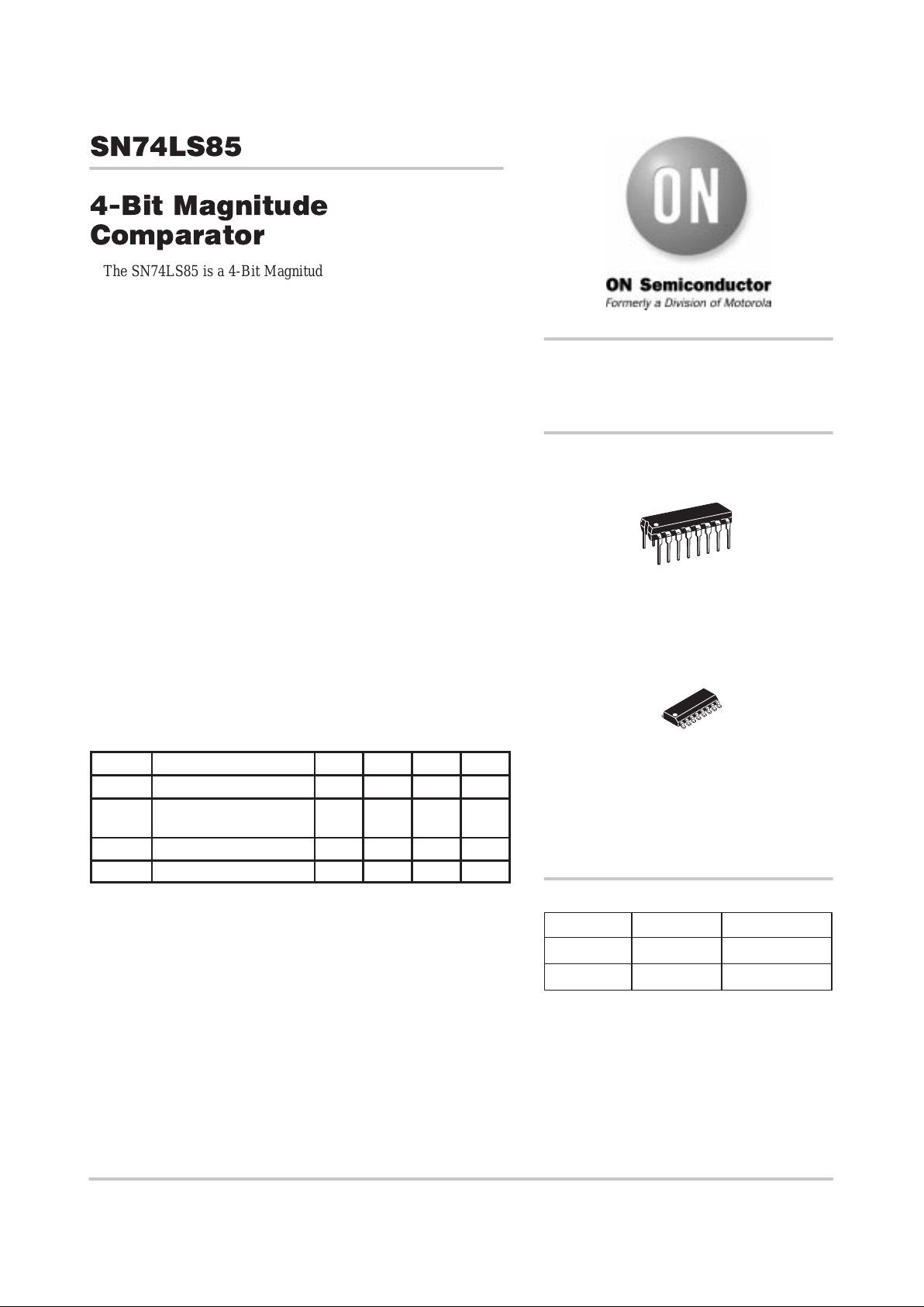
ORDERING INFORMATION
SN74LS85N 16 Pin DIP 2000 Units/Box
SN74LS85D 16 Pin
SOIC
D SUFFIX
CASE 751B
http://onsemi.com
2500/Tape & Reel
PLASTIC
N SUFFIX
CASE 648
16
1
16
1
Page 2
SN74LS85
http://onsemi.com
2
LOGIC SYMBOL
CONNECTION DIAGRAM DIP (TOP VIEW)
Parallel Inputs
A = B Expander Inputs
A < B, A > B, Expander Inputs
A Greater than B Output
B Greater than A Output
A Equal to B Output
A
0
– A3, B0 – B
3
I
A = B
I
A < B
, I
A > B
O
A > B
O
A < B
OA = B
1.5 U.L.
1.5 U.L.
0.5 U.L.
10 U.L.
10 U.L.
10 U.L.
0.75 U.L.
0.75 U.L.
0.25 U.L.
5 U.L.
5 U.L.
5 U.L.
NOTES:
a) 1 TTL Unit Load (U.L.) = 40 mA HIGH/1.6 mA LOW.
HIGH LOW
(Note a)LOADING
PIN NAMES
V
CC
= PIN 16
GND = PIN 8
10 12 13 15 9 11 14 1
4
2
3
5
7
6
A
0A1A2A3B0B1B2B3
I
A>B
I
A<B
I
A=B
O
A>B
O
A<B
O
A=B
NOTE:
The Flatpak version has the same
pinouts (Connection Diagram) as
the Dual In-Line Package.
14 13 12 11 10 9
123456
7
16 15
8
V
CC
B
3
A
3
B2A2A
1
A
0
B
1
B
0
I
A<BIA=BIA>BOA>BOA=B
O
A<B
GND
Page 3
H = HIGH Level
L = LOW Level
X = IMMATERIAL
SN74LS85
http://onsemi.com
3
LOGIC DIAGRAM
O
A>B
O
A<B
O
A=B
(5)
(6)
(7)
A3
B3
A2
B2
A<B
A=B
A>B
A1
B1
A0
B0
(15)
(1)
(13)
(14)
(12)
(11)
(10)
(9)
(2)
(3)
(4)
TRUTH TABLE
COMPARING INPUTS
CASCADING
INPUTS
OUTPUTS
A3,B3A2,B2A1,B1A0,B0I
A>BIA<BIA=B
O
A>B
O
A<B
O
A=B
A3>B
3
X X X X X X H L L
A3<B
3
XXXXXX L HL
A3=B3A2>B
2
XXXXX H LL
A3=B3A2<B
2
XXXXX L HL
A3=B3A2=B2A1>B
1
XXXX H LL
A3=B3A2=B2A1<B
1
XXXX L HL
A3=B3A2=B2A1=B1 A0>B
0
X XX H LL
A3=B3A2=B2A1=B1A0<B
0
X XX L HL
A3=B3A2=B2A1=B1A0=B
0
H LL H LL
A3=B3A2=B2A1=B1A0=B
0
L HL L HL
A3=B3A2=B2A1=B1A0=B
0
X XH L LH
A3=B3A2=B2A1=B1A0=B
0
H HL L LL
A3=B3A2=B2A1=B1A0=B
0
L L L H H L
Page 4

NOTE:
The SN74LS85 can be used as a 5-bit comparator only
when the outputs are used to drive the A
0–A3
and B0–B
3
inputs of another SN74LS85 as shown in Figure 2 in positions #1, 2, 3, and 4.
SN74LS85
http://onsemi.com
4
Figure 1. Comparing Two n-Bit Words
L = LOW LEVEL
H = HIGH LEVEL
A0A1A2A3B0B1B2B
3
A0A1A2A3B0B1B2B
3
A0A1A2A3B0B1B2B
3
L
L
H
I
A > B
I
A < B
I
A = B
O
A > B
O
A < B
O
A = B
I
A > B
I
A < B
I
A = B
O
A > B
O
A < B
O
A = B
A > B
A < B
A = B
SN74LS85 SN74LS85
An3An2An1AnBn3Bn2Bn1B
n
APPLICATIONS
Figure 2 shows a high speed method of comparing two
24-bit words with only two levels of device delay. With the
technique shown in Figure 1, six levels of device delay result
when comparing two 24-bit words. The parallel technique
can be expanded to any number of bits, see Table 1.
Table 1
WORD LENGTH NUMBER OF PKGS.
1–4 Bits 1
5–24 Bits 2–6
25–120 Bits 8–31
MSB = MOST SIGNIFICANT BIT
LSB = LEAST SIGNIFICANT BIT
L = LOW LEVEL
H = HIGH LEVEL
NC = NO CONNECTION
A0A1A2A3B0B1B2B
3
A0A1A2A3B0B1B2B
3
L
L
H
I
A > B
I
A < B
I
A = B
O
A > B
O
A < B
O
A = B
#5
(LSB)
INPUTS
A
0A1A2A3B0B1B2B3
I
A > B
I
A < B
I
A = B
O
A > B
O
A < B
O
A = B
#1
L
NC
A
20A21
B23B22B21B20A23A
22
A
19
B
19
(MSB)
A
5A6A7A8B5B6B7B8
A0A1A2A3B0B1B2B
3
I
A > B
I
A < B
I
A = B
O
A > B
O
A < B
O
A = B
#4
NC
L
A
4
B
4
A0A1A2A3B0B1B2B
3
I
A > B
I
A < B
I
A = B
O
A > B
O
A < B
O
A = B
#3
NC
L
A
9
B
9
A10A
11
B13B12B11B10A13A
12
A0A1A2A3B0B1B
2
B
3
I
A > B
I
A < B
I
A = B
O
A > B
O
A < B
O
A = B
#2
NC
L
A
14
B
14
A15A
16
B18B17B16B15A18A
17
OUTPUTS
A0A1A2A3B0B1B2B
3
I
A > B
I
A < B
I
A = B
O
A > B
O
A < B
O
A = B
#6
INPUTS
Figure 2. Comparison of Two 24-Bit Words
Page 5

SN74LS85
http://onsemi.com
5
DC CHARACTERISTICS OVER OPERATING TEMPERATURE RANGE (unless otherwise specified)
Limits
Symbol Parameter
Min Typ Max
Unit Test Conditions
V
IH
Input HIGH Voltage 2.0 V
Guaranteed Input HIGH Voltage for
All Inputs
V
IL
Input LOW Voltage
0.8
V
Guaranteed Input LOW Voltage for
All Inputs
V
IK
Input Clamp Diode Voltage –0.65 –1.5 V VCC = MIN, IIN = –18 mA
V
OH
Output HIGH Voltage
2.7 3.5 V VCC = MIN, IOH = MAX, VIN = V
IH
or V
IL
per Truth Table
p
0.25
0.4
V IOL = 4.0 mA
VCC = VCC MIN,
VOLOutput LOW Voltage
0.35 0.5 V
IOL = 8.0 mA
V
IN
=
V
IL
or
V
IH
per Truth Table
I
IH
Input HIGH Current
A < B, A > B
Other Inputs
20
60
µA VCC = MAX, VIN = 2.7 V
IH
A < B, A > B
Other Inputs
0.1
0.3
mA VCC = MAX, VIN = 7.0 V
I
IL
Input LOW Current
A < B, A > B
Other Inputs
–0.4
–1.2
mA VCC = MAX, VIN = 0.4 V
I
OS
Output Short Circuit Current (Note 1) –20 –100 mA VCC = MAX
I
CC
Power Supply Current 20 mA VCC = MAX
Note 1: Not more than one output should be shorted at a time, nor for more than 1 second.
AC CHARACTERISTICS (T
A
= 25°C, VCC = 5.0 V)
Limits
Symbol Parameter
Min Typ Max
Unit T est Conditions
t
PLH
t
PHL
Any A or B to A < B, A > B 24
20
36
30
ns
t
PLH
t
PHL
Any A or B to A = B 27
23
45
45
ns
t
PLH
t
PHL
A < B or A = B to A > B 14
11
22
17
ns
VCC = 5.0 V
C
L
= 15 pF
t
PLH
t
PHL
A = B to A = B 13
13
20
26
ns
t
PLH
t
PHL
A > B or A = B to A < B 14
11
22
17
ns
AC WAVEFORMS
Figure 3. Figure 4.
V
IN
V
OUT
1.3 V
t
PHL
1.3 V
1.3 V
1.3 V
t
PLH
V
IN
V
OUT
1.3 V
t
PHL
1.3 V
1.3 V 1.3 V
t
PLH
Page 6

SN74LS85
http://onsemi.com
6
P ACKAGE DIMENSIONS
N SUFFIX
PLASTIC PACKAGE
CASE 648–08
ISSUE R
NOTES:
1. DIMENSIONING AND TOLERANCING PER ANSI
Y14.5M, 1982.
2. CONTROLLING DIMENSION: INCH.
3. DIMENSION L TO CENTER OF LEADS WHEN
FORMED PARALLEL.
4. DIMENSION B DOES NOT INCLUDE MOLD FLASH.
5. ROUNDED CORNERS OPTIONAL.
–A–
B
F
C
S
H
G
D
J
L
M
16 PL
SEATING
18
916
K
PLANE
–T–
M
A
M
0.25 (0.010) T
DIM MIN MAX MIN MAX
MILLIMETERSINCHES
A 0.740 0.770 18.80 19.55
B 0.250 0.270 6.35 6.85
C 0.145 0.175 3.69 4.44
D 0.015 0.021 0.39 0.53
F 0.040 0.70 1.02 1.77
G 0.100 BSC 2.54 BSC
H 0.050 BSC 1.27 BSC
J 0.008 0.015 0.21 0.38
K 0.110 0.130 2.80 3.30
L 0.295 0.305 7.50 7.74
M 0 10 0 10
S 0.020 0.040 0.51 1.01
____
Page 7

SN74LS85
http://onsemi.com
7
P ACKAGE DIMENSIONS
D SUFFIX
PLASTIC SOIC PACKAGE
CASE 751B–05
ISSUE J
NOTES:
1. DIMENSIONING AND TOLERANCING PER ANSI
Y14.5M, 1982.
2. CONTROLLING DIMENSION: MILLIMETER.
3. DIMENSIONS A AND B DO NOT INCLUDE
MOLD PROTRUSION.
4. MAXIMUM MOLD PROTRUSION 0.15 (0.006)
PER SIDE.
5. DIMENSION D DOES NOT INCLUDE DAMBAR
PROTRUSION. ALLOWABLE DAMBAR
PROTRUSION SHALL BE 0.127 (0.005) TOTAL
IN EXCESS OF THE D DIMENSION AT
MAXIMUM MATERIAL CONDITION.
18
16 9
SEATING
PLANE
F
J
M
R
X 45
_
G
8 PLP
–B–
–A–
M
0.25 (0.010) B
S
–T–
D
K
C
16 PL
S
B
M
0.25 (0.010) A
S
T
DIM MIN MAX MIN MAX
INCHESMILLIMETERS
A 9.80 10.00 0.386 0.393
B 3.80 4.00 0.150 0.157
C 1.35 1.75 0.054 0.068
D 0.35 0.49 0.014 0.019
F 0.40 1.25 0.016 0.049
G 1.27 BSC 0.050 BSC
J 0.19 0.25 0.008 0.009
K 0.10 0.25 0.004 0.009
M 0 7 0 7
P 5.80 6.20 0.229 0.244
R 0.25 0.50 0.010 0.019
____
Page 8

SN74LS85
http://onsemi.com
8
ON Semiconductor and are trademarks of Semiconductor Components Industries, LLC (SCILLC). SCILLC reserves the right to make changes
without further notice to any products herein. SCILLC makes no warranty , representation or guarantee regarding the suitability of its products for any particular
purpose, nor does SCILLC assume any liability arising out of the application or use of any product or circuit, and specifically disclaims any and all liability ,
including without limitation special, consequential or incidental damages. “Typical” parameters which may be provided in SCILLC data sheets and/or
specifications can and do vary in different applications and actual performance may vary over time. All operating parameters, including “Typicals” must be
validated for each customer application by customer’s technical experts. SCILLC does not convey any license under its patent rights nor the rights of others.
SCILLC products are not designed, intended, or authorized for use as components in systems intended for surgical implant into the body, or other applications
intended to support or sustain life, or for any other application in which the failure of the SCILLC product could create a situation where personal injury or
death may occur. Should Buyer purchase or use SCILLC products for any such unintended or unauthorized application, Buyer shall indemnify and hold
SCILLC and its officers, employees, subsidiaries, affiliates, and distributors harmless against all claims, costs, damages, and expenses, and reasonable
attorney fees arising out of, directly or indirectly , any claim of personal injury or death associated with such unintended or unauthorized use, even if such claim
alleges that SCILLC was negligent regarding the design or manufacture of the part. SCILLC is an Equal Opportunity/Affirmative Action Employer .
PUBLICATION ORDERING INFORMATION
ASIA/PACIFIC: LDC for ON Semiconductor – Asia Support
Phone: 303–675–2121 (Tue–Fri 9:00am to 1:00pm, Hong Kong Time)
T oll Free from Hong Kong 800–4422–3781
Email: ONlit–asia@hibbertco.com
JAPAN: ON Semiconductor, Japan Customer Focus Center
4–32–1 Nishi–Gotanda, Shinagawa–ku, T okyo, Japan 141–8549
Phone: 81–3–5487–8345
Email: r14153@onsemi.com
Fax Response Line: 303–675–2167
800–344–3810 Toll Free USA/Canada
ON Semiconductor Website: http://onsemi.com
For additional information, please contact your local
Sales Representative.
SN74LS85/D
North America Literature Fulfillment:
Literature Distribution Center for ON Semiconductor
P.O. Box 5163, Denver, Colorado 80217 USA
Phone: 303–675–2175 or 800–344–3860 T oll Free USA/Canada
Fax: 303–675–2176 or 800–344–3867 Toll Free USA/Canada
Email: ONlit@hibbertco.com
N. American Technical Support: 800–282–9855 Toll Free USA/Canada
EUROPE: LDC for ON Semiconductor – European Support
German Phone: (+1) 303–308–7140 (M–F 2:30pm to 5:00pm Munich Time)
Email: ONlit–german@hibbertco.com
French Phone: (+1) 303–308–7141 (M–F 2:30pm to 5:00pm Toulouse Time)
Email: ONlit–french@hibbertco.com
English Phone: (+1) 303–308–7142 (M–F 1:30pm to 5:00pm UK Time)
Email: ONlit@hibbertco.com
 Loading...