

Page 1
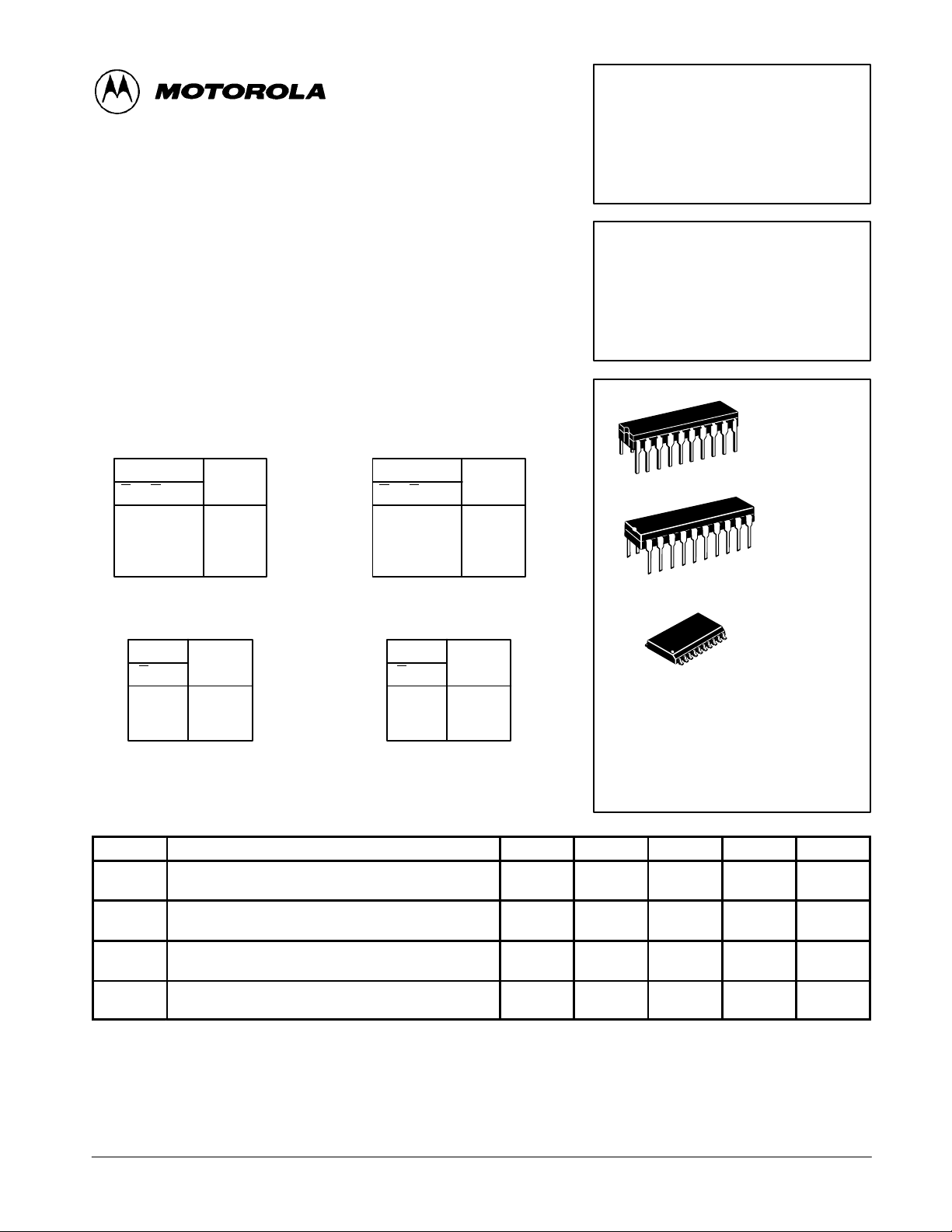
SN54/74LS795
SN54/74LS796
TRI-STATE OCTAL BUFFERS
The SN54/74LS795 thru SN54/74LS798 device types provide a second
source for the 71/81LS95 thru 71 /81LS98 series. These devices are octal
low power Schottky versions of the 70/8095 thru 70/8098 3-STATE Hex
Buffers. The LS795 and LS797 are noninverting and the LS796 and LS798
are inverting functions. On each buffer, one of the two inputs is used as a
control line to gate the output into the high impedance state, while the other
input passes the data through the buffer . On the LS795 and LS796 access is
through a 2-input NOR gate, with all eight 3-ST A TE enable lines common. On
the LS797 and LS798, four buffers are enabled from one common line and the
other four buffers from another common line. On all device types the 3-ST ATE
condition is achieved by applying a high logic level to the enable pins.
TRUTH TABLES
LS795
INPUTS OUTPUT
G
1G2A Y
H
X
H
L
L
X
X
H
L
X
L
L
G
Z
Z
H
L
LS796
INPUTS OUTPUT
1G2A Y
H
X
X
L
L
H
L
L
X
X
H
L
Z
Z
L
H
SN54/74LS797
SN54/74LS798
TRI-STATE OCTAL BUFFERS
LOW POWER SCHOTTKY
J SUFFIX
CERAMIC
20
1
20
1
CASE 732-03
N SUFFIX
PLASTIC
CASE 738-03
LS797
INPUTS OUTPUT
G
AY
H
X
L
H
L
L
Z
H
L
LS798
INPUTS OUTPUT
G
AY
H
X
L
H
L
L
Z
L
H
DW SUFFIX
20
1
CASE 751D-03
ORDERING INFORMATION
SN54LSXXXJ Ceramic
SN74LSXXXN Plastic
SN74LSXXXDW SOIC
SOIC
GUARANTEED OPERATING RANGES
Symbol Parameter Min Typ Max Unit
V
T
I
I
CC
A
OH
OL
Supply Voltage 54
74
Operating Ambient Temperature Range 54
74
Output Current — High 54
74
Output Current — Low 54
74
4.5
4.75
–55
0
5.0
5.0
25
25
5.5
5.25
125
70
–2.6
–5.0
8.0
16
V
°C
mA
mA
FAST AND LS TTL DAT A
5-1
Page 2
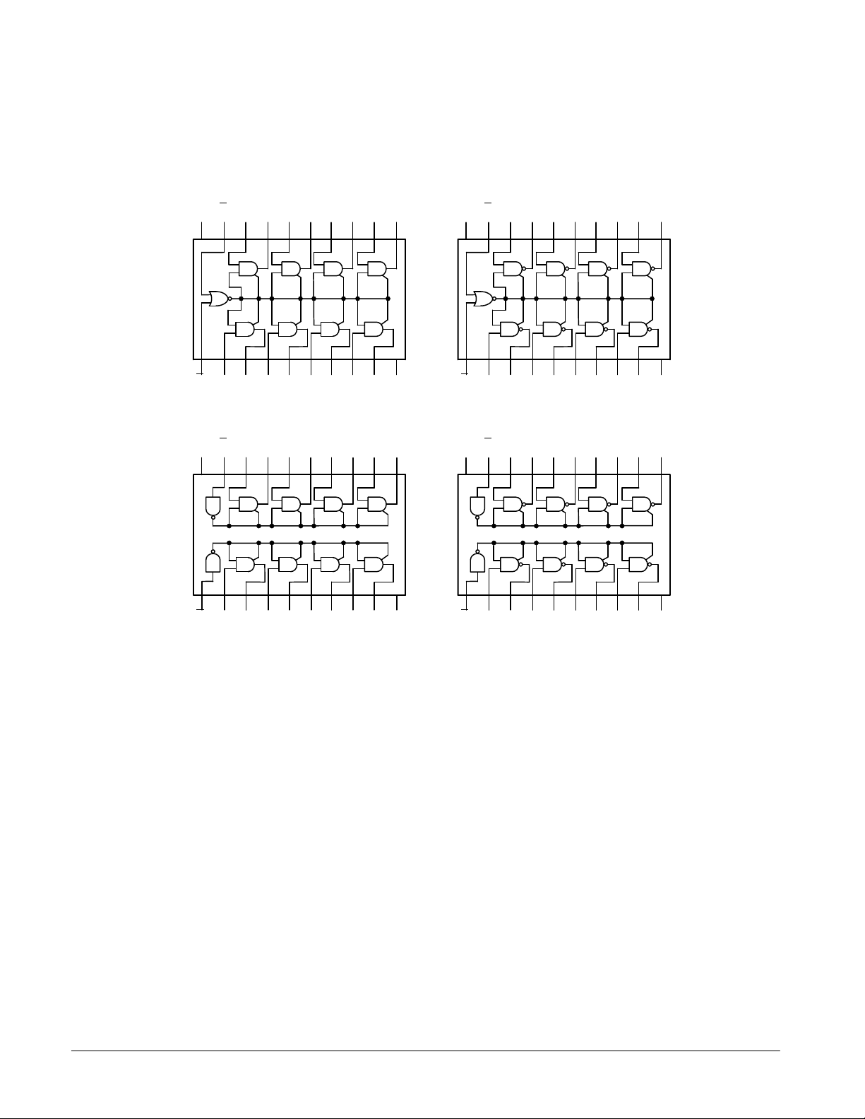
LOGIC DIAGRAMS
SN54/74LS795 • SN54/74LS796
SN54/74LS797 • SN54/74LS798
VCCG2
G
A8 Y8 A7 Y7 A6 Y6 A5 Y5
20 19 18 17 16 15 14 13 12 11
123456789 10
1
A1 Y1 A2 Y2 A3 Y3 A4 Y4 GND
SN54/74LS795
VCCG2
G
A8 Y8 A7 Y7 A6 Y6 A5 Y5
20 19 18 17 16 15 14 13 12 11
12345678910
1
A1 Y1 A2 Y2 A3 Y3 A4 Y4 GND
SN54/74LS797
VCCG2
G
A8 Y8 A7 Y7 A6 Y6 A5 Y5
20 19 18 17 16 15 14 13 12 11
123 456789 10
1
A1 Y1 A2 Y2 A3 Y3 A4 Y4 GND
SN54/74LS796
VCCG2
G
A8 Y8 A7 Y7 A6 Y6 A5 Y5
20 19 18 17 16 15 14 13 12 11
123 456789 10
1
A1 Y1 A2 Y2 A3 Y3 A4 Y4 GND
SN54/74LS798
FAST AND LS TTL DATA
5-2
Page 3
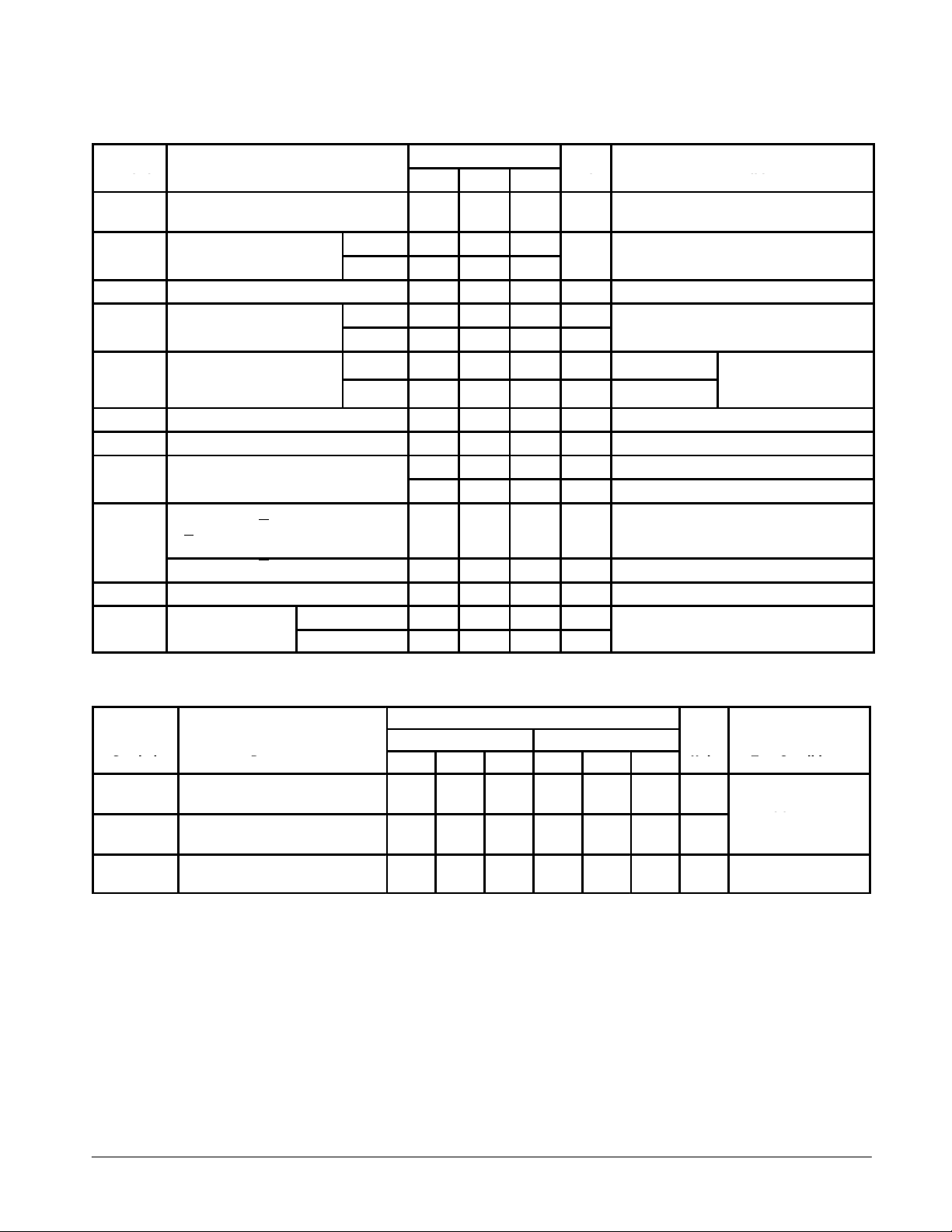
SN54/74LS795 THRU SN54/74LS798
VILI
LOW Volt
V
pg
VOHOutput HIGH Volt
V
MIN, I
MAX
VOLOutput LOW Volt
V
V
V
IIHI
HIGH C
t
I
pp y
V
MAX
CC
DC CHARACTERISTICS OVER OPERATING TEMPERATURE RANGE (unless otherwise specified)
Limits
Symbol Parameter
V
IH
V
IK
I
OZH
I
OZL
I
IL
I
OS
CC
Note 1: Not more than one output should be shorted at a time, nor for more than 1 second.
Input HIGH Voltage 2.0 V
nput
Input Clamp Diode Voltage –0.65 –1.5 V VCC = MIN, IIN = –18 mA
Output Off Current — HIGH 20 µA VCC = MAX, V
Output Off Current — LOW –20 µA VCC = MAX, V
nput
Input LOW Current
A Input, Both G
G
Input
A Input, Both G at 2.0 V –20 µA VCC = MAX, VIN = 0.5 V
Short Circuit Current (Note 1) –30 –130 mA VCC = MAX
Power Supply
Current
age
age
age
urren
at 0.4 V
LS795/LS797
LS795/LS798
54 0.7
74 0.8
54 2.5 3.5 V
74 2.7 3.5 V
54, 74 0.25 0.4 V IOL = 8.0 mA
74 0.35 0.5 V IOL = 16 mA
Min Typ Max
20 µA VCC = MAX, VIN = 2.7 V
–0.1 mA VCC = MAX, VIN = 7.0 V
–0.4
–0.4
26
21
Unit Test Conditions
Guaranteed Input HIGH Voltage for
All Inputs
Guaranteed Input LOW Voltage for
All Inputs
=
CC
mA VCC = MAX, VIN = 0.4 V
mA
mA
CC
=
=
OH
VCC = VCC MIN,
IN
per Truth Table
= 2.7 V
OUT
= 0.4 V
OUT
=
or
IL
IH
AC CHARACTERISTICS (T
Symbol Parameter
t
PLH
t
PHL
t
PZH
t
PZL
t
PHZ
t
PLZ
Propagation Delay
Output Enable Time
Output Disable Time
= 25°C)
A
Limits
LS795/LS797 LS796/LS798
Min Typ Max Min Typ Max
11
15
16
13
13
19
16
22
25
20
20
27
6.0
13
17
16
13
18
10
17
27
25
20
27
Unit Test Conditions
ns
ns
ns CL = 5.0 pF
VCC = 5.0 V
CL = 15 pF
FAST AND LS TTL DATA
5-3
 Loading...