

Page 1
SYNCHRONOUS 4-BIT
UP/DOWN COUNTER
The SN54/74LS669 is a synchronous 4-bit up/down counter. The LS669 is
a 4-bit binary counter. For high speed counting applications, this presettable
counter features an internal carry lookahead for cascading purposes. By
clocking all flip-flops simultaneously so the outputs change coincident with
each other (when instructed to do so by the count enable inputs and internal
gating) synchronous operation is provided. This helps to eliminate output
counting spikes, normally associated with asynchronous (ripple-clock) counters. The four master-slave flip-flops are triggered on the rising (positive-going)
edge of the clock waveform by a buffered clock input.
Circuitry of the load inputs allows loading with the carry-enable output of the
cascaded counters. Because loading is synchronous, disabling of the counter
by setting up a low level on the load input will cause the outputs to agree with
the data inputs after the next clock pulse.
Cascading counters for N-bit synchronous applications are provided by the
carry look-ahead circuitry, without additional gating. T wo count-enable inputs
and a carry output help accomplish this function. Count-enable inputs (P
T
) must both be low to count. The level of the up-down input determines the
direction of the count. When the input level is low, the counter counts down,
and when the input is high, the count is up. Input T
is fed forward to enable the
carry output. The carry output will now produce a low level output pulse with a
duration ≈ equal to the high portion of the QA output when counting up and
when counting down ≈ equal to the low portion of the QA output. This low level
carry pulse may be utilized to enable successive cascaded stages. Regardless of the level of the clock input, transitions at the P
or T inputs are allowed.
By diode-clamping all inputs, transmission line effects are minimized which
allows simplification of system design.
Any changes at control inputs (ENABLE P
, ENABLE T , LOAD, UP/DOWN)
will have no effect on the operating mode until clocking occurs because of the
fully independant clock circuits. Whether enabled, disabled, loading or counting, the function of the counter is dictated entirely by the conditions meeting
the stable setup and hold times.
• Programmable Look-Ahead Up/Down Binary/Decade Counters
• Fully Synchronous Operation for Counting and Programming
• Internal Look-Ahead for Fast Counting
• Carry Output for n-Bit Cascading
• Fully Independent Clock Circuit
• Buffered Outputs
and
SN54/74LS669
SYNCHRONOUS 4-BIT
UP/DOWN COUNTER
LOW POWER SCHOTTKY
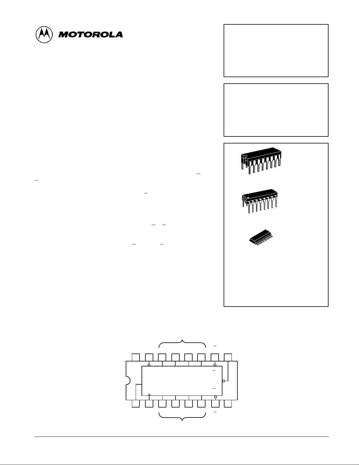
J SUFFIX
CERAMIC
16
1
16
1
16
1
ORDERING INFORMATION
SN54LSXXXJ Ceramic
SN74LSXXXN Plastic
SN74LSXXXD SOIC
CASE 620-09
N SUFFIX
PLASTIC
CASE 648-08
D SUFFIX
SOIC
CASE 751B-03
CONNECTION DIAGRAM (TOP VIEW)
RIPPLE
CARRY
OUTPUT
V
CC
16 15
RIPPLE
CARRY
OUTPUT
UP/DOWN
CK A B C D
123456
CK A B C D ENABLE
U/D
OUTPUTS
ENABLE
T
QAQBQ
14 13 12 11 10 9
QAQBQCQ
DATA INPUTS
Q
D
C
ENABLE
D
T
LOAD
ENABLE
P
7
P
FAST AND LS TTL DAT A
5-1
LOAD
8
GND
Page 2
(9)
(7)
(10)
(1)
LOAD
ENP
ENT
U/D
SN54/74LS669
LOGIC DIAGRAM
(3) (4) (5) (6)
DATA DATA DATA DATA
P
0
P
1
P
2
P
3
RCO
(15)
(RIPPLE CARRY
OUTPUT)
(2)
CP
CP D CP D CP D CP D
Q
A
(14) (13) (12) (11)
Q
B
Q
C
Q
D
GUARANTEED OPERATING RANGES
Symbol Parameter Min Typ Max Unit
V
T
I
OH
I
OL
CC
A
Supply Voltage 54
74
Operating Ambient Temperature Range 54
74
Output Current — High 54, 74 –0.4 mA
Output Current — Low 54
74
4.5
4.75
–55
0
5.0
5.0
25
25
5.5
5.25
125
70
4.0
8.0
V
°C
mA
FAST AND LS TTL DATA
5-2
Page 3

SN54/74LS669
VILI
LOW Volt
V
pg
VOHOutput HIGH Volt
CC
,
OH
,
IN IH
VOLOutput LOW Volt
V
V
V
V
MAX, V
V
IIHI
HIGH C
t
V
MAX, V
V
IILI
LOW C
t
V
MAX, V
V
V
5.0 V
DC CHARACTERISTICS OVER OPERATING TEMPERATURE RANGE (unless otherwise specified)
Limits
Symbol Parameter
V
IH
V
IK
I
OS
I
CC
Note 1: Not more than one output should be shorted at a time, nor for more than 1 second.
Input HIGH Voltage 2.0 V
nput
Input Clamp Diode Voltage –0.65 –1.5 V VCC = MIN, IIN = –18 mA
nput
nput
Short Circuit Current (Note 1) –20 –100 mA VCC = MAX
Power Supply Current 34 mA VCC = MAX
age
age
age
urren
urren
54
74
54 2.5 3.5 V
74 2.7 3.5 V
54, 74 0.25 0.4 V IOL = 4.0 mA
74 0.35 0.5 V IOL = 8.0 mA
Others 20 µA
Enable T 40 µ A
Others 0.1 mA
Enable T 0.2 mA
Others –0.4 mA
Enable T –0.8 mA
Min Typ Max
0.7
0.8
Unit Test Conditions
Guaranteed Input HIGH Voltage for
All Inputs
Guaranteed Input LOW Voltage for
All Inputs
VCC = MIN, IOH = MAX, VIN = V
or VIL per Truth Table
=
CC
=
CC
=
CC
VCC = VCC MIN,
=
IN
per Truth Table
= 2.7
IN
= 7.0
IN
= 0.4
IN
IH
or
IL
IH
AC CHARACTERISTICS (T
Symbol Parameter
f
MAX
t
PLH
t
PHL
t
PLH
t
PHL
t
PLH
t
PHL
t
PLH
t
PHL
Maximum Clock Frequency 25 32 MHz
Propagation Delay,
Clock to RCO
Propagation Delay,
Clock to Any Q
Enable to RCO
U/D to RCO
= 25°C, VCC = 5.0 V)
A
AC SETUP REQUIREMENTS (T
Symbol Parameter
t
W
t
s
t
s
t
s
t
s
t
h
Clock Pulse Width 20 ns
Data Setup Time 20 ns
Enable Setup Time 35 ns
Load Setup Time 25 ns
U/D Setup Time 30 ns
Hold Time, Any Input 0 ns
= 25°C)
A
Limits
Min Typ Max
26
40
18
18
11
29
22
26
Limits
Min Typ Max
40
60
27
27
17
45
35
40
Unit T est Conditions
ns
ns
ns
ns
Unit T est Conditions
CL = 15 pF
=
CC
FAST AND LS TTL DATA
5-3
Page 4

SN54/74LS669
PARAMETER MEASUREMENT INFORMATION
CLOCK
INPUT
LOAD
INPUT
DATA INPUTS
A,B,C, and D
ENABLE P
ENABLE T
UP/DOWN
INPUT
or
t
w(clock)
1.3 V 1.3 V 1.3 V 1.3 V 1.3 V
t
t
s
1.3 V
t
w(clock)
t
s
t
h
t
h
s
1.3 V1.3 V
1.3 V
t
s
1.3 V
t
s
1.3 V 1.3 V 1.3 V
t
h
t
h
t
s
1.3 V
t
h
1.3 V
3 V
0 V
3 V
0 V
3 V
0 V
0 V
3 V
3 V
0 V
ENABLE T
INPUT
RIPPLE
CARRY
OUTPUT
1.3 V
t
PHL
VOLTAGE WAVEFORMS
1.3 V
t
PLH
1.3 V 1.3 V
3 V
0 V
V
V
OL
OH
FAST AND LS TTL DATA
5-4
 Loading...