

Page 1
OCTAL BUS TRANSCEIVER
WITH 3-STATE OUTPUT
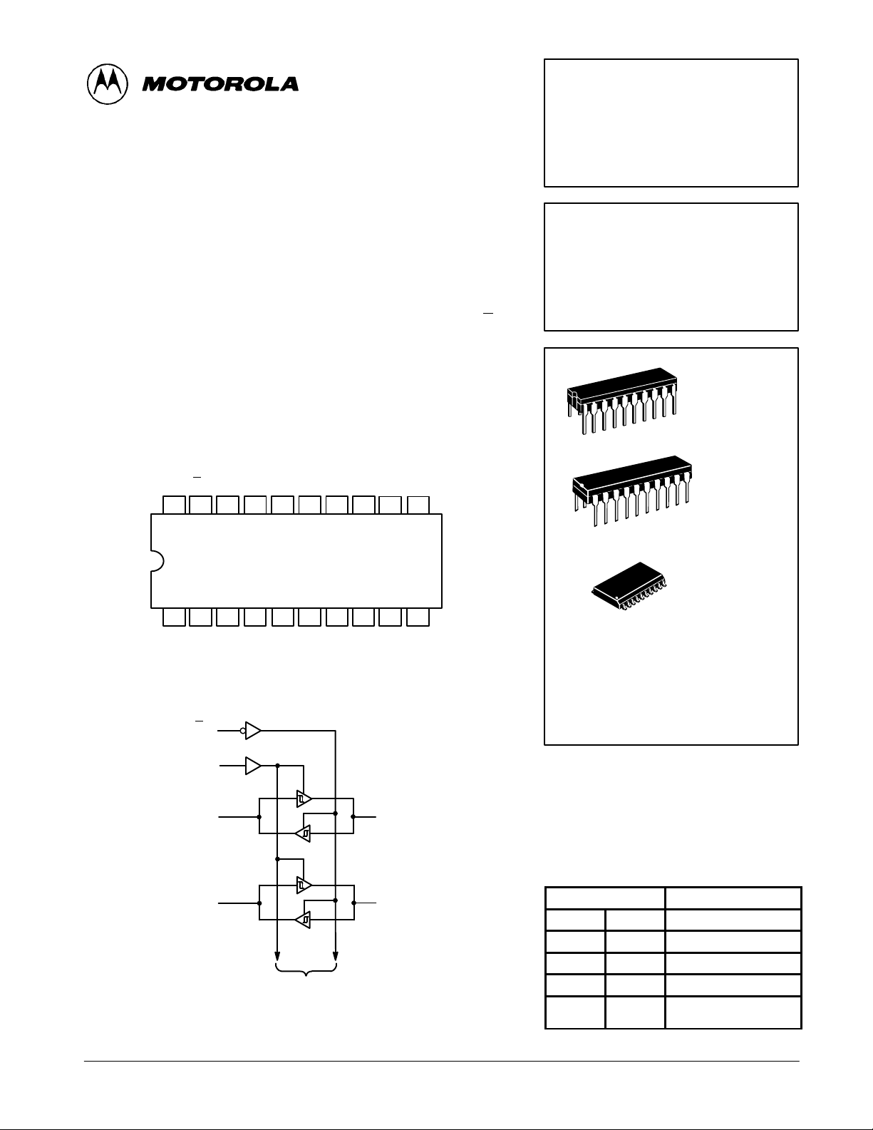
The SN54/74LS623 series is an octal bus transceiver designed for
asynchronous two-way communication between data buses. Control function
implementation allows maximum timing flexibility . Enable inputs may be used
to disable the device so that buses are effectively isolated. Depending on the
Logic Levels at the enable inputs, Data transmission is allowed from the A bus
to the B bus or from the B bus to the A bus. The dual-enable configuration
gives the LS623 the capability to store data by simultaneous enabling of G
and GAB. Each output reinforces its input in this transceiver configuration.
Thus, when both control inputs are enabled all other data sources to the two
sets of bus lines (16 in all) will remain at their last states.
CONNECTION DIAGRAM (TOP VIEW)
ENABLE
BA
V
CC
20 19
G
B1 B2 B3 B5B4 B6
18 17 16 15 14 13
B7 B8
12 11
BA
SN54/74LS623
OCT AL BUS TRANSCEIVER
WITH 3-STATE OUTPUT
LOW POWER SCHOTTKY
20
1
20
1
CASE 732-03
CASE 738-03
J SUFFIX
CERAMIC
N SUFFIX
PLASTIC
123456
A1 A2 A3 A4 A5 A6 A7
ENABLE
GAB
BLOCK DIAGRAM
1/4 LS623
BA
G
GAB
A1
A2
TO OTHER SIX
TRANSCEIVERS
7
8
B1
B2
910
A8 GND
DW SUFFIX
20
1
SOIC
CASE 751D-03
ORDERING INFORMATION
SN54LSXXXJ Ceramic
SN74LSXXXN Plastic
SN74LSXXXDW SOIC
FUNCTION TABLE
ENABLE INPUTS OPERATION
GBA GAB LS623
L L B data to A bus
H H A data to B bus
H L Isolation
B data to A bus,
L H
H = HIGH Level, L = LOW Level, X = Irrelevant
A data to B bus
FAST AND LS TTL DATA
5-1
Page 2
SN54/74LS623
VILI
LOW Volt
V
pg
VOHOutput HIGH Volt
VOLOutput LOW Volt
V
V
V
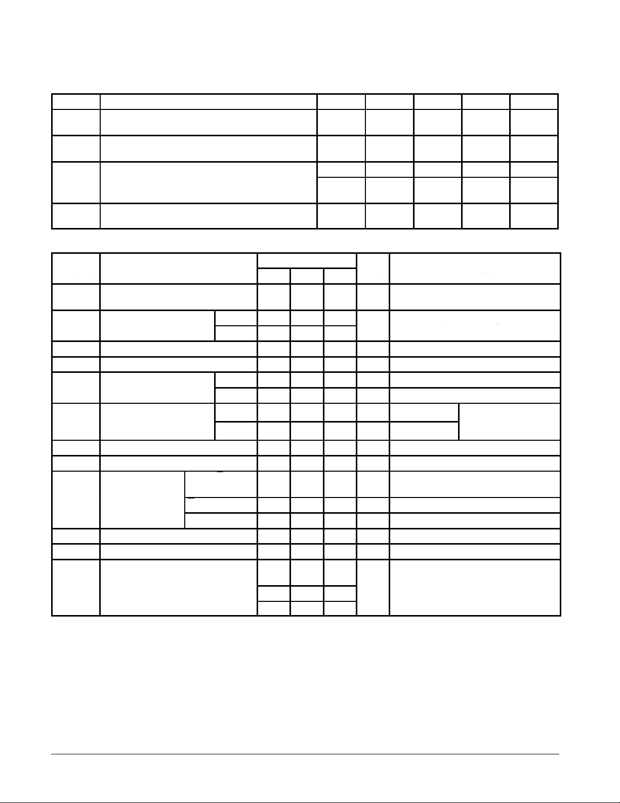
GUARANTEED OPERATING RANGES
Symbol Parameter Min Typ Max Unit
V
CC
T
A
I
OH
I
OL
DC CHARACTERISTICS OVER OPERATING TEMPERATURE RANGE (unless otherwise specified)
Symbol Parameter
V
IH
VT+–VT– Hysteresis 0.2 0.4 V VCC = MIN
V
IK
I
OZH
I
OZL
I
IH
I
IL
I
OS
I
CC
Note 1: Not more than one output should be shorted at a time, nor for more than 1 second.
Supply Voltage 54
Operating Ambient Temperature Range 54
Output Current — High
Output Current — Low 54
Limits
Min Typ Max
Input HIGH Voltage 2.0 V
nput
Input Clamp Diode Voltage –0.65 –1.5 V VCC = MIN, IIN = –18 mA
Output Off Current HIGH 20 µA VCC = MAX, V
Output Off Current LOW –400 µA VCC = MAX, V
Input HIGH Current
Input LOW Current –0.4 mA VCC = MAX, VIN = 0.4 V
Short Circuit Current (Note 1) –40 –225 mA VCC = MAX
Power Supply Current
Total Output HIGH
Total Output LOW
Total at HIGH Z
age
age
age
A, or B, GBA or
GAB
GAB or GAB
A or B
54 0.5
74 0.6
54, 74 2.4 3.4 V VCC = MIN, IOH = ± 3.0 mA
54, 74 2.0 V
54, 74 0.25 0.4 V IOL = 12 mA
74 0.35 0.5 V IOL = 24 mA
74
74
54, 74 –3.0 mA
54
74
74
20 µA VCC = MAX, VIN = 2.7 V
0.1 mA VCC = MAX, VIN = 7.0 V
0.1 mA VCC = MAX, VIN = 5.5 V
70
90
95
4.5
4.75
–55
0
Unit Test Conditions
Guaranteed Input HIGH Voltage for
All Inputs
Guaranteed Input LOW Voltage for
All Inputs
VCC = MIN, IOH = MAX
mA VCC = MAX
5.0
5.0
25
25
5.25
125
–12
–15
VCC = VCC MIN,
=
IN
per Truth Table
= 2.7 V
OUT
= 4.0 V
OUT
5.5
70
12
24
or
IL
IH
V
°C
mA
mA
FAST AND LS TTL DATA
5-2
Page 3
SN54/74LS623
L
p,
C
5.0 pF
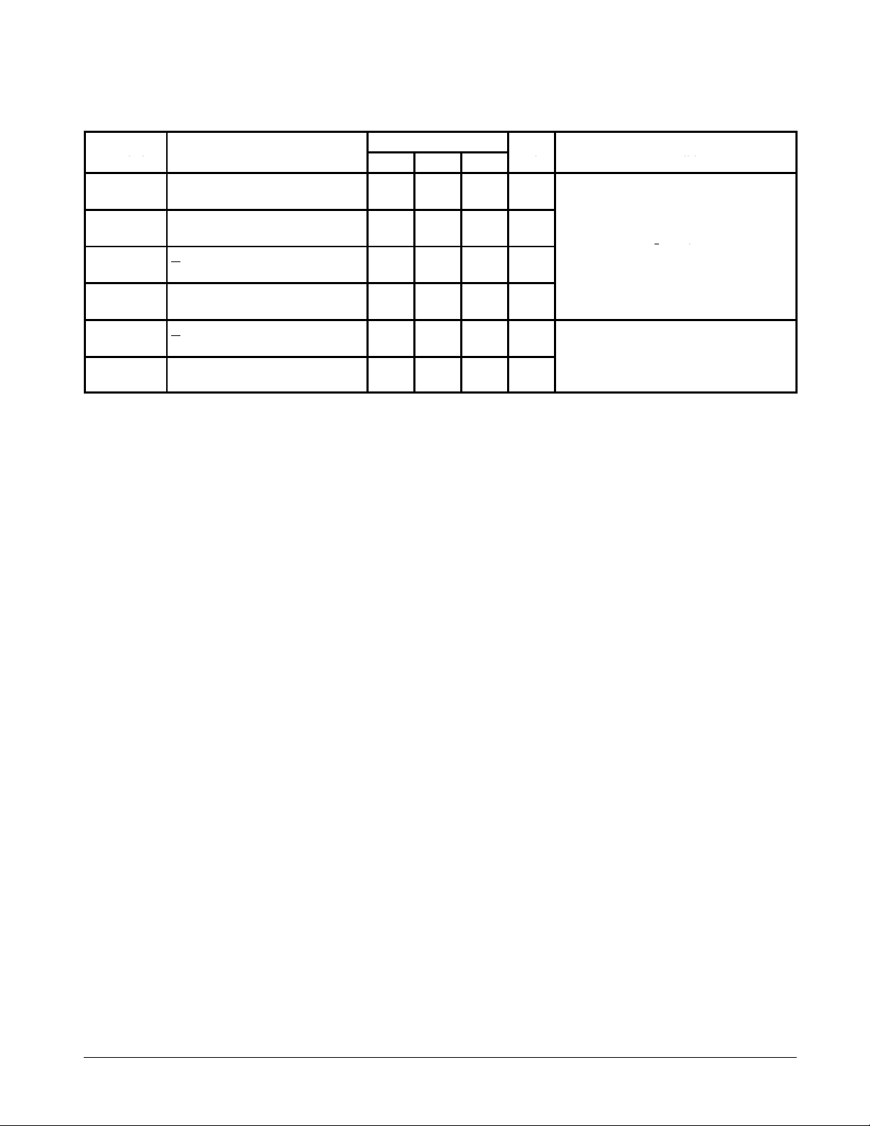
AC CHARACTERISTICS (T
Symbol Parameter
t
PLH
t
PHL
t
PLH
t
PHL
t
PZL
t
PZH
t
PZL
t
PZH
t
PLZ
t
PHZ
t
PLZ
t
PHZ
Propagation Delay
A to B
Propagation Delay
B to A
Output Enable Time
G
BA to A
Output Enable Time
GAB to B
Output Disable Time
G
BA to A
Output Disable Time
GAB to B
A
= 25°C, VCC = 5.0 V)
Limits
Min Typ Max
8.0
11
8.0
11
31
26
31
26
15
15
15
15
15
15
15
15
40
40
40
40
25
25
25
25
Unit Test Conditions
ns
ns
ns
ns
ns
ns
CL = 45 pF,
RL = 667 Ω
=
L
FAST AND LS TTL DATA
5-3
 Loading...