

Page 1
FOUR-BIT UP/DOWN COUNTER
WITH THREE-STATE OUTPUTS
The SN54 / 74LS569A is designed as programmable up/down BCD and
Binary counters respectively. These devices have 3-state outputs for use in
bus organized systems. With the exception of output enable (OE
asynchronous clear (ACLR
), all functions occur on the positive edge of the
clock pulse (CP).
When the LOAD
input is LOW, the outputs will be programmed by the
parallel data inputs (A, B, C, D) on the next clock edge. Enabling of the
counters occurs only when CEP
Direction of the count is controlled by the up-down input (U/D
and CET are LOW and LOAD is HIGH.
), HIGH counts
up and LOW counts down. High-speed counting and cascading is implemented by internal look-ahead carry logic and an active LOW ripple carry output
). On the LS569A, the RCO is LOW at binary 15 during up-count and
(RCO
during down-count it is also LOW at binary 0. During normal cascading
operation RCO
requisite. When counting and when RCO
connected to the succeeding block at CET is the only
is LOW, the clocked carry output
(CCO) provides a HIGH-LOW-HIGH pulse for a duration equal to the LOW
time of the clock pulse. Two active LOW reset lines are provided, a master
reset asynchronous clear (ACLR
a HIGH state, the output control (OE
) and a synchronous clear (SCLR). When in
) input forces the counter output into a
HIGH impedance state and when LOW, the counter outputs are enabled.
• ESD > 3500 Volts
) and
SN54/74LS569A
FOUR-BIT UP/DOWN COUNTER
WITH THREE-ST ATE OUTPUTS
LOW POWER SCHOTTKY
J SUFFIX
CERAMIC
20
1
20
1
CASE 732-03
N SUFFIX
PLASTIC
CASE 738-03
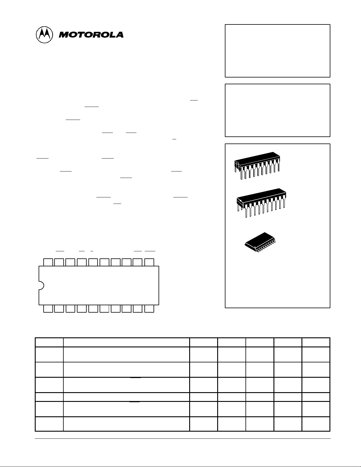
CONNECTION DIAGRAM (TOP VIEW)
RCO CCO OE Y
V
CC
20 19
123456
U/D
18 17 16 15 14 13
CP A B C D CEP
Y
A
B
Y
C
7
Y
D
8
ACLR
LOAD
CET
12 11
910
SCLR
GND
VCC = PIN 20
GND = PIN 10
Note: Pin 1 is marked
for orientation.
20
1
ORDERING INFORMATION
SN54LSXXXJ Ceramic
SN74LSXXXN Plastic
SN74LSXXXDW SOIC
DW SUFFIX
SOIC
CASE 751D-03
GUARANTEED OPERATING RANGES
Symbol Parameter Min Typ Max Unit
V
T
I
I
I
I
CC
A
OH
OH
OL
OL
Supply Voltage 54
74
Operating Ambient Temperature Range 54
74
Output Current — High Except RCO, CCO 54
74
Output Current — High RCO, CCO 54, 74 –0.44 mA
Output Current — Low Except RCO, CCO 54
74
Output Current — Low, RCO, CCO 54
74
4.5
4.75
–55
0
5.0
5.0
25
25
5.5
5.25
125
70
–1.0
–2.6
12
24
4.0
8.0
V
°C
mA
mA
mA
FAST AND LS TTL DAT A
5-1
Page 2
SN54/74LS569A
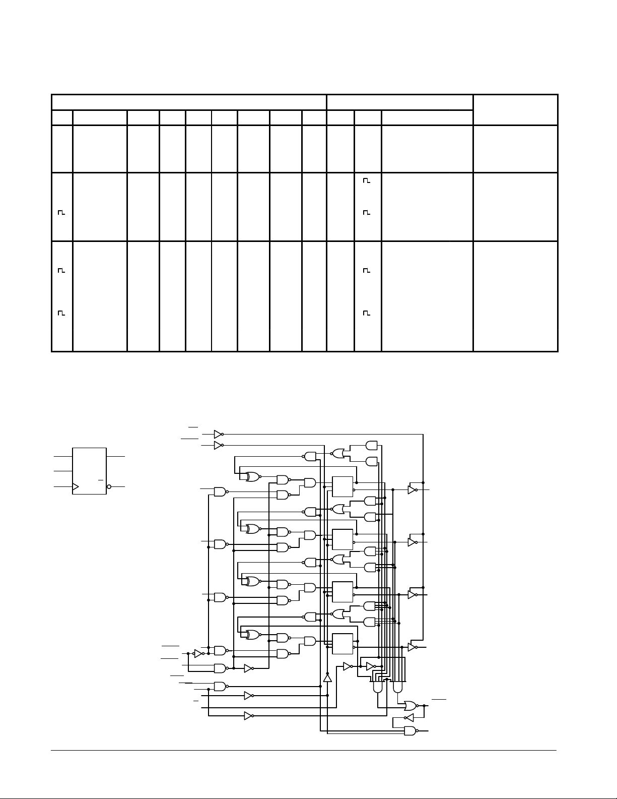
FUNCTION TABLE
INPUTS OUTPUTS
CP D C B A LOAD CET CEP U/D ACLR SCLR OE RCO CCO YDYCYBY
↑ X X X X H L L H H H L A/R A/R (QT – CP) + 1 Count Up
↑ X XXX H L L L H H L A/R A/R (QT – CP) – 1 Count Down
↑ X XXX H H X X H H L H H NC NC NC NC Count Inhibit
↑ X XXX H L H X H H L A/R H NC NC NC NC Count Inhibit
Ω X X X X X L L H H H L L H H H H Overflow
↑ X XXX X L H H H H L L H H H H H Overflow
↑ X XXX X H X H H H L H H H H H H Overflow Inhibit
X XXX X L L L H H L L L L L L Underflow
↑ X XXX X L H L H H L L H L L L L Underflow
↑ X XXX X H X L H H L H H L L L L Underflow Inhibit
↑ L H L H L X X X H H L H H L H L H Load Example
↑ X XXX X H X H H L L H H L L L L Clear (Synchronous)
X XXX X L L L H L L L L L L L Clear (Synchronous)
↑ X XXX X L H L H L L L H L L L L Clear (Synchronous)
↑ X XXX X H X L H L L H H L L L L Clear (Synchronous)
X X XXX X X X H L X L H H L L L L Asynchronous Clear
X XXX X L L L L X L L L L L L Asynchronous Clear
X X XXX X L H L L X L L H L L L L Asynchronous Clear
X X XXX X H X L L X L H H L L L L Asynchronous Clear
X X X X X X X X X X X H X X Hi-Z Output Disabled
(QT — CP) = Output state prior to clock edge A/R = Assumes required output state; X = Don’t care
NC = No change High except during Overflow and Underflow
A
D
R
CPQQ
LOGIC DIAGRAM
SCLR
LOAD
CEP
OE
ACLR
CET
CP
U/D
A
B
C
D
*
*
*
*
Y
A
Y
B
Y
C
Y
D
RCO
*
FAST AND LS TTL DATA
5-2
CCO
Page 3
SN54/74LS569A
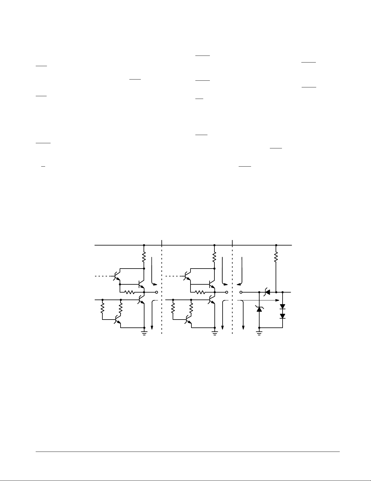
DEFINITION OF FUNCTIONAL TERMS
A, B, C, D The four programmable data inputs.
CEP
CET
Count Enable Trickle. Enables the ripple
CP Clock Pulse. All synchronous functions
LOAD
Enables parallel load of counter outputs
U/D
Up/Down Count Control. HIGH counts up
Count Enable Parallel. Can be used to
enable and inhibit counting in high speed
cascaded operation. CEP
must be LOW to
count.
carry output for cascaded operation. Must
be LOW to count.
occur on the LOW-to-HIGH transition of the
clock.
from data inputs on the next clock edge.
Must be HIGH to count.
and LOW counts down.
ACLR Asynchronous Clear. Master reset of
counters to zero when ACLR
is LOW,
independent of the clock.
SCLR Synchronous clear of counters to zero on
the next clock edge when SCLR
A HIGH on the output control sets the four
OE
is LOW.
counter outputs in the high impedance, and
a LOW, enables the output.
YA, YB, YC, YDThe four counter outputs.
Ripple Carry Output. Output will be LOW on
RCO
the maximum count on up-count. Upon
down-count, RCO
is LOW at 0000.
CCO Clock Carry Output. While counting and
RCO is LOW, CCO will follow the clock
HIGH-LOW-HIGH transition.
LOW-POWER SCHOTTKY INPUT/OUTPUT
CURRENT INTERFACE CONDITIONS
V
CC
DRIVING OUTPUT
I
OH
I
OL
Note: Actual current flow direction shown
DRIVING OUTPUT DRIVEN INPUT
I
I
OH
IL
I
I
OL
IH
FAST AND LS TTL DATA
5-3
Page 4
SN54/74LS569A
VILI
LOW Volt
V
pg
Output HIGH Volt
V
CC
,
OH
,
IN IH
,
VOLOutput LOW Volt
I
I
MAX
V
V
V
IIHI
HIGH C
t
IILI
LOW C
t
V
MAX, V
V
I
V
MAX
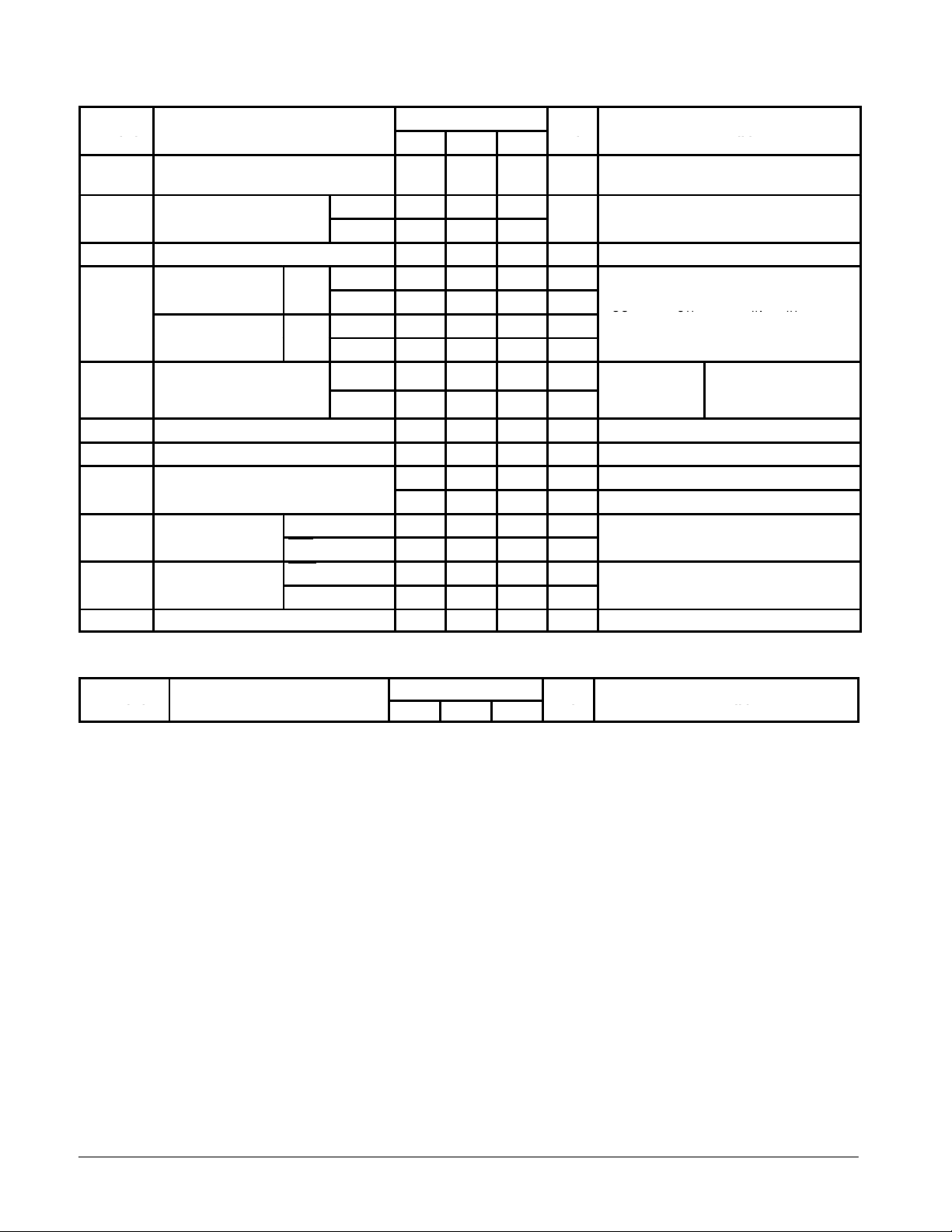
DC CHARACTERISTICS OVER OPERATING TEMPERATURE RANGE (unless otherwise specified)
Limits
Symbol Parameter
V
IH
V
IK
OH
I
OZH
I
OZL
OS
I
CC
Note 1: Not more than one output should be shorted at a time, nor for more than 1 second.
AC CHARACTERISTICS (T
Symbol Parameter
Input HIGH Voltage 2.0 V
nput
Input Clamp Diode Voltage –0.65 –1.5 V VCC = MIN, IIN = –18 mA
Output Off Current HIGH 20 µA VCC = MAX, VO = 2.7 V
Output Off Current LOW –20 µA VCC = MAX, VO = 0.4 V
nput
nput
Short Circuit Current
(Note 1)
Power Supply Current, 3-State 43 mA VCC = MAX
age
urren
urren
YA–
age
YD
RCO,
CCO
age
Others
CET
RCO, CCO –20
Others –30
= 25°C)
A
54 0.7
74 0.8
54 2.4 3.4 V
74 2.4 3.1 V
54 2.5 3.5 V
74 2.7 3.5 V
54, 74 0.25 0.4 V
74 0.35 0.5 V
Min Typ Max
20 µA VCC = MAX, VIN = 2.7 V
0.1 mA VCC = MAX, VIN = 7.0 V
–0.4 mA
–0.8 mA
–100 mA
–130 mA
Limits
Min Typ Max
Unit Test Conditions
Guaranteed Input HIGH Voltage for
All Inputs
Guaranteed Input LOW Voltage for
All Inputs
VCC = MIN, IOH = MAX, VIN = V
or VIL per Truth Table
=
CC
CC
=
=
OL
OL
Unit Test Conditions
VCC = VCC MIN,
=
IN
per Truth Table
= 0.4
IN
IH
or
IL
IH
FAST AND LS TTL DATA
5-4
Page 5
f
CC
MAX
t
PLH
t
PHL
t
PLH
t
PHL
t
PLH
t
PHL
t
PLH
t
PHL
t
PLH
t
PHL
t
PLH
t
PHL
t
PLH
t
PHL
t
PLH
t
PHL
t
PZH
t
PZL
t
PHZ
t
PLZ
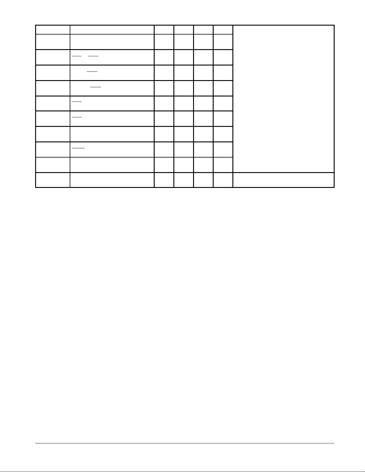
Maximum Toggle Frequency 35 MHz
Propagation Delay
Clock to Q
Propagation Delay
CET
to RCO
Propagation Delay
U/D to RCO
Propagation Delay
Clock to RCO
Propagation Delay
CET
to CCO
Propagation Delay
CEP
to CCO
Propagation Delay
Clock to CCO
Propagation Delay
ACLR
to Q
Output Enable Time
Output Disable Time
15
20
14
15
20
24
20
25
16
28
16
26
15
17
22
32
15
20
20
27
ns
ns
ns
ns
ns
ns
ns
ns
ns
ns CL = 5.0 pF
VCC = 5.0 V
CL = 45 pF
RL = 667 Ω
FAST AND LS TTL DATA
5-5
Page 6
SN54/74LS569A
V
V
AC SETUP REQUIREMENTS (T
Symbol Parameter
t
W
t
s
t
s
t
s
t
s
t
s
t
h
t
rec
LOAD1U/D1COUNT1ACLR1OE
Clock Pulse Width (Low) 20 ns
Setup Time, A, B, C, D 20 ns
Setup Time, SCLR 20 ns
Setup Time, LOAD 25 ns
Setup Time, U/D 30 ns
Setup Time, CET, CEP 20 ns
Hold Time, Any Inputs 0 ns
ACLR 15 ns
= 25°C, VCC = 5.0 V)
A
Limits
Min Typ Max
Unit Test Conditions
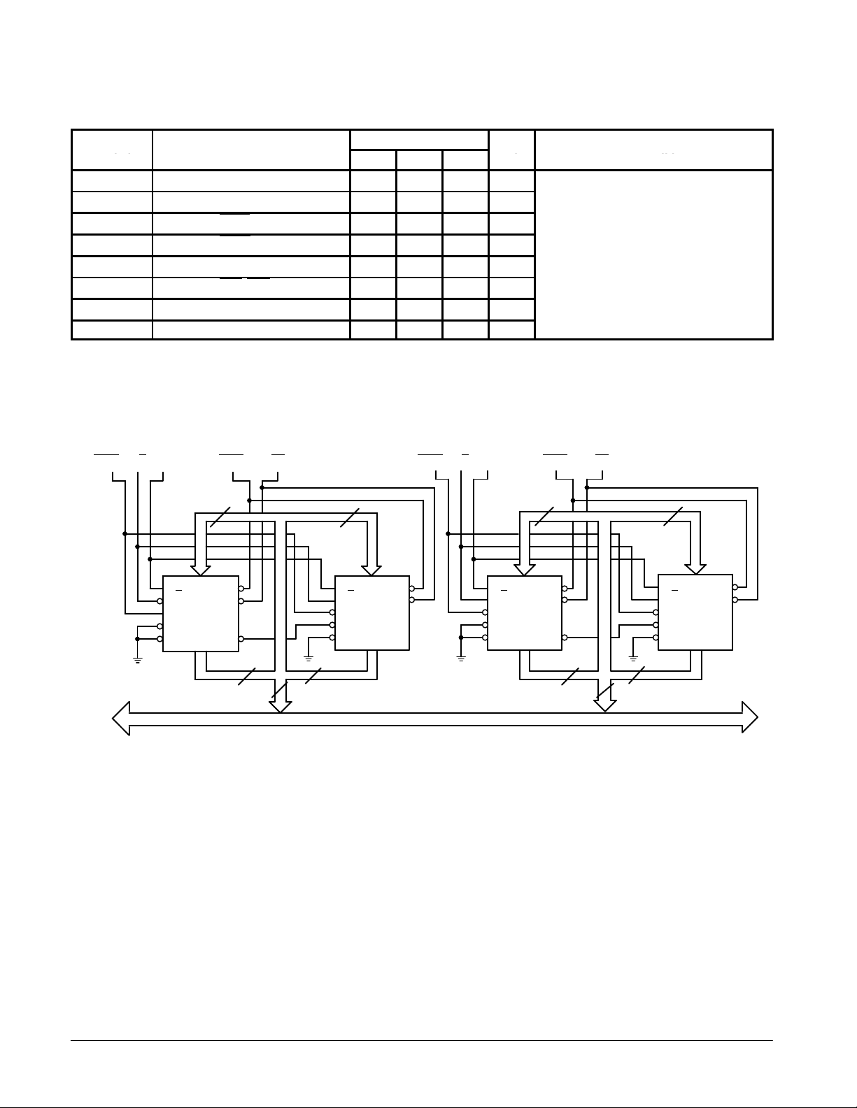
MICROPROGRAMMABLE DUAL-EVENT 8-BIT COUNTERS
1
LOAD2U/D2COUNT2ACLR2OE
= 5.0
CC
2
CP
U/D
LOAD
CET
CEP
44 44
A–D
LS569A
Y
A–D
ACLR
OE
RCO
44 4 4
CP
U/D
LOAD
CET
CEP
A–D
Y
A–D
ACLR
OE
LS569A
8–BIT BUS
CP
U/D
LOAD
CET
CEP
A–D
Y
A–D
ACLR
OE
LS569A
RCO
A–D
Y
A–D
ACLR
OE
LS569A
CP
U/D
LOAD
CET
CEP
88
FAST AND LS TTL DATA
5-6
 Loading...