

Page 1
4-BIT SHIFT REGISTER
WITH 3-STATE OUTPUTS
The SN74LS395 is a 4-Bit Register with 3-state outputs and can operate
in either a synchronous parallel load or a serial shift-right mode, as
determined by the Select input. An asynchronous active LOW Master Reset
(MR) input overrides the synchronous operations and clears the register. An
active HIGH Output Enable (OE) input controls the 3-state output buffers, but
does not interfere with the other operations. The fourth stage also has a
conventional output for linking purposes in multi-stage serial operations.
• Shift Left or Parallel 4-Bit Register
• 3-State Outputs
• Input Clamp Diodes Limit High-Speed Termination Effects
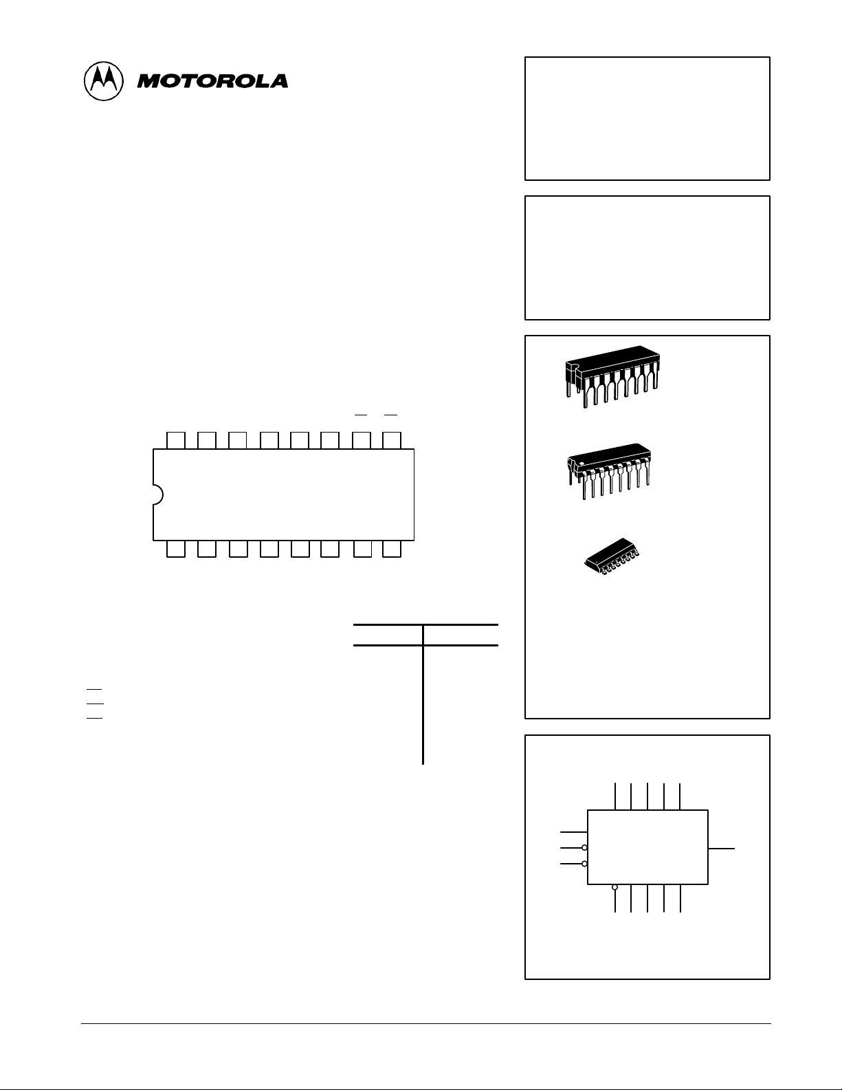
CONNECTION DIAGRAM DIP (TOP VIEW)
O0O1O2O
V
CC
16 15
3
14 13 12 11 10 9
CPQ
3
OE
SN74LS395
4-BIT SHIFT REGISTER
WITH 3-STATE OUTPUTS
LOW POWER SCHOTTKY
J SUFFIX
CERAMIC
16
1
16
1
CASE 620-09
N SUFFIX
PLASTIC
CASE 648-08
123456
DS P0P1P2P
MR
PIN NAMES LOADING (Note a)
P0–P
D
S
S
CP
MR
OE
O0–O
Q
3
NOTES:
a) 1 TTL Unit Load (U.L.) = 40 µA HIGH/1.6 mA LOW.
Parallel Inputs
3
Serial Data Input
Mode Select Input
Clock (Active LOW) Input
Master Reset (Active LOW) Input
Output Enable (Active HIGH) Input
3-State Register Outputs
3
Register Output
3
8
7
S GND
HIGH
0.5 U.L.
0.5 U.L.
0.5 U.L.
0.5 U.L.
0.5 U.L.
0.5 U.L.
65 U.L.
10 U.L.
LOW
0.25 U.L.
0.25 U.L.
0.25 U.L.
0.25 U.L.
0.25 U.L.
0.25 U.L.
15 U.L.
5 U.L.
16
1
ORDERING INFORMATION
SN74LSXXXJ Ceramic
SN74LSXXXN Plastic
SN74LSXXXD SOIC
LOGIC SYMBOL
3456
7
SP0P1P2P
2
D
10
9
S
CP
OE
MR O0O1O2O
15 14 13 12
1
VCC = PIN 16
GND = PIN 8
D SUFFIX
SOIC
CASE 751B-03
3
Q
3
3
11
FAST AND LS TTL DAT A
5-1
Page 2
LOGIC DIAGRAM
SN74LS395
P
S
D
CP
MR
OE
s
CP D
CD
O
0
0
CP D
Q
CD
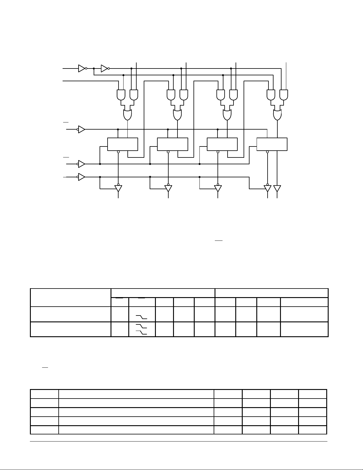
FUNCTION DESCRIPTION
The SN74LS395 contains four D-type edge-triggered
flip-flops and auxiliary gating to select a D input either from a
Parallel (Pn) input or from the preceding stage. When the
Select input is HIGH, the Pn inputs are enabled. A LOW signal
on the S input enables the serial inputs for shift-right operations, as indicated in the Truth Table.
State changes are initiated by HIGH-to-LOW transitions on
the Clock Pulse (CP) input. Signals on the Pn, Ds and S inputs
can change when the Clock is in either state, provided that the
recommended set-up and hold times are observed. When the
P
1
CP D
Q
O
1
CD
O
P
2
CP D
Q
2
CD
O3Q
P
3
Q
3
S input is LOW, a CP HIGH-LOW transition transfers data in
Q0 to Q1, Q1 to Q2, and Q2 to Q3. A left-shift is accomplished
by connecting the outputs back to the Pn inputs, but offset one
place to the left, i.e., O3 to P2, O2 to P1 and O1 to P0, with P
acting as the linking input from another package.
When the OE
input is HIGH, the output buffers are disabled
and the Q0–Q3 outputs are in a high impedance condition.
The shifting, parallel loading or resetting operations can still be
accomplished, however.
3
MODE SELECT — TRUTH TABLE
Inputs @ t
Operating Mode MR CP S D
Asynchronous Reset L X X X X L L L L
Shift, SET First Stage H L H X H O
Shift, RESET First Stage H L L X L O
Parallel Load H H X P
H = HIGH Voltage Level
L = LOW Voltage Level
X = Immaterial
tn, n + 1 = time before and after CP HIGH-to-LOW transition
NOTE:
When OE
is HIGH, outputs O0–O3 are in the high impedance state; however, this does not affect other operations or the Q3 output.
n
P
s
O
n
n
0
P
0
O
1
0n
0n
P
1
Outputs @ t
O
2
O
1n
O
1n
P
2
n+1
O
O
O
P
GUARANTEED OPERATING RANGES
Symbol Parameter Min Typ Max Unit
V
T
I
OH
I
OL
CC
A
Supply Voltage 4.75 5.0 5.25 V
Operating Ambient Temperature Range 0 25 70 °C
Output Current — High –0.4 mA
Output Current — Low 8.0 mA
FAST AND LS TTL DATA
5-2
3
2n
2n
3
Page 3
SN74LS395
VOLOutput LOW Volt
V
V
V
IIHI
HIGH C
t
I
V
5.0 V
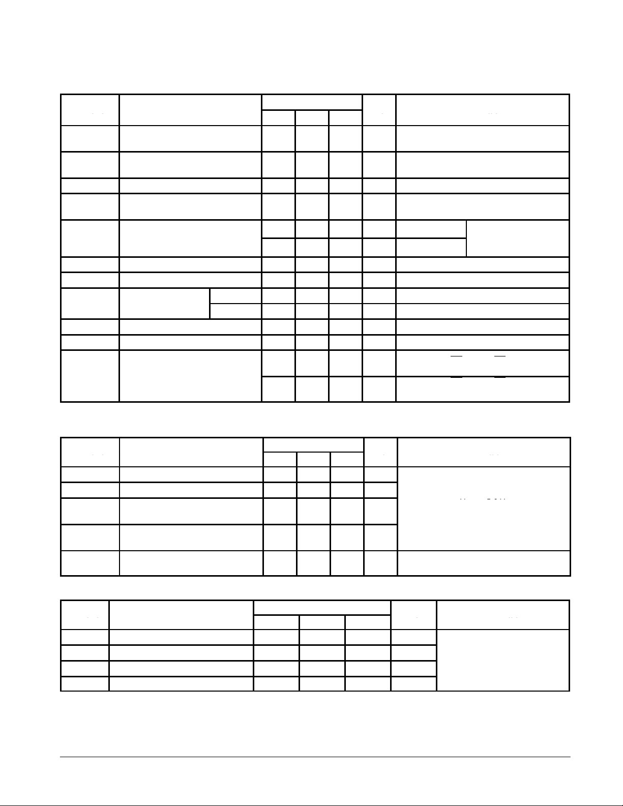
DC CHARACTERISTICS OVER OPERATING TEMPERATURE RANGE (unless otherwise specified)
Limits
Symbol Parameter
V
IH
V
IL
V
IK
V
OH
I
OZH
I
OZL
I
IL
I
OS
CC
Note 1: Not more than one output should be shorted at a time, nor for more than 1 second.
Input HIGH Voltage 2.0 V
Input LOW Voltage 0.8 V
Input Clamp Diode Voltage –0.65 –1.5 V VCC = MIN, IIN = –18 mA
Output HIGH Voltage 2.7 3.5 V
age
Output Off Current HIGH 20 µA VCC = MAX, VO = 2.4 V
Output Off Current LOW –20 µA VCC = MAX, VO = 0.4 V
nput
Input LOW Current –0.4 mA VCC = MAX, VIN = 0.4 V
Short Circuit Current (Note 1) –20 –100 mA VCC = MAX
Power Supply Current
Total, Output HIGH
Total, Output LOW 34 mA
urren
Min Typ Max
0.25 0.4 V IOL = 4.0 mA
0.35 0.5 V IOL = 8.0 mA
20 µA VCC = MAX, VIN = 2.7 V
–0.1 mA VCC = MAX, VIN = 7.0 V
31
Unit Test Conditions
Guaranteed Input HIGH Voltage for
All Inputs
Guaranteed Input LOW Voltage for
All Inputs
VCC = MIN, IOH = MAX, VIN = V
or VIL per Truth Table
mA VCC = MAX, OE = GND, CP = GND
VCC = MAX, OE = 4.5 V , CP
momentary 3.0 V then GND
IH
VCC = VCC MIN,
=
or
IN
IL
per Truth Table
IH
AC CHARACTERISTICS (T
Symbol Parameter
f
MAX
t
PHL
t
PLH
t
PHL
t
PZH
t
PZL
t
PLZ
t
PHZ
Maximum Input Clock Frequency 30 45 MHz
Propagation Delay, Clear to Output 22 35 ns
Propagation Delay, Low to High
Propagation Delay, High to Low
Output Enable Time
Output Disable Time
= 25°C)
A
AC SETUP REQUIREMENTS (T
Symbol Parameter
t
W
t
s
t
s
t
h
Clock Pulse Width 16 ns
Setup Time, Mode Select 40 ns
Setup Time, All Others 20 ns
Data Hold Time 10 ns
= 25°C)
A
Limits
Min Typ Max
15
25
15
17
12
11
Limits
Min Typ Max
30
30
25
25
20
17
Unit Test Conditions
ns
ns
ns CL = 5.0 pF
Unit Test Conditions
VCC = 5.0 V
CL = 15 pF
=
CC
FAST AND LS TTL DATA
5-3
Page 4
SN74LS395
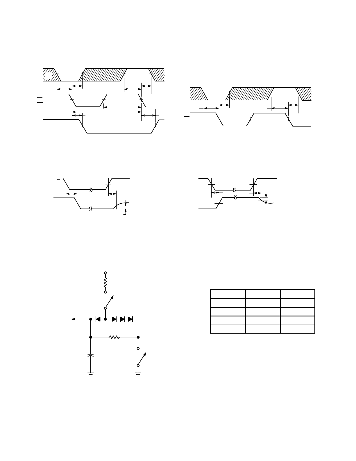
AC WAVEFORMS
The shaded areas indicate when the input is permitted to change for predictable output performance.
t
s(H)
1.3 V1.3 V
t
W
D
*
t
t
s(L)
CP OR
MR
Q
*The Data Input is DS for S = LOW and Pn for S = HIGH.
1.3 V
h(L)
t
PHL
1.3 V
1/f
max
Figure 1 Figure 2
V
V
E
OUT
1.3 V
t
PZL
1.3 V
1.3 V
0.5 V
t
PLZ
≈
1.3 V
V
OL
Figure 3
1.3 V
t
h(H)
t
PLH
LOAD SERIAL DATA
SHIFT RIGHT
S
t
s(L)
CP
E
V
1.3 V
OUT
V
t
PZH
1.3 V
LOAD PARALLEL DATA
t
h(L)
t
PHZ
t
s(H)
1.3V
≥
Figure 4
1.3 V1.3 V
V
OH
≈
1.3 V
0.5 V
1.3 V
t
h(H)
TO OUTPUT
UNDER TEST
V
CC
R
L
SW1
Ω
5 k
SW2CL*
* Includes Jig and Probe Capacitance.
AC LOAD CIRCUIT
Figure 5
SWITCH POSITIONS
SYMBOL SW1 SW2
t
PZH
t
PZL
t
PLZ
t
PHZ
Open Closed
Closed Open
Closed Closed
Closed Closed
FAST AND LS TTL DATA
5-4
 Loading...