

Page 1
SN54/74LS390
DUAL DECADE COUNTER;
DUAL 4-STAGE
BINARY COUNTER
The SN54/74LS390 and SN54/74LS393 each contain a pair of high-speed
4-stage ripple counters. Each half of the LS390 is partitioned into a
divide-by-two section and a divide-by five section, with a separate clock input
for each section. The two sections can be connected to count in the 8.4.2.1
BCD code or they can count in a biquinary sequence to provide a square wave
(50% duty cycle) at the final output.
Each half of the LS393 operates as a Modulo-16 binary divider, with the last
three stages triggered in a ripple fashion. In both the LS390 and the LS393,
the flip-flops are triggered by a HIGH-to-LOW transition of their CP inputs.
Each half of each circuit type has a Master Reset input which responds to a
HIGH signal by forcing all four outputs to the LOW state.
• Dual Versions of LS290 and LS293
• LS390 has Separate Clocks Allowing ÷2, ÷2.5, ÷5
• Individual Asynchronous Clear for Each Counter
• Typical Max Count Frequency of 50 MHz
• Input Clamp Diodes Minimize High Speed Termination Effects
SN54/74LS393
DUAL DECADE COUNTER;
DUAL 4-STAGE
BINARY COUNTER
LOW POWER SCHOTTKY
J SUFFIX
CERAMIC
16
1
16
1
CASE 620-09
N SUFFIX
PLASTIC
CASE 648-08
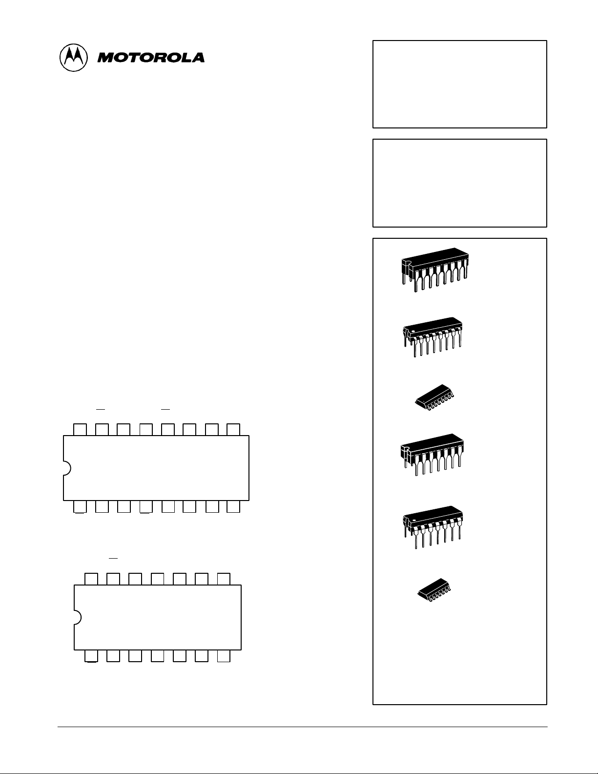
CONNECTION DIAGRAM DIP (TOP VIEW)
SN54/74LS390
V
CP
CC
16 15
123456
CP
0
MR Q0CP
0
14 13 12 1 1 10 9
MR Q0CP
1
1Q1Q2Q3
Q
Q
1
SN54/74LS393
VCCCP
14 13 12 11 10 9
123456
CP
MR Q0Q1Q2Q
MR Q0Q1Q2Q3GND
Q
2
7
GND
3
8
7
3
8
NOTE:
The Flatpak version
has the same pinouts
(Connection Diagram) as
the Dual In-Line Package.
D SUFFIX
16
1
14
1
14
1
14
1
CASE 751B-03
J SUFFIX
CERAMIC
CASE 632-08
N SUFFIX
PLASTIC
CASE 646-06
D SUFFIX
CASE 751A-02
ORDERING INFORMATION
SN54LSXXXJ Ceramic
SN74LSXXXN Plastic
SN74LSXXXD SOIC
SOIC
SOIC
FAST AND LS TTL DAT A
5-1
Page 2
SN54/74LS390 • SN54/74LS393
PIN NAMES LOADING (Note a)
CP Clock (Active LOW going edge)
CP
0
CP
1
MR Master Reset (Active HIGH) Input 0.5 U.L. 0.25 U.L.
Q0–Q
NOTES:
a) 1 TTL Unit Load (U.L.) = 40 µA HIGH/1.6 mA LOW.
b) The Output LOW drive factor is 2.5 U.L. for Military (54) and 5 U.L. for Commercial (74)
b) T emperature Ranges.
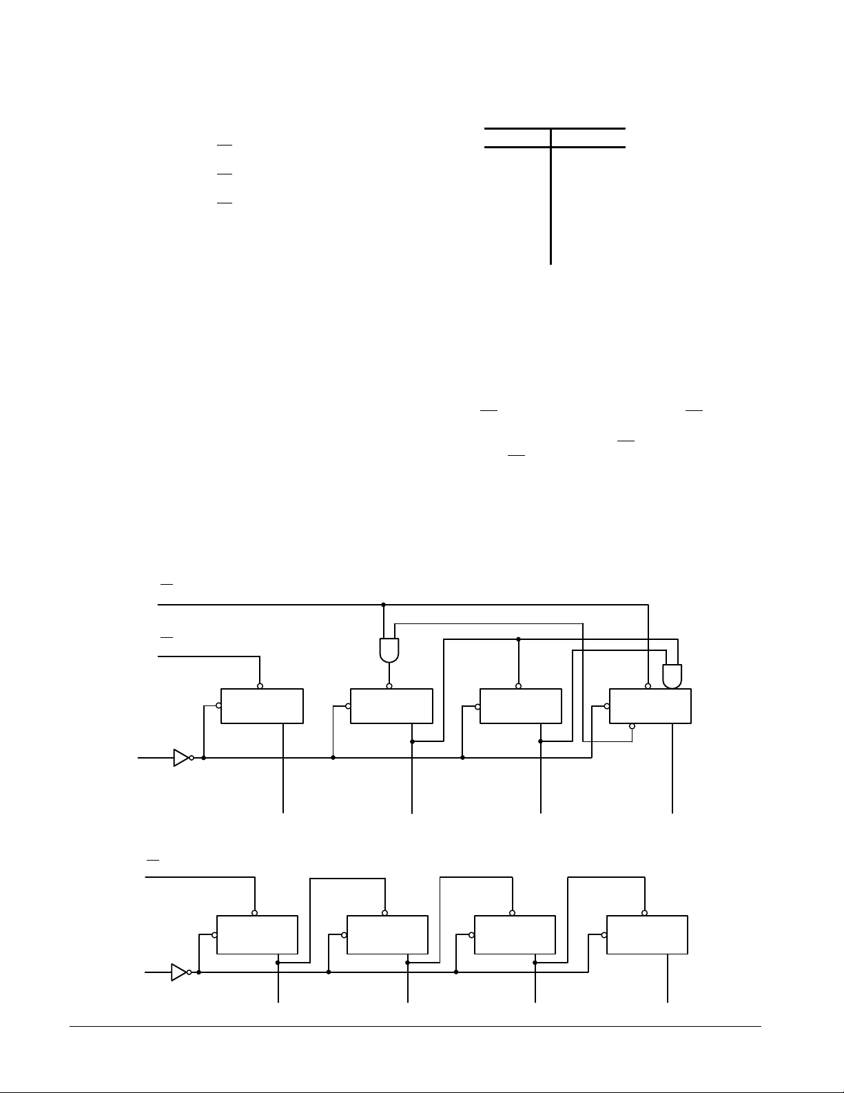
FUNCTIONAL DESCRIPTION
Each half of the SN54/74LS393 operates in the Modulo 16
binary sequence, as indicated in the ÷16 Truth T able. The first
flip-flop is triggered by HIGH-to-LOW transitions of the CP
input signal. Each of the other flip-flops is triggered by a
HIGH-to-LOW transition of the Q output of the preceding
flip-flop. Thus state changes of the Q outputs do not occur
simultaneously. This means that logic signals derived from
combinations of these outputs will be subject to decoding
spikes and, therefore, should not be used as clocks for other
counters, registers or flip-flops. A HIGH signal on MR forces
all outputs to the LOW state and prevents counting.
Each half of the LS390 contains a ÷5 section that is
independent except for the common MR function. The ÷ 5
Input to +16 (LS393) 0.5 U.L. 1.0 U.L.
Clock (Active LOW going edge)
Input to ÷2 (LS390) 0.5 U.L. 1.0 U.L.
Clock (Active LOW going edge)
Input to ÷5 (LS390) 0.5 U.L. 1.5 U.L.
Flip-Flop outputs (Note b) 10 U.L. 5 (2.5) U.L.
3
HIGH
LOW
section operates in 4.2.1 binary sequence, as shown in the ÷5
Truth Table, with the third stage output exhibiting a 20% duty
cycle when the input frequency is constant. To obtain a ÷10
function having a 50% duty cycle output, connect the input
signal to CP
and connect the Q3 output to the CP0 input; the
1
Q0 output provides the desired 50% duty cycle output. If the
input frequency is connected to CP
connected to CP
, a decade divider operating in the 8.4.2.1
1
and the Q0 output is
0
BCD code is obtained, as shown in the BCD Truth T able. Since
the flip-flops change state asynchronously, logic signals
derived from combinations of LS390 outputs are also subject
to decoding spikes. A HIGH signal on MR forces all outputs
LOW and prevents counting.
MR
CP
MR
CP
CP
SN54/74LS390 LOGIC DIAGRAM (one half shown)
1
0
KCP J
C
D
Q
Q
0
KCP J
C
D
Q
Q
1
KCP J
C
D
Q
Q
2
KCP
C
D
J
Q
Q
3
SN54/74LS393 LOGIC DIAGRAM (one half shown)
KCP J
C
D
Q
KCP J
C
D
Q
KCP J
C
D
Q
KCP J
C
D
Q
Q
0
Q
1
FAST AND LS TTL DATA
5-2
Q
2
Q
3
Page 3
SN54/74LS390 • SN54/74LS393
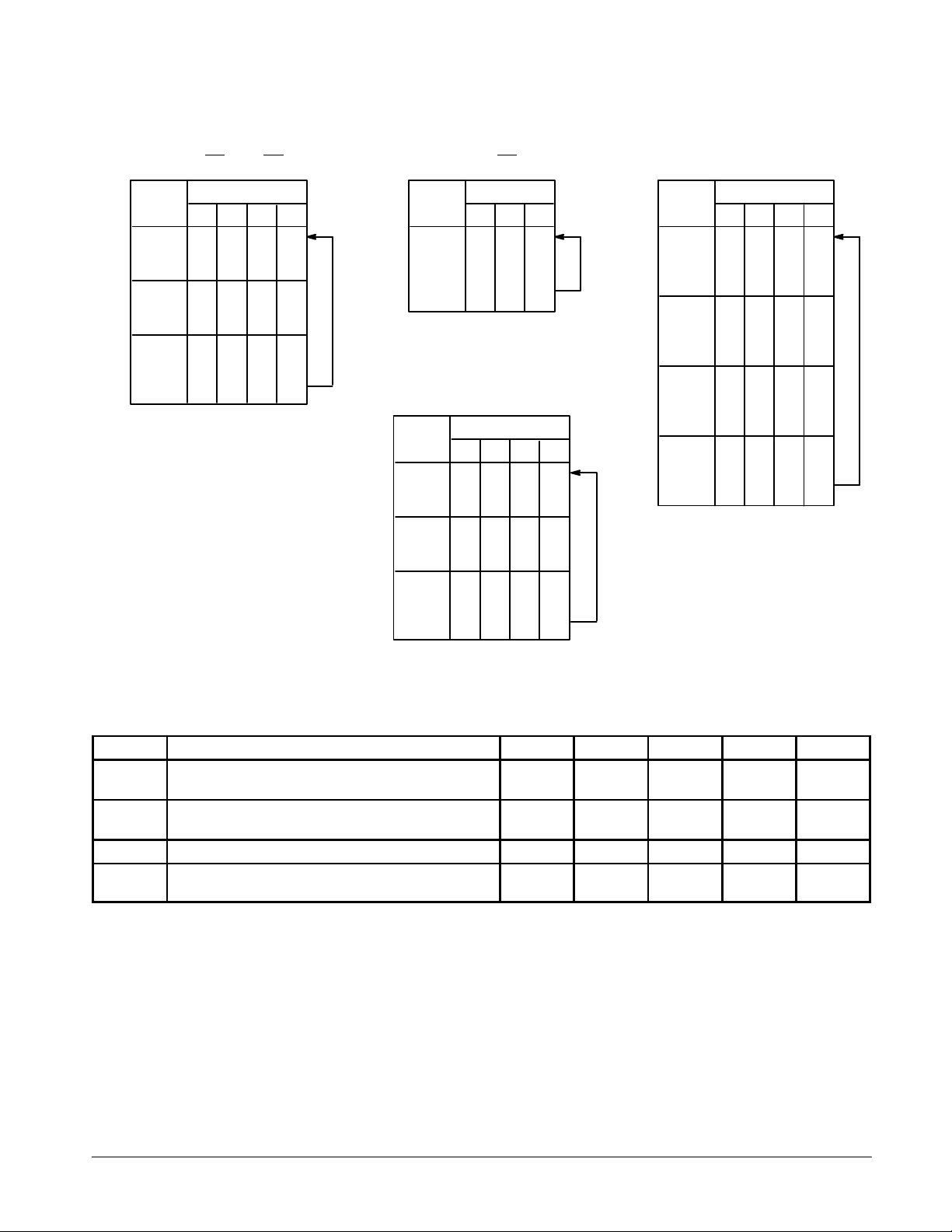
SN54/74LS390 BCD
TRUTH TABLE
(Input on CP
COUNT
0
1
2
3
4
5
6
7
8
9
; Q0 CP1)
0
OUTPUTS
Q3Q2Q1Q
L
L
L
L
L
L
L
L
L
H
L
H
L
H
L
H
H
L
H
L
SN54/74LS390 ÷5
TRUTH TABLE
SN54/74LS393
TRUTH TABLE
(Input on CP1)
0
L
L
L
H
H
L
H
H
L
L
L
H
H
L
H
H
L
L
L
H
COUNT
0
1
2
3
4
SN54/74LS390 ÷10 (50% @ Q0)
TRUTH TABLE
(Input on CP1, Q3 to CP0)
COUNT
0
1
2
3
4
5
6
7
8
9
OUTPUTS
Q3Q2Q
L
L
L
L
H
OUTPUTS
Q3Q2Q1Q
L
L
L
L
L
H
L
H
H
L
L
L
L
L
L
H
L
H
H
L
1
L
L
H
L
L
H
H
H
L
L
L
H
L
H
L
L
H
L
H
L
COUNT
0
1
2
3
4
5
6
7
8
9
10
11
0
L
L
L
L
L
H
H
H
H
H
12
13
14
15
H = HIGH Voltage Level
L = LOW Voltage Level
OUTPUTS
Q3Q2Q1Q
L
L
L
L
L
L
L
L
L
H
H
H
H
H
H
H
H
L
L
L
L
H
L
H
L
H
L
H
H
H
H
H
L
L
L
L
L
H
L
H
H
L
H
L
H
H
H
H
0
L
H
L
H
L
H
L
H
L
H
L
H
L
H
L
H
GUARANTEED OPERATING RANGES
Symbol Parameter Min Typ Max Unit
V
T
I
I
CC
A
OH
OL
Supply Voltage 54
74
Operating Ambient Temperature Range 54
74
Output Current — High 54, 74 –0.4 mA
Output Current — Low 54
74
4.5
4.75
–55
0
5.0
5.0
25
25
5.5
5.25
125
70
4.0
8.0
FAST AND LS TTL DATA
5-3
V
°C
mA
Page 4
SN54/74LS390 • SN54/74LS393
VILI
LOW Volt
V
pg
VOHOutput HIGH Volt
CC
,
OH
,
IN IH
VOLOutput LOW Volt
V
V
V
IIHI
HIGH C
t
L
p
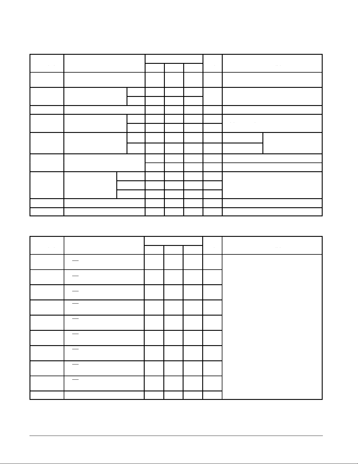
DC CHARACTERISTICS OVER OPERATING TEMPERATURE RANGE (unless otherwise specified)
Limits
Symbol Parameter
V
IH
V
IK
I
IL
I
OS
I
CC
Note 1: Not more than one output should be shorted at a time, nor for more than 1 second.
Input HIGH Voltage 2.0 V
nput
Input Clamp Diode Voltage –0.65 –1.5 V VCC = MIN, IIN = –18 mA
nput
Input LOW Current
Short Circuit Current (Note 1) –20 –100 mA VCC = MAX
Power Supply Current 26 mA VCC = MAX
age
urren
age
age
54, 74 0.25 0.4 V IOL = 4.0 mA
MR –0.4 mA
CP, CP
CP
1
Min Typ Max
54 0.7
74 0.8
54 2.5 3.5 V
74 2.7 3.5 V
74 0.35 0.5 V IOL = 8.0 mA
0.1 mA VCC = MAX, VIN = 7.0 V
0
–1.6 mA
–2.4 mA
Unit Test Conditions
Guaranteed Input HIGH Voltage for
All Inputs
Guaranteed Input LOW Voltage for
All Inputs
VCC = MIN, IOH = MAX, VIN = V
or VIL per Truth Table
20 µA VCC = MAX, VIN = 2.7 V
VCC = MAX, VIN = 0.4 V
IH
VCC = VCC MIN,
=
or
IN
IL
per Truth Table
IH
AC CHARACTERISTICS (T
Symbol Parameter
f
MAX
f
MAX
t
PLH
t
PHL
t
PLH
t
PHL
t
PLH
t
PHL
t
PLH
t
PHL
t
PLH
t
PHL
t
PLH
t
PHL
t
PLH
t
PHL
t
PHL
Maximum Clock Frequency
CP
to Q
0
0
Maximum Clock Frequency
CP
to Q
1
1
Propagation Delay,
CP
to Q
0
CP0 to Q
CP to Q
CP0 to Q
CP1 to Q
CP1 to Q
CP
MR to Any Output LS390/393 24 39 ns
1
to Q
0
3
2
1
2
3
= 25°C, VCC = 5.0 V)
A
LS393
LS390
LS393
LS390
LS390
LS390
LS390
Limits
Min Typ Max
25 35 MHz
20 MHz
12
13
12
13
40
40
37
39
13
14
24
26
13
14
20
20
20
20
60
60
60
60
21
21
39
39
21
21
Unit Test Conditions
ns
ns
ns
ns
ns
ns
ns
CL = 15 pF
FAST AND LS TTL DATA
5-4
Page 5
SN54/74LS390 • SN54/74LS393
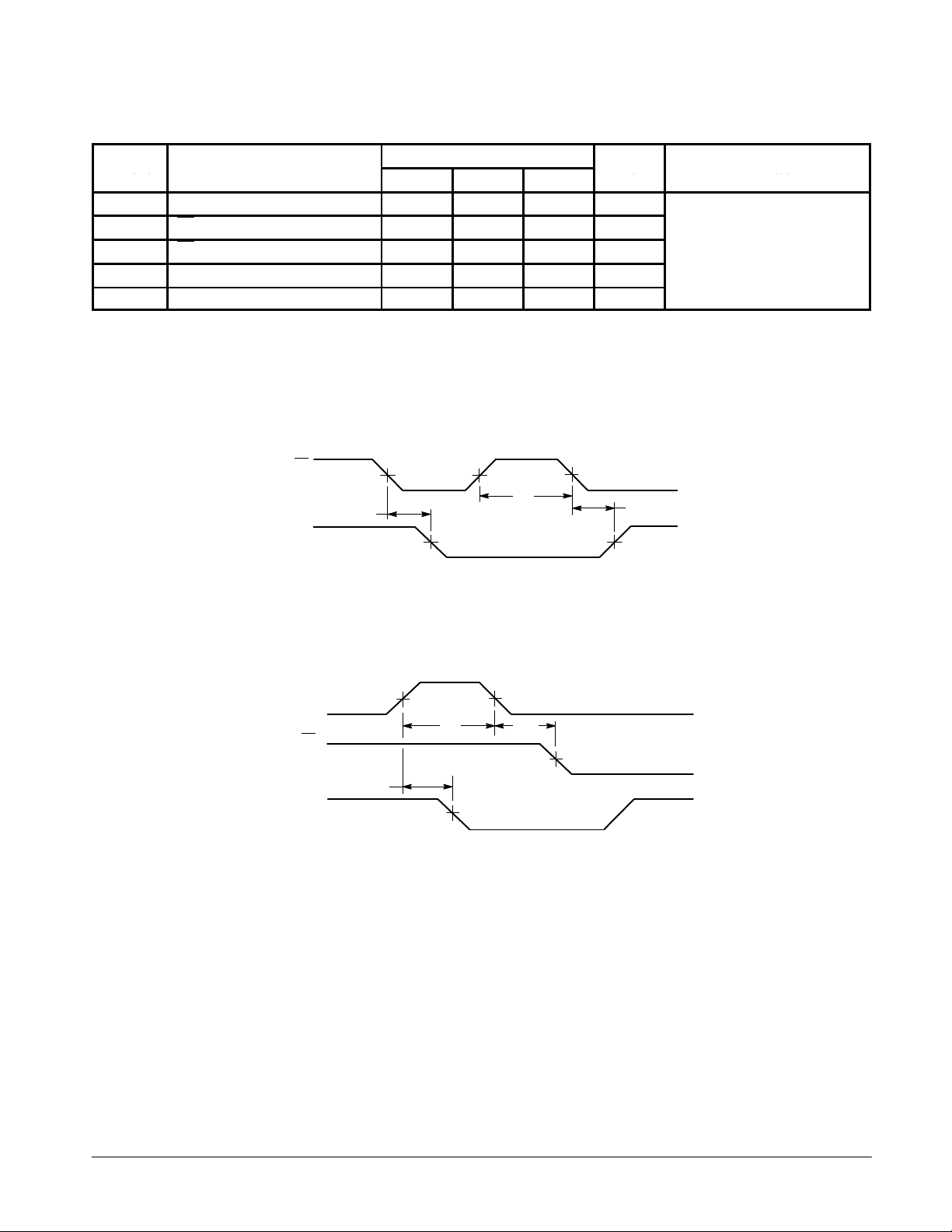
AC SETUP REQUIREMENTS (T
Symbol Parameter
t
t
t
t
t
W
W
W
W
rec
Clock Pulse Width LS393 20 ns
CP0 Pulse Width LS390 20 ns
CP
Pulse Width
1
MR Pulse Width LS390/393 20 ns
Recovery Time LS390/393 25 ns
= 25°C, VCC = 5.0 V)
A
Limits
Min Typ Max
LS390 40 ns
AC WAVEFORMS
*CP
Q
1.3 V
t
PHL
1.3 V
1.3 V
t
W
Figure 1
Unit Test Conditions
VCC = 5.0 V
t
PLH
1.3 V
MR & MS
1.3 V 1.3 V
CP
t
PHL
Q
*The number of Clock Pulses required between t
PHL
and t
t
W
1.3 V
t
rec
1.3 V
Figure 2
measurements can be determined from the appropriate Truth Table.
PLH
FAST AND LS TTL DATA
5-5
 Loading...