

Page 1
SN54/74LS377
SN54/74LS378
OCTAL D FLIP-FLOP WITH ENABLE;
HEX D FLIP-FLOP WITH ENABLE;
4-BIT D FLIP-FLOP WITH ENABLE
The SN54/74LS377 is an 8-bit register built using advanced Low Power
Schottky technology. This register consists of eight D-type flip-flops with a
buffered common clock and a buffered common clock enable.
The SN54 /74LS378 is a 6-Bit Register with a buffered common enable.
This device is similar to the SN54/74LS174, but with common Enable rather
than common Master Reset.
The SN54/74LS379 is a 4-Bit Register with buffered common Enable. This
device is similar to the SN54 / 74LS175 but features the common Enable
rather then common Master Reset.
• 8-Bit High Speed Parallel Registers
• Positive Edge-Triggered D-Type Flip Flops
• Fully Buffered Common Clock and Enable Inputs
• True and Complement Outputs
• Input Clamp Diodes Limit High Speed Termination Effects
PIN NAMES LOADING (Note a)
HIGH
E Enable (Active LOW) Input 0.5 U.L. 0.25 U.L.
D0–D
CP Clock (Active HIGH Going Edge) Input 0.5 U.L. 0.25 U.L.
Q0–Q
Q0–Q
NOTES:
a) 1 TTL Unit Load (U.L.) = 40 µA HIGH/1.6 mA LOW.
b) The Output LOW drive factor is 2.5 U.L. for Military (54) and 5 U.L. for Commercial
(74) T emperature Ranges.
Data Inputs 0.5 U.L. 0.25 U.L.
3
True Outputs (Note b) 10 U.L. 5 (2.5) U.L.
3
Complemented Outputs (Note b) 10 U.L. 5 (2.5) U.L.
3
LOW
SN54/74LS379
OCTAL D FLIP-FLOP WITH
ENABLE; HEX D FLIP-FLOP
WITH ENABLE; 4-BIT D FLIP-FLOP
WITH ENABLE
LOW POWER SCHOTTKY
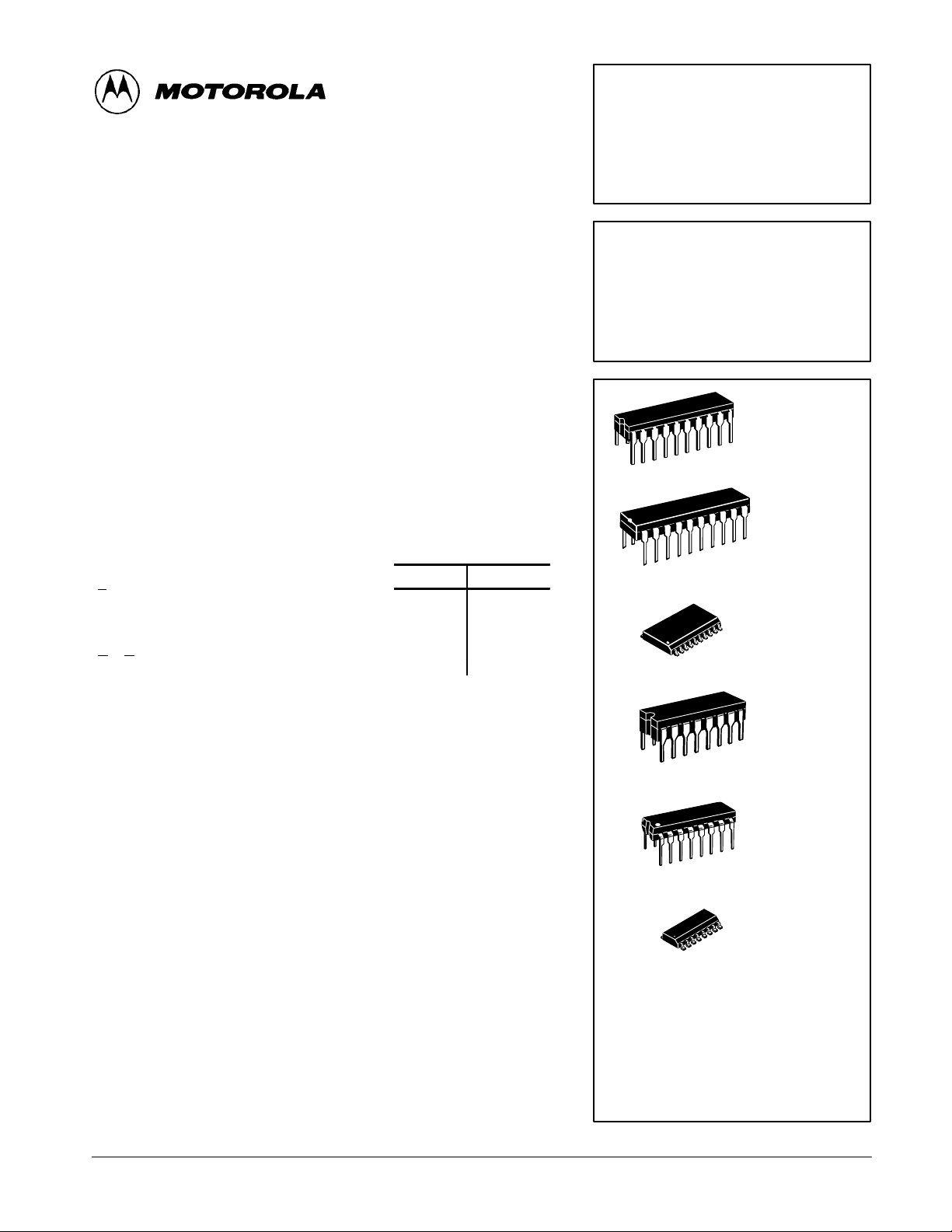
J SUFFIX
CERAMIC
20
1
20
1
20
1
16
1
CASE 732-03
N SUFFIX
PLASTIC
CASE 738-03
DW SUFFIX
SOIC
CASE 751D-03
J SUFFIX
CERAMIC
CASE 620-09
FAST AND LS TTL DAT A
5-1
N SUFFIX
16
1
16
1
CASE 648-08
D SUFFIX
CASE 751B-03
ORDERING INFORMATION
SN54LSXXXJ Ceramic
SN74LSXXXN Plastic
SN74LSXXXDW SOIC
SN74LSXXXD SOIC
PLASTIC
SOIC
Page 2
SN54/74LS377 • SN54/74LS378 • SN54/74LS379
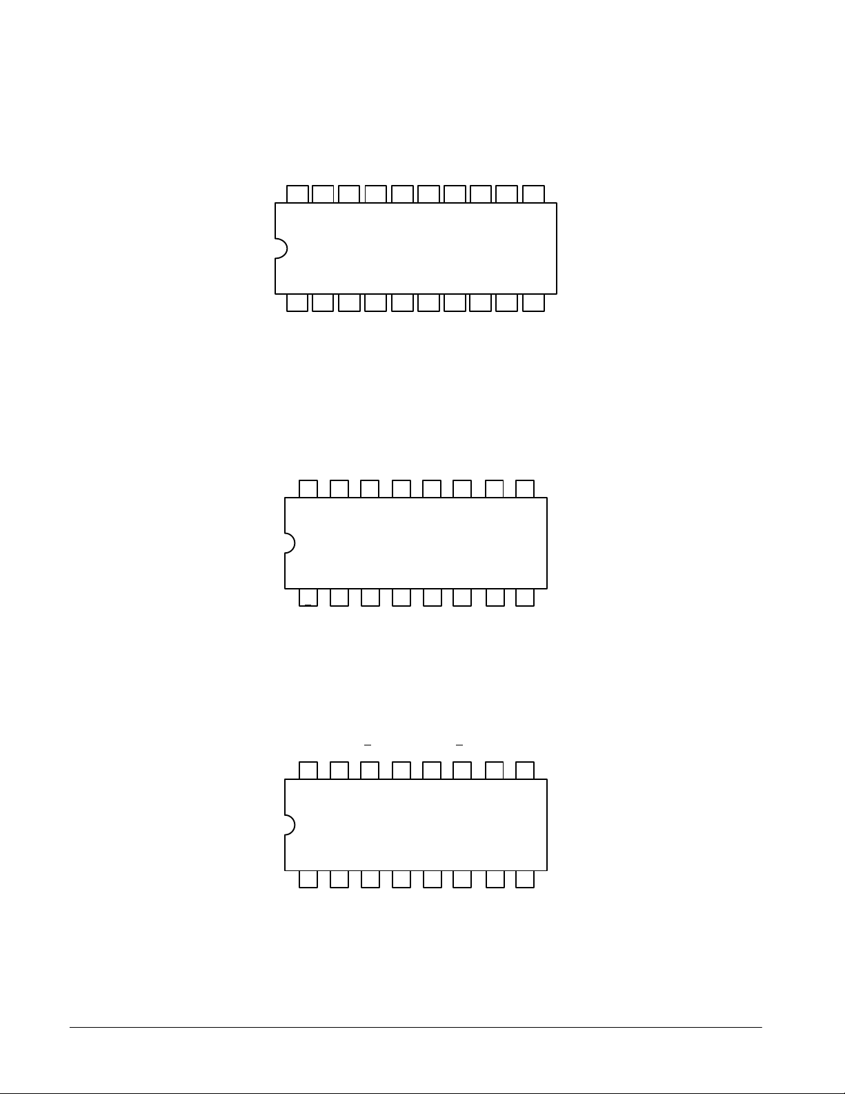
CONNECTION DIAGRAM DIPS (TOP VIEW)
SN54/74LS377
Q7D7D6Q
V
CC
20 19
18 17 16 15 14 13
Q
6
5
123456
Q0D0D1Q1Q2D2D
E
SN54/74LS378
Q5D5D4Q
V
CC
16 15
14 13 12 11 10 9
4
D
5
7
D
Q4CP
D
4
12 11
NOTE:
The Flatpak version
has the same pinouts
(Connection Diagram) as
the Dual In-Line Package.
8
910
Q
GND
3
3
Q
CP
3
3
123456
Q0D0D1Q1D2Q2GND
E
SN54/74LS379
Q3Q
V
CC
16 15
3D3D2
14 13 12 11 10 9
123456
E
Q0Q
0D0D1Q1Q1
Q
2
7
Q
2
7
NOTE:
The Flatpak version
has the same pinouts
(Connection Diagram) as
the Dual In-Line Package.
8
CP
NOTE:
The Flatpak version
has the same pinouts
(Connection Diagram) as
the Dual In-Line Package.
8
GND
FAST AND LS TTL DATA
5-2
Page 3
SN54/74LS377 • SN54/74LS378 • SN54/74LS379
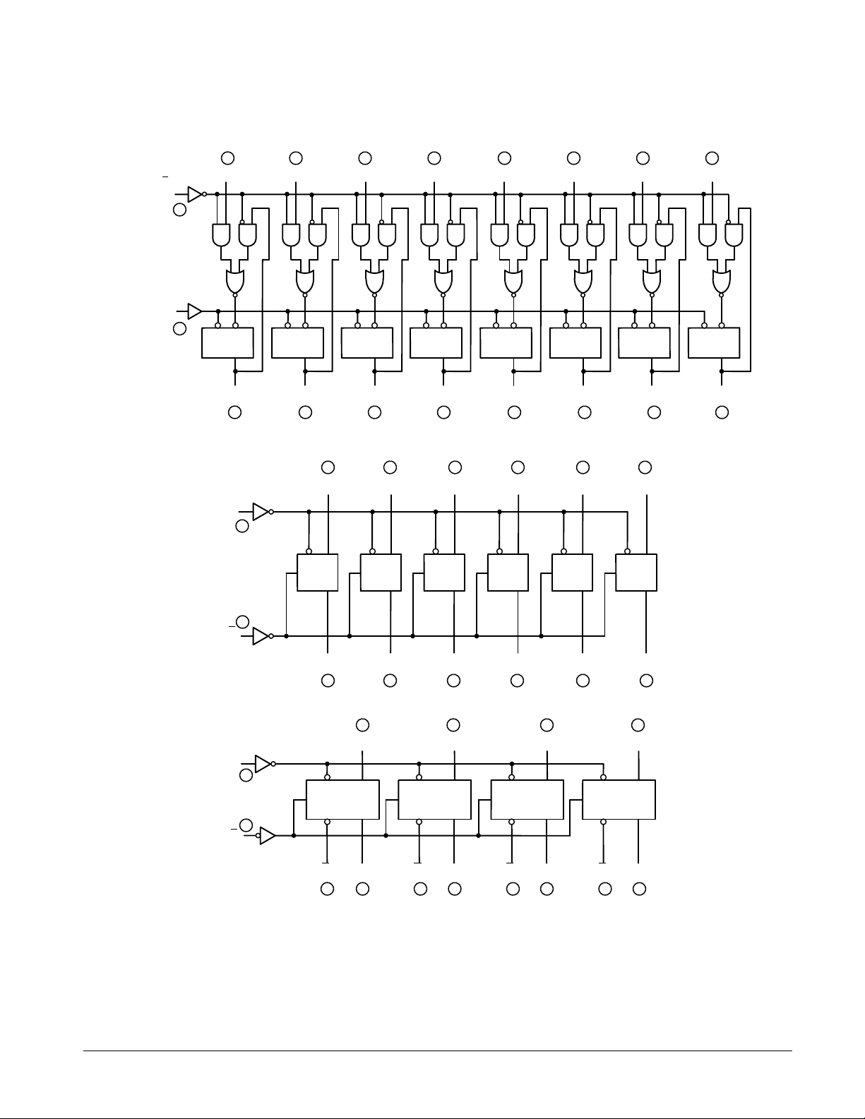
LOGIC DIAGRAMS
SN54/74LS377
E
ENABLE
CP
CLOCK
SN54/74LS378
3 84
D
0
1
11
CP D
Q
Q
0
26
D
1
CP D
Q
Q
1
5912 16
7
D
2
CP D
Q
Q
2
3 4
D
0
D
D
3
CP D
Q
Q
1
13 17
D
4
CP D
Q
3
6
D
2
Q
4
11
D
3
14
D
5
CP D
Q
Q
5
15 19
13
D
4
D
6
CP D
14
D
Q
Q
6
5
18
D
7
CP D
Q
Q
7
CP
9
SN54/74LS379
1
E
CP
9
1
E
CP D
E
Q
Q
0
2
CP D
E
Q
Q
0
3
CP D
E
Q
Q
4 5
D
0
Q
Q
0
267
1
5
CP D
E
Q
Q1Q
CP D
E
CP D
E
Q
Q
2
7
D
1
E
Q
1
Q
Q
3
10
CP D
Q
Q2Q
111210
D
Q
CP D
E
2
2
Q
Q
4
12
E
CP D
E
D
CP D
Q
Q3Q
14
Q
Q
5
15
13
3
Q
3
15
FAST AND LS TTL DATA
5-3
Page 4
SN54/74LS377 • SN54/74LS378 • SN54/74LS379
VILI
LOW Volt
V
Guaranteed Input LOW Voltage for
VOHOutput HIGH Volt
VCC MIN, IOH MAX, VIN V
IH
VOLOutput LOW Volt
V
V
V
IIHI
HIGH C
t
V
V
t
Enable Setup
CC
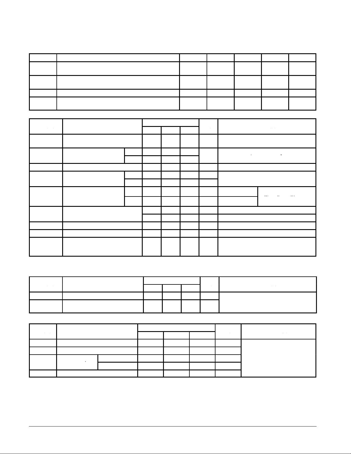
GUARANTEED OPERATING RANGES
Symbol Parameter Min Typ Max Unit
V
CC
T
A
I
OH
I
OL
DC CHARACTERISTICS OVER OPERATING TEMPERATURE RANGE (unless otherwise specified)
Symbol Parameter
V
IH
V
IK
I
IL
I
OS
I
CC
NOTE: With all inputs open and GND applied to all data and enable inputs, ICC is measured after a momentary GND, then 4.5 V is applied to clock.
Note 1: Not more than one output should be shorted at a time, nor for more than 1 second.
AC CHARACTERISTICS (T
Symbol Parameter
f
MAX
t
PLH
t
PHL
AC SETUP REQUIREMENTS (T
Symbol Parameter
t
W
t
s
s
t
h
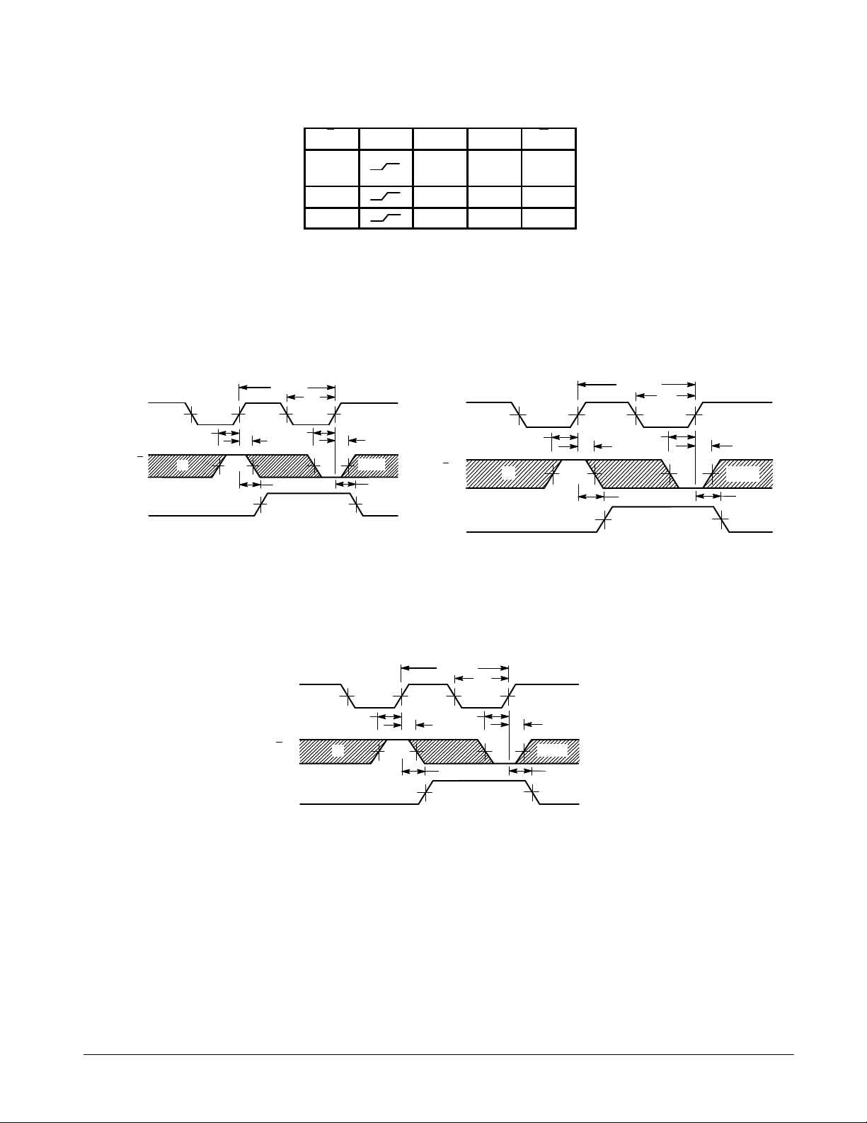
DEFINITION OF TERMS
SETUP TIME (ts) — is defined as the minimum time required
for the correct logic level to be present at the logic input prior to
the clock transition from LOW-to-HIGH in order to be recognized and transferred to the outputs.
HOLD TIME (th) — is defined as the minimum time following
Supply Voltage 54
Operating Ambient Temperature Range 54
Output Current — High 54, 74 –0.4 mA
Output Current — Low 54
Limits
Min Typ Max
Input HIGH Voltage 2.0 V
nput
Input Clamp Diode Voltage –0.65 –1.5 V VCC = MIN, IIN = –18 mA
nput
Input LOW Current –0.4 mA VCC = MAX, VIN = 0.4 V
Short Circuit Current (Note 1) –20 –100 mA VCC = MAX
Power Supply Current
Maximum Clock Frequency 30 40 MHz
Propagation Delay,
Clock to Output
Any Pulse Width 20 ns
Data Setup Time 20 ns
Enable Setup
Time
Any Hold Time 5.0 ns
age
age
age
urren
= 25°C, VCC = 5.0 V)
A
= 25°C, VCC = 5.0 V)
A
Inactive — State 10 ns
Active — State 25 ns
54 0.7
74 0.8
54 2.5 3.5 V
74 2.7 3.5 V
54, 74 0.25 0.4 V IOL = 4.0 mA
74 0.35 0.5 V IOL = 8.0 mA
LS377
LS378
LS379
Limits
Min Typ Max
17
18
Limits
Min Typ Max
74
74
74
20 µA VCC = MAX, VIN = 2.7 V
0.1 mA VCC = MAX, VIN = 7.0 V
28
22
15
27
27
4.5
4.75
–55
0
Unit Test Conditions
Guaranteed Input HIGH Voltage for
All Inputs
Guaranteed Input LOW Voltage for
All Inputs
VCC = MIN, IOH = MAX, VIN = V
or VIL per Truth Table
mA VCC = MAX, NOTE 1
Unit Test Conditions
ns
Unit Test Conditions
5.0
5.0
25
25
5.5
5.25
125
70
4.0
8.0
VCC = VCC MIN,
=
IN
IL
per Truth Table
= 5.0
CC
CL = 15 pF
VCC = 5.0 V
or
IH
IH
the clock transition from LOW-to-HIGH that the logic level
must be maintained at the input in order to ensure continued
recognition. A negative HOLD TIME indicates that the correct
logic level may be released prior to the clock transition from
LOW-to-HIGH and still be recognized.
V
°C
mA
FAST AND LS TTL DATA
5-4
Page 5
CP
D OR E
Q
SN54/74LS377 • SN54/74LS378 • SN54/74LS379
TRUTH TABLE
E CP D
H X No
L H H L
L L L H
L = LOW Voltage Level
H = HIGH Voltage Level
X = Immaterial
n
AC WAVEFORMS
SN54/74LS377 SN54/74LS378
1/f
max
t
1.3 V
t
s(H)
*
1.3 V
W
1.3 V
t
s(L)
t
h(H)
t
PLH
1.3 V 1.3 V
t
h(L)
1.3 V
t
PHL
Q
n
ChangeNoChange
CP
E
, D
Q
Q
n
1.3 V
t
s(H)
*
1.3 V
1/f
max
t
W
1.3 V
t
s(L)
t
h(H)
t
PHL
1.3 V 1.3 V
t
h(L)
1.3 V
t
PLH
Figure 1. Clock to Output Delays Clock Pulse
Width, Frequency, Setup and Hold Times Data
or Enable to Clock
CP
E
, D
Q
*The shaded areas indicate when the input is permitted to change for predictable output performance.
1.3 V
t
s(H)
*
Figure 3. Clock to Output Delays Clock Pulse
Width, Frequency, Setup and Hold Times Data,
SN54/74LS379
1/f
max
t
s(L)
t
h(H)
1.3 V
t
PLH
1.3 V 1.3 V
Enable to Clock
Figure 2. Clock to Output Delays Clock Pulse
Width, Frequency, Setup and Hold Times Data
or Enable to Clock
t
W
1.3 V
t
h(L)
1.3 V
t
PHL
FAST AND LS TTL DATA
5-5
 Loading...