

Page 1
4-BIT D LATCH
ggg
negative-going transition
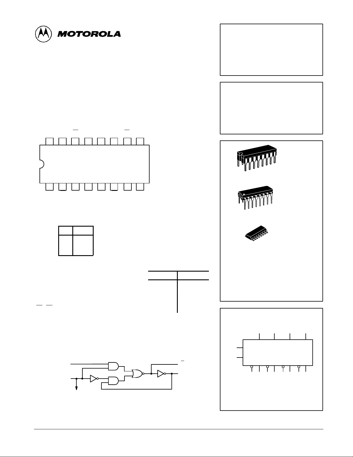
The SN54/74LS375 is a 4-Bit D-Type Latch for use as temporary storage
for binary information between processing limits and input/output or indicator
units. When the Enable (E) is HIGH, information present at the D input will be
transferred to the Q output and, if E is HIGH, the Q output will follow the input.
When E goes LOW, the information present at the D input prior to its setup time
will be retained at the Q outputs.
CONNECTION DIAGRAM DIP (TOP VIEW)
V
D3Q3Q3E
CC
16 15
2,3
14 13 12 11 10 9
Q
Q
2
D
2
2
NOTE:
The Flatpak version
has the same pinouts
(Connection Diagram) as
the Dual In-Line Package.
SN54/74LS375
4-BIT D LATCH
LOW POWER SCHOTTKY
J SUFFIX
CERAMIC
16
1
CASE 620-09
123456
D
Q
0
0Q0E0,1Q1Q1D1
7
GND
8
TRUTH TABLE
(Each latch)
t
t
n
n+1
D Q
H H
L L
PIN NAMES LOADING (Note a)
D1–D
E
0–1
E
2–3
Q1–Q
Q1–Q
NOTES:
a) 1 TTL Unit Load (U.L.) = 40 µA HIGH/1.6 mA LOW.
b) The Output LOW drive factor is 25 U.L. for Military (54) and 5 U.L. for Commercial (74)
T emperature Ranges.
Data Inputs
4
Enable Input Latches 0, 1 2.0 U.L. 1.0 U.L.
Enable Input Latches 2, 3 2.0 U.L. 1.0 U.L.
Latch Outputs (Note b) 10 U.L. 5 (2.5) U.L.
4
Complimentary Latch Outputs (Note b) 10 U.L. 5 (2.5) U.L.
4
NOTES:
tn = bit time before enable
negative-going transition.
t
= bit time after enable
n+1
ative-
oin
ne
transition.
HIGH
0.5 U.L. 0.25 U.L.
.
LOW
LOGIC DIAGRAM
DATA
ENABLE
Q
Q
16
1
16
1
CASE 648-08
CASE 751B-03
ORDERING INFORMATION
SN54LSXXXJ Ceramic
SN74LSXXXN Plastic
SN74LSXXXD SOIC
LOGIC SYMBOL
17 915
4
12
D0D
E
0,1
E
2,3
Q
0
2 3 6 5 10 11 14 13
1
Q
Q
1
N SUFFIX
PLASTIC
D SUFFIX
SOIC
D
2
Q
2
3
D
3
TO OTHER LA TCH
VCC = PIN 16
GND = PIN 8
FAST AND LS TTL DAT A
5-1
Page 2
SN54/74LS375
VILI
LOW Volt
V
pg
VOHOutput HIGH Volt
CC
,
OH
,
IN IH
VOLOutput LOW Volt
V
V
V
IIHI
HIGH C
t
CC
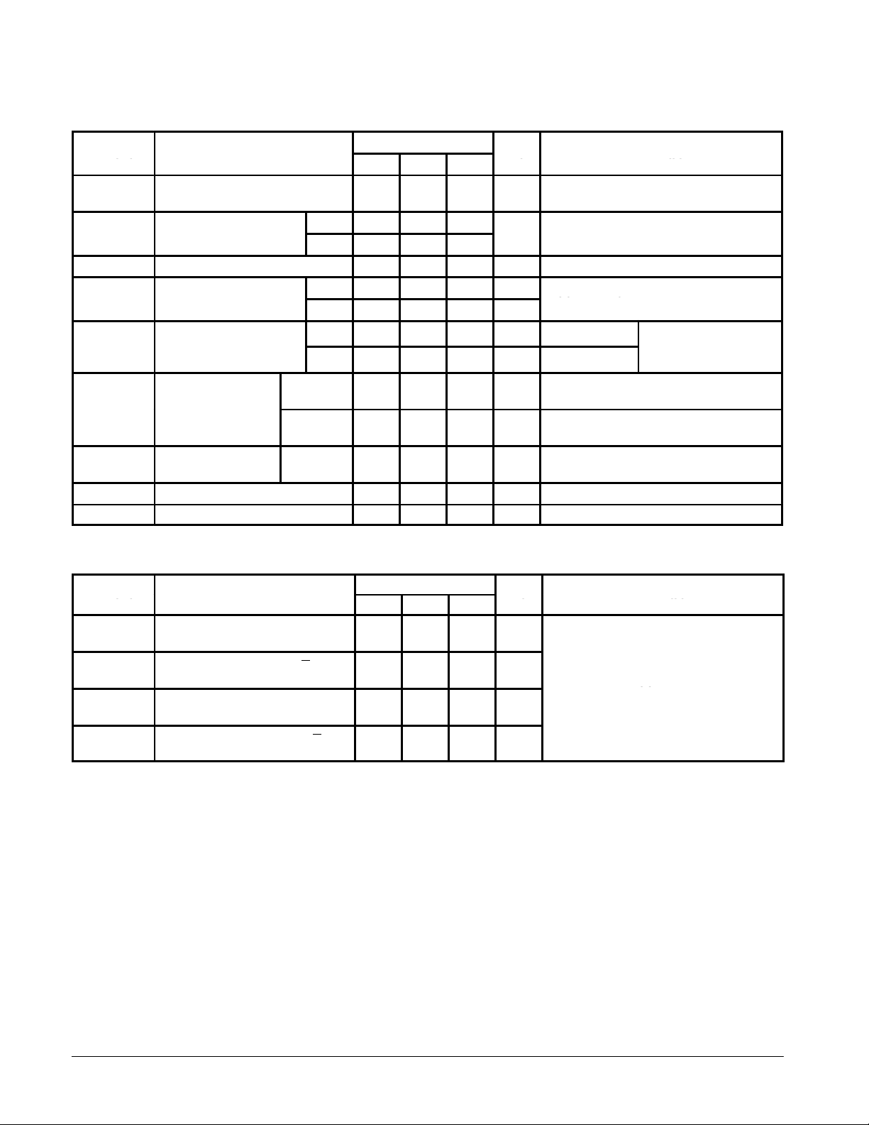
DC CHARACTERISTICS OVER OPERATING TEMPERATURE RANGE (unless otherwise specified)
Limits
Symbol Parameter
V
IH
V
IK
I
IL
I
OS
I
CC
Note 1: Not more than one output should be shorted at a time, nor for more than 1 second.
Input HIGH Voltage 2.0 V
nput
Input Clamp Diode Voltage –0.65 –1.5 V VCC = MIN, IIN = –18 mA
nput
Input LOW Current
Short Circuit Current (Note 1) –20 –100 mA VCC = MAX
Power Supply Current 12 mA VCC = MAX
age
age
age
urren
54 0.7
74 0.8
54 2.5 3.5 V
74 2.7 3.5 V
54, 74 0.25 0.4 V IOL = 4.0 mA
74 0.35 0.5 V IOL = 8.0 mA
D Input
E Input
D Input
E Input
D Input
E Input
Min Typ Max
20
80
0.1
0.4
–0.4
–1.6
Unit Test Conditions
Guaranteed Input HIGH Voltage for
All Inputs
Guaranteed Input LOW Voltage for
All Inputs
VCC = MIN, IOH = MAX, VIN = V
or VIL per Truth Table
µA VCC = MAX, VIN = 2.7 V
mA VCC = MAX, VIN = 7.0 V
mA VCC = MAX, VIN = 0.4 V
IH
VCC = VCC MIN,
=
or
IN
IL
per Truth Table
IH
AC CHARACTERISTICS (T
Symbol Parameter
t
PLH
t
PHL
t
PLH
t
PHL
t
PLH
t
PHL
t
PLH
t
PHL
Propagation Delay, Data to Q
Propagation Delay, Data to Q
Propagation Delay, Enable to Q
Propagation Delay, Enable to Q
A
= 25°C, VCC = 5.0 V)
Limits
Min Typ Max
15
9.0
12
7.0
15
14
16
7.0
27
17
20
15
27
25
30
15
Unit Test Conditions
ns
ns
ns
ns
VCC = 5.0 V
CL = 15 pF
FAST AND LS TTL DATA
5-2
Page 3
SN54/74LS375
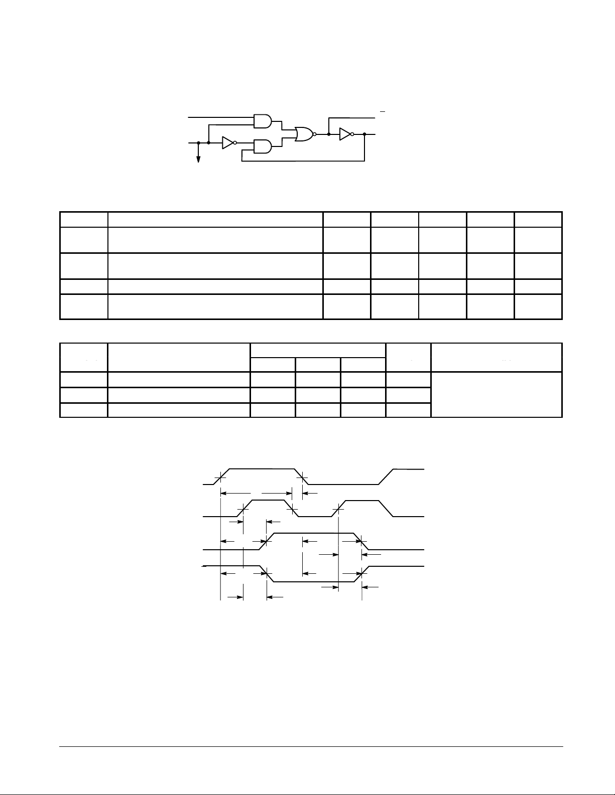
LOGIC DIAGRAM
DATA
ENABLE
TO OTHER LA TCH
Q (SN54LS/74LS375 ONLY)
Q
GUARANTEED OPERATING RANGES
Symbol Parameter Min Typ Max Unit
V
CC
T
A
I
OH
I
OL
AC SETUP REQUIREMENTS (T
Symbol Parameter
t
W
t
s
t
h
Supply Voltage 54
Operating Ambient Temperature Range 54
Output Current — High 54, 74 –0.4 mA
Output Current — Low 54
= 25°C, VCC = 5.0 V)
A
Limits
Min Typ Max
Enable Pulse Width 20 ns
Setup Time 20 ns
Hold Time 0 ns
74
74
74
4.5
4.75
–55
0
Unit Test Conditions
5.0
5.0
25
25
5.5
5.25
125
70
4.0
8.0
VCC = 5.0 V
V
°C
mA
AC WAVEFORMS
D
1.3 V 1.3 V
t
s
E
Q
Q
1.3 V 1.3 V 1.3 V
t
PLH
t
PHL
1.3 V
t
PLH
t
PHL
DEFINITION OF TERMS
SETUP TIME (ts) — is defined as the minimum time required
for the correct logic level to be present at the logic input prior to
the clock transition from LOW-to-HIGH in order to be recognized and transferred to the outputs.
HOLD TIME (th) — is defined as the minimum time following
t
h
t
PHL
t
PLH
t
PHL
t
PLH
1.3 V
1.3 V1.3 V
the clock transition from LOW-to-HIGH that the logic level
must be maintained at the input in order to ensure continued
recognition. A negative HOLD TIME indicates that the correct
logic level may be released prior to the clock transition from
LOW-to-HIGH and still be recognized.
FAST AND LS TTL DATA
5-3
 Loading...