

Page 1
DUAL 4-INPUT MULTIPLEXER
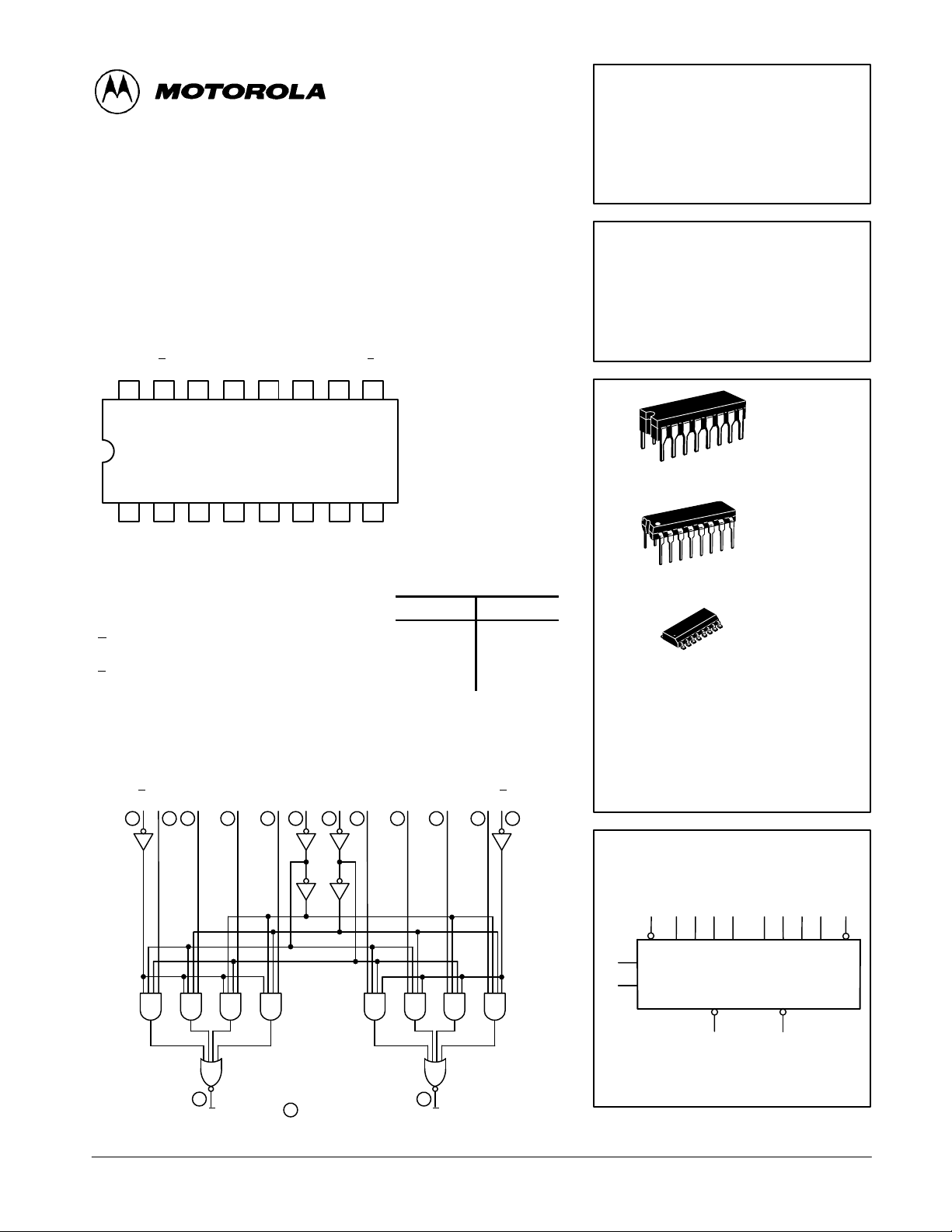
The SN54 / 74LS352 is a very high-speed Dual 4-input Multiplexer with
Common Select inputs and individual Enable inputs for each section. It can
select two bits of data from four sources. The two buffered outputs present
data in the inverted (complementary) form. The SN54/74LS352 is the functional equivalent of the SN54/74LS153 except with inverted outputs.
• Inverted Version of the SN54/74LS153
• Separate Enables for Each Multiplexer
• Input Clamp Diode Limit High Speed Termination Effects
CONNECTION DIAGRAM DIP (TOP VIEW)
V
EbS0I3bI
CC
16 15
2b
14 13 12 11 10 9
I
I
1b
0b
Z
b
NOTE:
The Flatpak version
has the same pinouts
(Connection Diagram) as
the Dual In-Line Package.
SN54/74LS352
DUAL 4-INPUT MULTIPLEXER
LOW POWER SCHOTTKY
J SUFFIX
CERAMIC
16
1
CASE 620-09
123456
E
S1I
a
PIN NAMES LOADING (Note a)
S0, S
1
E Enable (Active LOW) Input 0.5 U.L. 0.25 U.L.
I0–I
1
Z Multiplexer Outputs (note b) 10 U.L. 5 (2.5) U.L.
NOTES:
a) 1 TTL Unit Load (U.L.) = 40 µA HIGH/1.6 mA LOW.
b) The Output LOW drive factor is 2.5 U.L. for Military (54) and 5 U.L. for Commercial
(74) T emperature Ranges.
3aI2aI1aI0aZa
Common Select Inputs 0.5 U.L. 0.25 U.L.
Multiplexer Inputs 0.5 U.L. 0.25 U.L.
7
GND
8
HIGH
LOW
LOGIC DIAGRAM
I
E
0aI1aI2aI3aS1S0I0bI1bI2bI3b
a
345
14126
11 1210 13 15
E
b
16
1
16
1
ORDERING INFORMATION
SN54LSXXXJ Ceramic
SN74LSXXXN Plastic
SN74LSXXXD SOIC
LOGIC SYMBOL
16543 10111213
E
I
a
S
0
S
1
0aI1aI2aI3a
Z
a
14
2
N SUFFIX
PLASTIC
CASE 648-08
D SUFFIX
SOIC
CASE 751B-03
I0bI1bI2bI
3b
Z
b
15
E
b
VCC = PIN 16
7
Z
a
GND = PIN 8
= PIN NUMBERS
9
Z
b
FAST AND LS TTL DAT A
5-1
79
VCC = PIN 16
GND = PIN 8
Page 2
SN54/74LS352
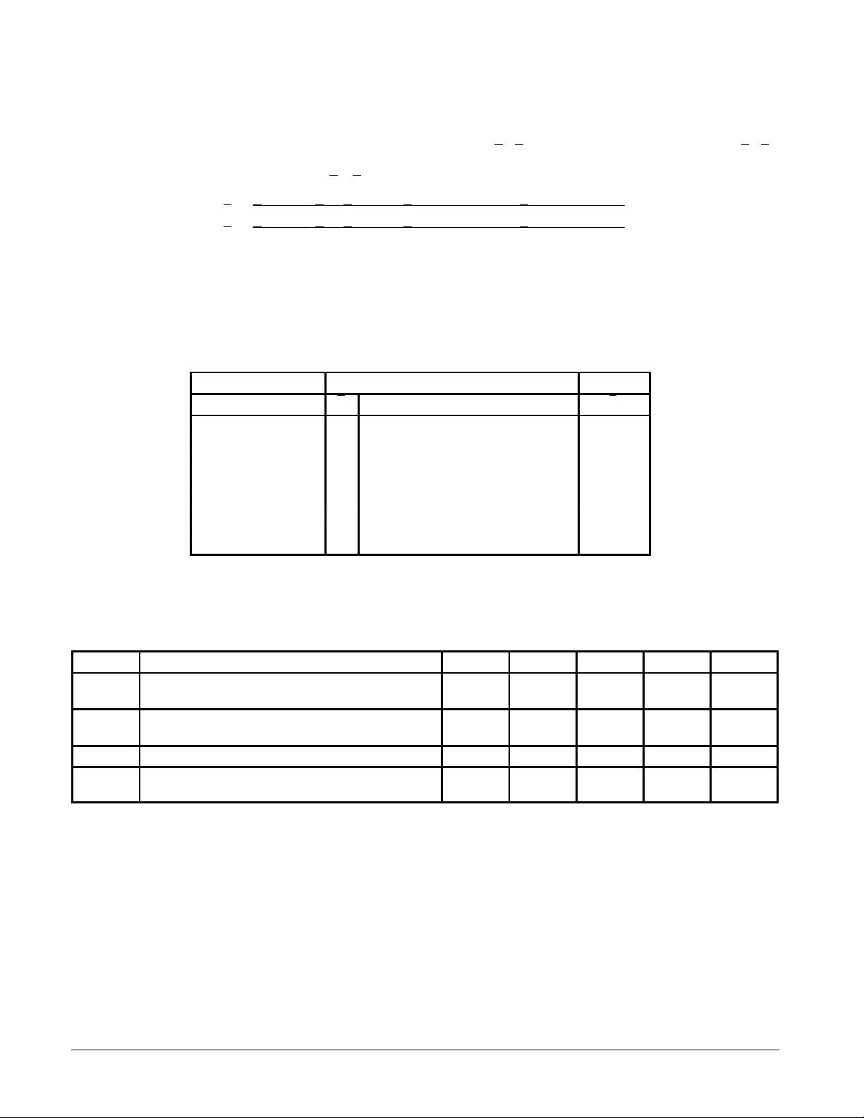
FUNCTIONAL DESCRIPTION
The SN54/74LS352 is a Dual 4-Input Multiplexer. It selects
two bits of data from up to four sources under the control of the
common Select Inputs (S0, S1). The two 4-input multiplexer
circuits have individual active LOW Enables (E
Z
= Ea • (I0a • S1 • S0 + I1a • S1 • S0 + I2a • S1 • S0 + I3a • S1 • S0)
a
= Eb • (I0b • S1 • S0 + I1b • S1 • S0 + I2b • S1 • S0 + I3b • S1 • S0)
Z
b
, Eb) which
a
can be used to strobe the outputs independently. When the
Enables (E
, Eb) are HIGH, the corresponding outputs (Za, Zb)
a
are forced HIGH.
The logic equations for the outputs are shown below.
The SN54/74LS352 can be used to move data from a group
of registers to a common output bus. The particular register
from which the data came would be determined by the state of
erator. The SN54/ 74LS352 can generate two functions of
three variables. This is useful for implementing highly irregular
random logic.
the Select Inputs. A less obvious application is a function gen-
TRUTH TABLE
SELECT INPUTS INPUTS (a or b) OUTPUT
S
0
X X H X X X X H
L LLLXXXH
L LLHXXXL
H LLXLXXH
H LLXHXXL
L HLXXLXH
L HLXXHXL
H HLXXXLH
H HLXXXHL
H = HIGH Voltage Level
L = LOW Voltage Level
X = Immaterial
S
1
E I
0
I
1
I
2
I
3
Z
GUARANTEED OPERATING RANGES
Symbol Parameter Min Typ Max Unit
V
T
I
OH
I
OL
CC
A
Supply Voltage 54
74
Operating Ambient Temperature Range 54
74
Output Current — High 54, 74 –0.4 mA
Output Current — Low 54
74
4.5
4.75
–55
0
5.0
5.0
25
25
5.5
5.25
125
70
4.0
8.0
V
°C
mA
FAST AND LS TTL DATA
5-2
Page 3
SN54/74LS352
VILI
LOW Volt
V
pg
VOHOutput HIGH Volt
CC
,
OH
,
IN IH
VOLOutput LOW Volt
V
V
V
IIHI
HIGH C
t
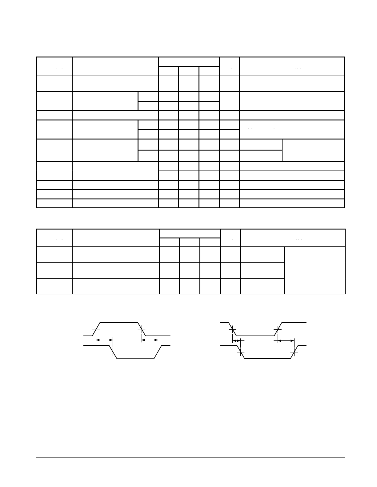
DC CHARACTERISTICS OVER OPERATING TEMPERATURE RANGE (unless otherwise specified)
Limits
Symbol Parameter
V
IH
V
IK
I
IL
I
OS
I
CC
Note 1: Not more than one output should be shorted at a time, nor for more than 1 second.
Input HIGH Voltage 2.0 V
nput
Input Clamp Diode Voltage –0.65 –1.5 V VCC = MIN, IIN = –18 mA
nput
Input LOW Current –0.4 mA VCC = MAX, VIN = 0.4 V
Short Circuit Current (Note 1) –20 –100 mA VCC = MAX
Power Supply Current 10 mA VCC = MAX
age
age
age
urren
54
74
54 2.5 3.5 V
74 2.7 3.5 V
54, 74 0.25 0.4 V IOL = 4.0 mA
74 0.35 0.5 V IOL = 8.0 mA
Min Typ Max
0.7
0.8
20 µA VCC = MAX, VIN = 2.7 V
0.1 mA VCC = MAX, VIN = 7.0 V
Unit Test Conditions
Guaranteed Input HIGH Voltage for
All Inputs
Guaranteed Input LOW Voltage for
All Inputs
VCC = MIN, IOH = MAX, VIN = V
or VIL per Truth Table
IH
VCC = VCC MIN,
=
or
IN
IL
per Truth Table
IH
AC CHARACTERISTICS (T
Symbol Parameter
t
PLH
t
PHL
t
PLH
t
PHL
t
PLH
t
PHL
Propagation Delay,
Select to Output
Propagation Delay,
Enable to Output
Propagation Delay,
Data to Output
V
IN
OUT
A
1.3 V 1.3 V
= 25°C, VCC = 5.0 V)
Limits
Min Typ Max
19
25
16
21
13
17
Unit Test Conditions
29
38
24
32
20
26
ns Figure 1 or 2
ns Figure 2
ns Figure 1
AC WAVEFORMS
t
PHL
1.3 V
t
PLH
1.3 VV
V
V
OUT
IN
1.3 V
t
PHL
1.3 V
t
PLH
Figure 1 Figure 2
VCC = 5.0 V,
CL = 15 pF
1.3 V
1.3 V
FAST AND LS TTL DATA
5-3
 Loading...