

Page 1
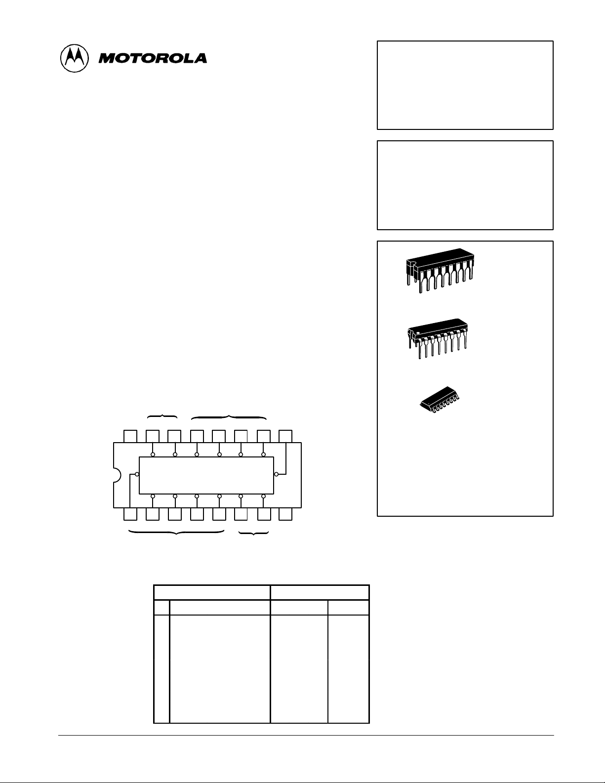
SN54/74LS348
8-INPUT PRIORITY ENCODERS
WITH 3-STATE OUTPUTS
The SN54/74LS348 and the SN54/74LS848 are eight input priority encod-
ers which provide the 8-line to 3-line function.
The outputs (A0–A2) and inputs (0–7) are active low. The active low input
which has the highest priority (input 7 has the highest) is represented on the
outputs (output A0 is the lowest bit). An example would be if inputs 1, 2 and 4
were low, then a binary 4 would be represented on the outputs.
The GS (Group Signal) output is active low when any of the inputs are low. It
serves to indicate when any of the inputs are active.
A0, A1 and A2 are three-state outputs. This allows for up to 64 line expansion without the need for special external circuitry .
A logical one on the Enable Input (EI) forces A0, A1 ared A2 to the disabled
state and outputs GS and EO to the high state. A high on all data inputs (0–7)
together with a low on the EI input disables outputs A0, A1, and A2 and forces
output GS to the high state and output EO to the low state.
Use of the EI input in conjunction with the EO output provides for the capability of having priority encoding of n input signals.
The LS848 has special internal circuitry providing for a greatly reduced negative going glitch on the GS (Group Signal) output and on a reduced tendency
for the A0, A1 and A2 outputs to become momentarily enabled. Both of these
occurrences happen when the EI input goes from a logical one to a logical zero
and all data inputs (0–7) are held at logical ones. The internal glitch reduction
circuitry does add an additional fan-in of one on all data inputs (compared to
that of the LS348).
OUTPUTS INPUTS
V
EO GS 3 2 01
CC
16 15
14 13 12 11 10 9
OUTPUT
A0
SN54/74LS848
8-INPUT PRIORITY ENCODERS
WITH 3-STATE OUTPUTS
LOW POWER SCHOTTKY
J SUFFIX
CERAMIC
16
1
16
1
16
1
CASE 620-09
N SUFFIX
PLASTIC
CASE 648-08
D SUFFIX
SOIC
CASE 751B-03
EO GS 3 2 01
4A0
567EIA2A1
123456
4
5 6 7 EI A2 A1 GND
OUTPUTSINPUTS
7
8
FUNCTION TABLE
INPUTS OUTPUTS
EI 0 1 2 3 4 5 6 7 A2 A1 A0 GS EO
H X X X X X X X X Z Z Z H H
L H HHHHHHH Z ZZH L
LXXXXXXXL L LLLH
LXXXXXXLH L LHLH
LXXXXXLHH L HLLH
LXXXXLHHH L HHL H
LXXXLHHHH H LLLH
LXXLHHHHH H LHLH
LXLHHHHHH H HLLH
LLHHHHHHHHHHLH
FAST AND LS TTL DAT A
5-1
ORDERING INFORMATION
SN54LSXXXJ Ceramic
SN74LSXXXN Plastic
SN74LSXXXD SOIC
H = HIGH Logic Level
L = LOW Logic Level
X = Irrelevant
Z = High Impedance State
Page 2
SN54/74LS348 • SN54/74LS848
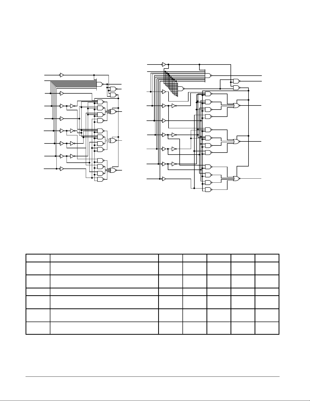
BLOCK DIAGRAMS
G1
G2
G3
G4
G5
G6
G7
G8
″
G13
G29
G9
G10
G11
G12
G31
G14
G15
′
′
′
′
G16
G17
G19
G20
G21
G22
G24
G25
G26
G27
′
′
′
′
′
′
′
G30
G18
G23
G28
(15)
(14)
(9)
(7)
(6)
EO
GS
A0
A1
A2
(5)
EI
(10)
(5)
EI
(10)
0
1
2
3
4
5
6
7
(11)
(12)
(13)
(1)
(2)
(3)
(4)
(15)
(14)
(9)
(7)
(6)
EO
GS
A0
A1
A2
0
1
2
3
4
5
6
7
(11)
(12)
(13)
(1)
(2)
(3)
(4)
SN54/74LS348 SN54/74LS848
GUARANTEED OPERATING RANGES
Symbol Parameter Min Typ Max Unit
V
T
I
OH
I
OH
I
OL
I
OL
CC
A
Supply Voltage 54
Operating Ambient Temperature Range 54
Output Current — High EO, GS 54, 74 –0.4 mA
Output Current — High A0, A1, A2
A0, A1, A2
Output Current — Low EO, GS 54
Output Current — Low A0, A1, A2
A0, A1, A2
74
74
54
74
74
54
74
4.5
4.75
–55
0
5.0
5.0
25
25
5.5
5.25
125
70
–1.0
–2.6
4.0
8.0
12
24
V
°C
mA
mA
mA
FAST AND LS TTL DATA
5-2
Page 3
SN54/74LS348 • SN54/74LS848
VILI
LOW Volt
V
pg
V
CC
MIN, I
OH
MAX, V
IN
V
IH
V
pg
V
V
V
V
pg
V
V
V
I
OS
,
CC
I
A
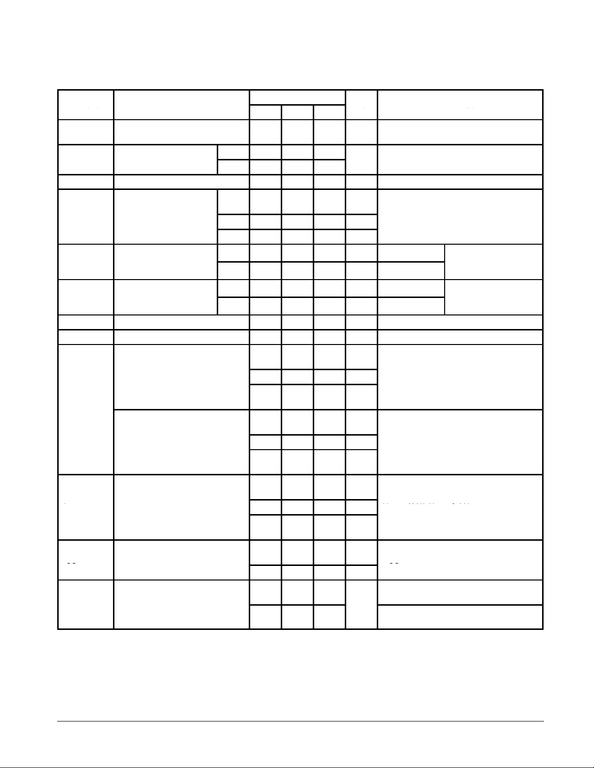
DC CHARACTERISTICS OVER OPERATING TEMPERATURE RANGE (unless otherwise specified)
Limits
Symbol Parameter
V
IH
V
IK
V
OH
OL
OL
I
OZH
I
OZL
IH
I
IL
Input HIGH Voltage 2.0 V
nput
Input Clamp Diode Voltage –0.65 –1.5 V VCC = MIN, IIN = –18 mA
Output HIGH Voltage
A0, A1, A2
EO, GS 54 2.5 3.5 V
EO, GS 74 2.7 3.5 V
Output LOW Voltage
EO, GS
Output LOW Voltage
A0, A1, A2
Output Off Current HIGH 20 µA VCC = MAX, V
Output Off Current LOW –20 µA VCC = MAX, V
Input HIGH Current
Input 0, EI — LS348 20 µA
Input 0 — LS848 40 µA
Other — LS348
Other — LS848
Input HIGH Current
Input 0, EI — LS348 0.1 mA
Input 0 — LS848 0.2 mA
Other — LS348
Other — LS848
Input LOW Current
Input 0, EI — LS348
Input 0 — LS848 –0.8 mA
Other — LS348
Other — LS848
age
54
74
54, 74 2.4 3.1 V
54, 74 0.25 0.4 V IOL = 4.0 mA
74 0.35 0.5 V IOL = 8.0 mA
54, 74 0.25 0.4 V IOL = 12 mA
74 0.35 0.5 V IOL = 24 mA
Min Typ Max
0.7
0.8
40
60
0.2
0.3
–0.4 mA
–0.8
–1.2mAmA
Unit Test Conditions
Guaranteed Input HIGH Voltage for
All Inputs
Guaranteed Input LOW Voltage for
All Inputs
V
= MIN I = MAX V = V
=
or VIL per Truth Table
VCC = MAX, VIN = 2.7 V
µA
µA
VCC = MAX, VIN = 7.0 V
mA
mA
VCC = MAX, VIN = 0.4 V
=
VCC = VCC MIN,
=
IN
per Truth Table
VCC = VCC MIN,
=
IN
per Truth Table
= 2.7 V
OUT
= 0.4 V
OUT
=
or
IL
IH
or
IL
IH
I
OS
CC
Note 1: Not more than one output should be shorted at a time, nor for more than 1 second.
Short Circuit Current (Note 1)
EO, GS
A0, A1, A2
Power Supply Current
Total, Output HIGH
Total, Output LOW 13 25
–20 –120 mA
–30 –130 mA
FAST AND LS TTL DATA
12 23
5-3
VCC = MAX
VCC = MAX
All Inputs and Outputs Open
m
VCC = MAX, Inputs 7, EI = GND
All Others Open
Page 4
SN54/74LS348 • SN54/74LS848
From
To
1 th
7
A0, A1
A2
1 th
7
A0, A1
A2
L
p
EI
A0, A1
A2
0 th
7
E0
0 th
7
GS
L
p
EI
GS
EI
EO
EI
A0, A1
A2
L
p
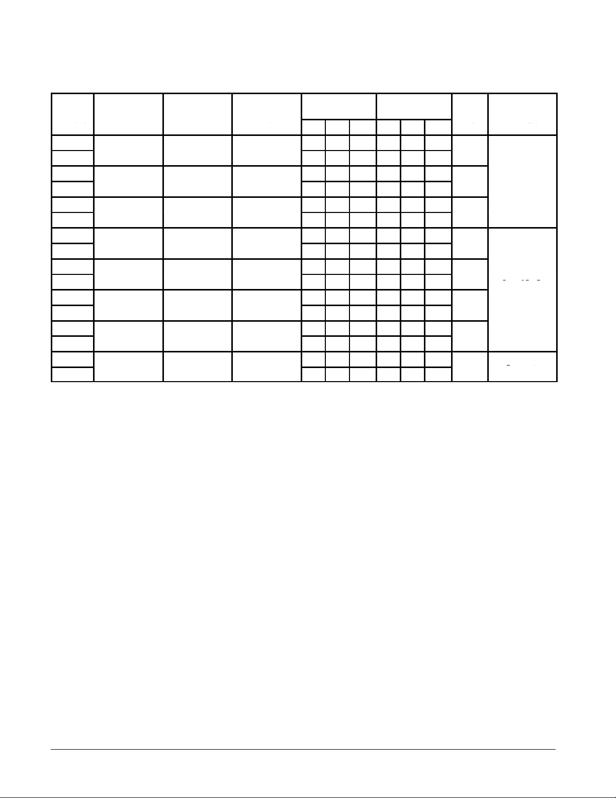
AC CHARACTERISTICS (V
From To
Symbol
t
PLH
t
PHL
t
PLH
t
PHL
t
PZH
t
PZL
t
PLH
t
PHL
t
PLH
t
PHL
t
PLH
t
PHL
t
PLH
t
PHL
t
PHZ
t
PLZ
(Input)
ru
ru
ru
ru
= 5.0 V, TA = 25°C)
CC
(Output)
or
or
or
or
LS348
Limits
Waveform
In-Phase 11 17 12 18
output 20 30 20 30
Out-of-Phase 23 35 23 35
output 23 35 23 35
Out-of-Phase 11 18 11 18
output 26 40 26 40
In-Phase 38 55 38 55
output 9.0 21 9.0 21
In-Phase 11 17 11 17
output 14 36 14 36
In-Phase 17 21 17 21
output 25 40 30 45
Min Typ Max Min Typ Max
25 39 25 39
24 41 24 41
18 27 18 27
23 35 23 35
LS848
Limits
Unit Test Conditions
ns
ns
ns
ns
ns
ns
ns
ns
CL = 45 pF
RL = 667 Ω
CL = 15 pF
RL = 2.0 Ω
CL = 5.0 pF
RL = 667 Ω
FAST AND LS TTL DATA
5-4
 Loading...