

Page 1
8-BIT SHIFT/STORAGE REGISTER
WITH 3-STATE OUTPUTS
The SN54/74LS323 is an 8-Bit Universal Shift/Storage Register with
3-state outputs. Its function is similar to the SN54/74LS299 with the exception
of Synchronous Reset. Parallel load inputs and flip-flop outputs are
multiplexed to minimize pin count. Separate inputs and outputs are provided
for flip-flops Q0 and Q7 to allow easy cascading.
Four operation modes are possible: hold (store), shift left, shift right, and
parallel load. All modes are activated on the LOW-to-HIGH transition of the
Clock.
• Common I/O for Reduced Pin Count
• Four Operation Modes: Shift Left, Shift Right, Parallel Load and Store
• Separate Continuous Inputs and Outputs from Q
Cascading
• Fully Synchronous Reset
• 3-State Outputs for Bus Oriented Applications
• Input Clamp Diodes Limit High-Speed Termination Effects
• ESD > 3500 Volts
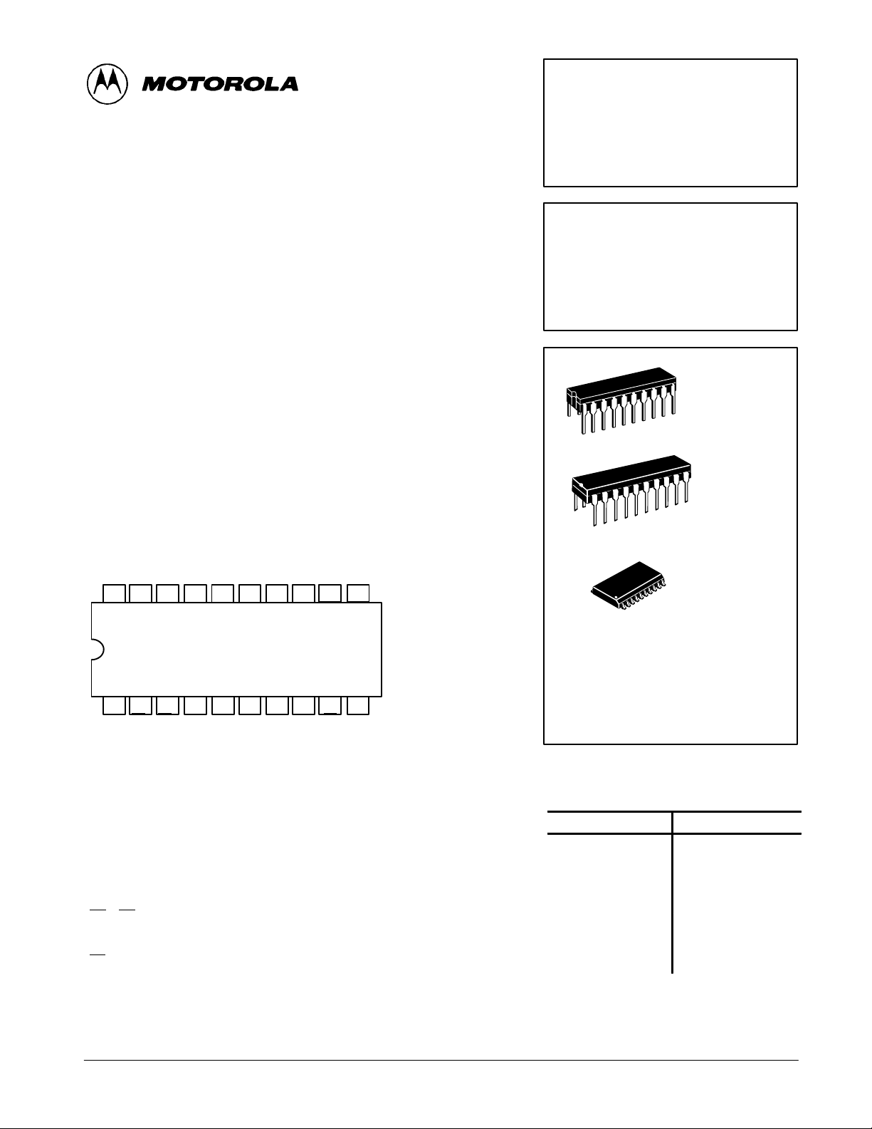
CONNECTION DIAGRAM DIP (TOP VIEW)
and Q7 Allow Easy
0
SN54/74LS323
8-BIT SHIFT/STORAGE REGISTER
WITH 3-STATE OUTPUTS
LOW POWER SCHOTTKY
J SUFFIX
CERAMIC
20
1
20
1
CASE 732-03
N SUFFIX
PLASTIC
CASE 738-03
V
S1DS7Q7I/O
CC
20 19
1234 56
S
0
PIN NAMES LOADING (Note a)
CP Clock Pulse (active positive going edge) Input 0.5 U.L. 0.25 U.L.
DS
0
DS
7
I/O
n
OE1, OE
Q0, Q
S0, S
1
SR Synchronous Reset (active LOW) Input 0.5 U.L. 0.25 U.L.
NOTES:
a) 1 TTL LOAD = 40 µA HIGH/1.6 mA LOW.
b) The output LOW drive factor is 2.5 U.L for Military (54) and 5 U.L. for Commercial Temperature Ranges.
c) The output LOW drive factor is 7.5 U.L for Military (54) and 15 U.L. for Commercial Temperature Ranges.
The output HIGH drive factor is 25 U.L. for Military (54) and 65 U.L. for Commercial Temperature Ranges.
18 17 16 15 14 13
OE
1OE2
2
7
7
I/O6I/O4I/O2I/O0Q
Serial Data Input for Right Shift 0.5 U.L. 0.25 U.L.
Serial Data Input for Left Shift 0.5 U.L. 0.25 U.L.
Parallel Data Input or
Parallel Output (3-State) (Note c)
3-State Output Enable (active LOW) Inputs 0.5 U.L. 0.25 U.L.
Serial Outputs (Note b)
Mode Select Inputs
I/O
I/O
3
5
7
I/O
1
8
0
CP DS
0
12 11
910
SR
GND
NOTE:
The Flatpak version
has the same pinouts
(Connection Diagram) as
the Dual In-Line Package.
DW SUFFIX
20
1
CASE 751D-03
ORDERING INFORMATION
SN54LSXXXJ Ceramic
SN74LSXXXN Plastic
SN74LSXXXDW SOIC
HIGH
1.0 U.L.
65 (25) U.L.
10 U.L.
1 U.L.
15 (7.5) U.L.
5 (2.5) U.L.
SOIC
LOW
0.5 U.L.
FAST AND LS TTL DAT A
5-1
Page 2
SN54/74LS323
Synchronous Reset; Q
0
Q
7
LOW
I/O voltage undetermined
Hold; I/O Voltage Undetermined
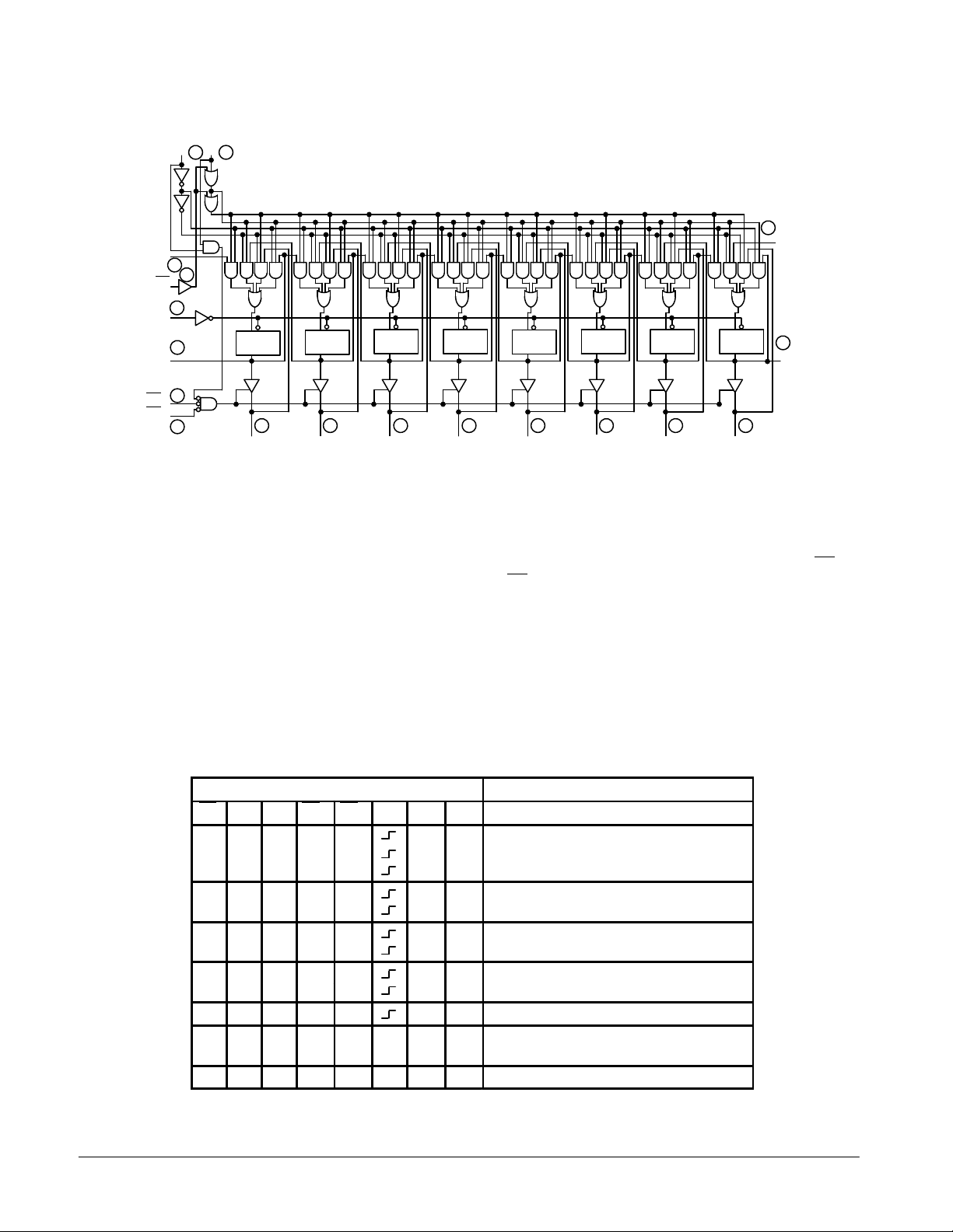
LOGIC DIAGRAM
DS
0
S1S
11
9
0
19
1
SR
12
OE
OE
CP
Q
D
I/O
CP
Q
0
8
0
2
1
2
3
D
CP
Q
13 15 16
I/O
1
I/O
D
CP
Q
67
2
FUNCTIONAL DESCRIPTION
The logic diagram and truth table indicate the functional
characteristics of the SN54/74LS323 Universal Shift/Storage
Register. This device is similar in operation to the
SN54/74LS299 except for synchronous reset. A partial list of
the common features are described below:
1. They use eight D-type edge-triggered flip-flops that respond only to the LOW-to-HIGH transition of the Clock
(CP). The only timing restriction, therefore, is that the mode
control (S0, S1) and data inputs (DS0, DS7, I/O0–I/O7) may
be stable at least a setup time prior to the positive transition
of the Clock Pulse.
18
I/O
D
CP
Q
14
3
I/O
D
CP
Q
4
I/O
D
CP
Q
5
I/O
D
CP
Q
45
6
I/O
D
CP
Q
7
2. When S0 = S1 = 1, I/O0–I/O7 are parallel inputs to flip-flops
Q0–Q7 respectively, and the outputs of Q0–Q7 are in the
high impedance state regardless of the state of OE
.
OE
2
An important unique feature of the SN54/74LS323 is a fully
Synchronous Reset that requires only to be stable at least one
setup time prior to the positive transition of the Clock Pulse.
17
DS
Q
7
7
or
1
TRUTH TABLE
INPUTS RESPONSE
SR S1S0OE1OE2CP DS0DS
L X X H X X X
L X X X H X X
7
=
=
=
=
L H H X X X X
L L X L L X X Synchronous Reset; Q0 = Q7 = LOW
L X L L L X X I/O voltage LOW
H L H X X D X Shift Right; D→Q0; Q0→Q1; etc.
H L H L L D X Shift Right; D→Q0 & I/O0; Q0→Q1 & I/O1; etc.
H H L X X X D Shift Left; D→Q7; Q7→Q6; etc.
H H L L L X D Shift Left; D→Q7 & I/O7; Q7→Q6 & I/O6; etc.
H H H X X X X Parallel Load I/On→Q
n
H L L H X X X X
H L L X H X X X
H L L L L X X X Hold; I/On = Q
H = HIGH Voltage Level
L = LOW Voltage Level
X = Immaterial
n
FAST AND LS TTL DATA
5-2
Page 3
SN54/74LS323
VILI
LOW Volt
V
pg
V
pg
V
MIN, I
MAX
V
pg
V
MIN, I
MAX
V
pg
V
V
V
V
pg
V
V
V
V
MAX, V
V
I
V
MAX, V
V
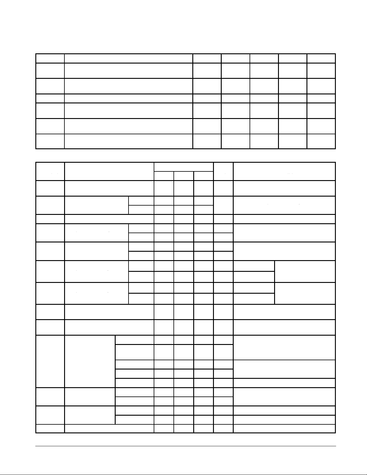
GUARANTEED OPERATING RANGES
Symbol Parameter Min Typ Max Unit
V
CC
T
A
I
OH
I
OL
I
OH
I
OL
DC CHARACTERISTICS OVER OPERATING TEMPERATURE RANGE (unless otherwise specified)
Symbol Parameter
V
IH
V
IK
OH
OH
OL
OL
I
OZH
I
OZL
I
IH
IL
I
OS
I
CC
Note 1: Not more than one output should be shorted at a time, nor for more than 1 second.
Supply Voltage 54
Operating Ambient Temperature Range 54
Output Current — High Q0, Q
Output Current — Low Q0, Q
Output Current — High I/O0–I/O
Output Current — Low I/O0–I/O
Input HIGH Voltage 2.0 V
nput
Input Clamp Diode Voltage –0.65 –1.5 V VCC = MIN, IIN = –18 mA
Output HIGH Voltage
I/O0–I/O
Output HIGH Voltage
Q0, Q
7
Output LOW Voltage
I/O0–I/O
Output LOW Voltage
Q0–Q
7
Output Off Current HIGH
I/O0–I/O
Output Off Current LOW
I/O0–I/O
Input HIGH Current
Input LOW Current
Short Circuit Current
(Note 1)
Power Supply Current 53 mA VCC = MAX
age
7
7
7
7
Others 20 µA
S0, S1,
I/O0–I/O
Others 0.1 mA
S0, S
I/O0–I/O
Others
S0, S
Qo, Q
I/O0–I/O
7
7
Q0, Q
7
I/O0–I/O
I/O0–I/O
1
1
7
7
7
7
7
Limits
Min Typ Max
54 0.7
74 0.8
54 2.4 3.2 V
74 2.4 3.1 V
54 2.5 3.4 V
74 2.7 3.4 V
54, 74 0.25 0.4 V IOL = 12 mA
74 0.35 0.5 V IOL = 24 mA
54, 74 0.4 V IOL = 4.0 mA
74 0.5 V IOL = 8.0 mA
7
7
–20 –100 mA VCC = MAX
7
–30 –130 mA VCC = MAX
74
74
54, 74 –0.4 mA
54
74
54
74
54
74
40 µA VCC = MAX, V
–400 µA VCC = MAX, V
40 µA
0.2 mA
0.1 mA VCC = MAX, VIN = 5.5 V
–0.4 mA
–0.8 mA
4.5
4.75
–55
0
Unit Test Conditions
Guaranteed Input HIGH Voltage for
All Inputs
Guaranteed Input LOW Voltage for
All Inputs
CC
CC
VCC = MAX, VIN = 2.7 V
CC
CC
=
=
=
=
5.0
5.0
25
25
=
OH
=
OH
VCC = VCC MIN,
IN
per Truth Table
VCC = VCC MIN,
IN
per Truth Table
= 2.7 V
OUT
= 0.4 V
OUT
= 7.0
IN
= 0.4
IN
5.25
–1.0
–2.6
=
=
5.5
125
70
4.0
8.0
12
24
or
IL
IH
or
IL
IH
V
°C
mA
mA
mA
FAST AND LS TTL DATA
5-3
Page 4
SN54/74LS323
L
p,
V
V
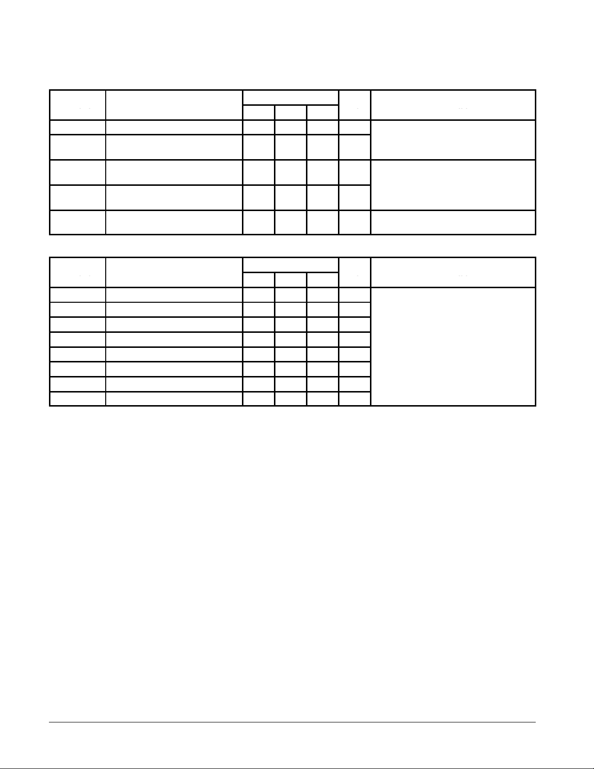
AC CHARACTERISTICS (T
Symbol Parameter
f
MAX
t
PHL
t
PLH
t
PHL
t
PLH
t
PZH
t
PZL
t
PHZ
t
PLZ
Maximum Clock Frequency 25 35 MHz
Propagation Delay, Clock
to Q0 or Q
Propagation Delay, Clock
to I/O0–I/O
Output Enable Time
Output Disable Time
= 25°C, VCC = 5.0 V)
A
7
7
AC SETUP REQUIREMENTS (T
Symbol Parameter
t
t
t
t
t
t
t
t
W
W
W
s
s
h
h
rec
Clock Pulse Width HIGH 25 ns
Clock Pulse Width LOW 15 ns
Clear Pulse Width LOW 20 ns
Data Setup Time 20 ns
Select Setup Time 35 ns
Data Hold Time 0 ns
Select Hold Time 10 ns
Recovery Time 20 ns
= 25°C, VCC = 5.0 V)
A
Limits
Min Typ Max
26
22
25
17
14
20
10
10
Limits
Min Typ Max
39
33
39
25
21
30
15
15
Unit Test Conditions
ns
ns
ns
ns CL = 5.0 pF
Unit Test Conditions
CL = 15 pF
CL = 45 pF,
RL = 667 Ω
= 5.0
CC
FAST AND LS TTL DATA
5-4
Page 5
SN54/74LS323
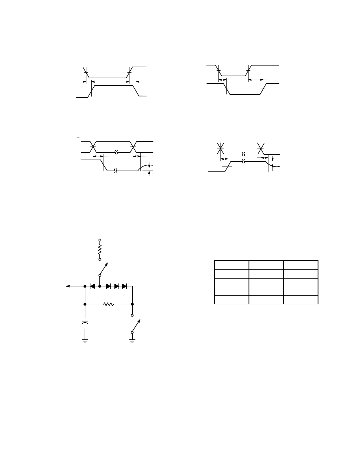
3-STATE WAVEFORMS
V
1.3 V 1.3 V
IN
t
PLH
V
OUT
1.3 V
Figure 1 Figure 2
V
E
V
E
1.5 V 1.5 V
V
OUT
Figure 3 Figure 4
V
CC
t
PZL
1.5 V
1.3 V
0.5 V
t
PHL
t
PLZ
≈
1.5 V
V
OL
AC LOAD CIRCUIT
t
PHZ
1.3 V
t
PHL
1.3 V
≥
0.5 V
V
≈
OH
1.5 V
1.3 V
V
IN
t
PLH
V
OUT
V
E
V
E
t
PZH
V
OUT
1.3 V
1.5 V 1.5 V
1.5 V
TO OUTPUT
UNDER TEST
R
L
SW1
Ω
5 k
SW2CL*
* Includes Jig and Probe Capacitance.
Figure 5
SWITCH POSITIONS
SYMBOL SW1 SW2
t
PZH
t
PZL
t
PLZ
t
PHZ
Open Closed
Closed Open
Closed Closed
Closed Closed
FAST AND LS TTL DATA
5-5
 Loading...