

Page 1
8-BIT SHIFT REGISTERS
WITH SIGN EXTEND
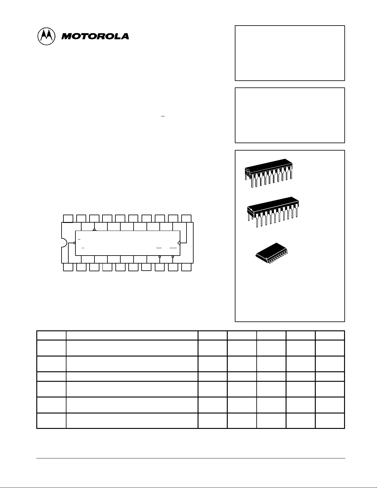
These 8-bit shift registers have multiplexed input/output data ports to
accomplish full 8-bit data handling in a single 20-pin package. Serial data may
enter the shift-right register through either D0 or D1 inputs as selected by the
data select pin. A serial output is also provided. Synchronous parallel loading
is achieved by taking the register enable and the S/P
the three-state input/output ports in the data input mode. Data is entered on
the low-to-high clock transition. The data extend function repeats the sign in
the QA flip-flop during shifting. An overriding clear input clears the internal
registers when taken low whether the outputs are enabled or off. The output
enable does not affect synchronous operation of the register.
• Multiplexed Inputs/Outputs Provide Improved Bit Density
• Sign Extend Function
• Direct Overriding Clear
• 3-State Outputs Drive Bus Lines Directly
(TOP VIEW)
DATA
V
CC
20
123456
REGISTER
ENABLE
SIGN
SELECT
19
DS SE D1 B/QBD/QDF/QFH/GHQ/
G
S/P D0 A/QAC/QCE/QEG/QGOE CLR
S/P
D1 B/QBD/QDF/QFH/QHQ/HCLOCK
EXTEND
18 17 16 15 14 13
7
D0 A/QAC/QCE/QEG/Q
inputs low. This places
12 11
H
CK
8 910
OUTPUT
ENABLE
CLEAR GND
G
SN54/74LS322A
8-BIT SHIFT REGISTERS
WITH SIGN EXTEND
LOW POWER SCHOTTKY
J SUFFIX
CERAMIC
20
1
20
1
20
1
CASE 732-03
N SUFFIX
PLASTIC
CASE 738-03
DW SUFFIX
CASE 751D-03
SOIC
ORDERING INFORMATION
SN54LSXXXJ Ceramic
SN74LSXXXN Plastic
SN74LSXXXDW SOIC
GUARANTEED OPERATING RANGES
Symbol Parameter Min Typ Max Unit
V
T
I
I
I
I
CC
A
OH
OL
OH
OL
Supply Voltage 54
Operating Ambient Temperature Range 54
Output Current — High QH′ 54, 74 –0.4 mA
Output Current — Low QH′
Output Current — High QA–Q
Output Current — Low QA–Q
QH′
QA–Q
QA–Q
H
H
H
H
74
74
54
74
54
74
54
74
4.5
4.75
–55
0
5.0
5.0
25
25
5.5
5.25
125
70
4.0
8.0
–1.0
–2.6
12
24
FAST AND LS TTL DAT A
5-1
V
°C
mA
mA
mA
Page 2
SN54/74LS322A
OUTPUT
Shift Right
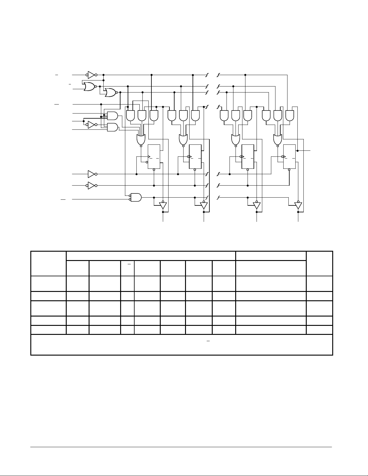
BLOCK DIAGRAM
REGISTER
ENABLE
G
SIGN
EXTEND
SE
DATA
SELECT
DS
CLOCK
CLEAR
OUTPUT
ENABLE
OE
S/P
D1
D0
(1)
(2)
(18)
(17)
(19)
(3)
(11)
(9)
(8)
D
CK
CLR
FOUR
IDENTICAL
CHANNELS
B/Q
B
NOT
SHOWN
CK
D
CLR
Q
CK
Q
(7)(16)
G/Q
G
D
CLR
Q
Q
(4)
A/Q
A
CK
D
CLR
Q
Q
Q
Q
(13)
H/Q
(12)
Q
H
H
FUNCTION TABLE
INPUTS INPUTS/OUTPUTS
OPERATION
CLEAR
Clear L H X X X L X L L L L L
L X H X X L X L LLL L
Hold H H X X X L X Q
Sign Extend H L H L X L ↑ Q
Load H L L X X X ↑ a b c h h
When the output enable is high, the eight input/output terminals are disabled to the high-impedance state; however, sequential operation or
clearing of the register is not affected. If both the register enable input and the S/P
cleared while the eight input/output terminals are disabled to the high-impedance state.
H = HIGH Level (steady state)
L = LOW Level (steady state)
X = Irrelevant (any input, including transitions)
↑ = Transition from LOW to HIGH level
Q
Q
D0, D1 = the level of steady-state inputs at inputs D0 and D1 respectively
a…h = the level of steady-state inputs at inputs A through H respectively
= the level of QA through QH, respectively, before the indicated steady-state conditions were established
A0…QH0
= the level of QA through QH, respectively, before the most recent ↑transition of the clock
An…QHn
REGISTER
ENABLE
S/P
SIGN
EXTEND
DATA
SELECT
OUTPUT
ENABLE
CLOCK A/QAB/QBC/QC H/Q
H L H H L L ↑ D
H L H H H L ↑ D
input are low while the clear input is low, the register is
…
A0QB0QC0
Q
0
AnQBnQGn
Q
1
AnQBnQGn
Q
H0
AnQAnQBnQGn
H
QH′
Q
Q
Q
Q
H0
Gn
Gn
Gn
FAST AND LS TTL DATA
5-2
Page 3
SN54/74LS322A
VILI
LOW Volt
V
pg
V
pg
V
MIN, I
MAX
V
pg
V
MIN, I
MAX
V
pg
V
V
V
V
pg
V
V
V
I
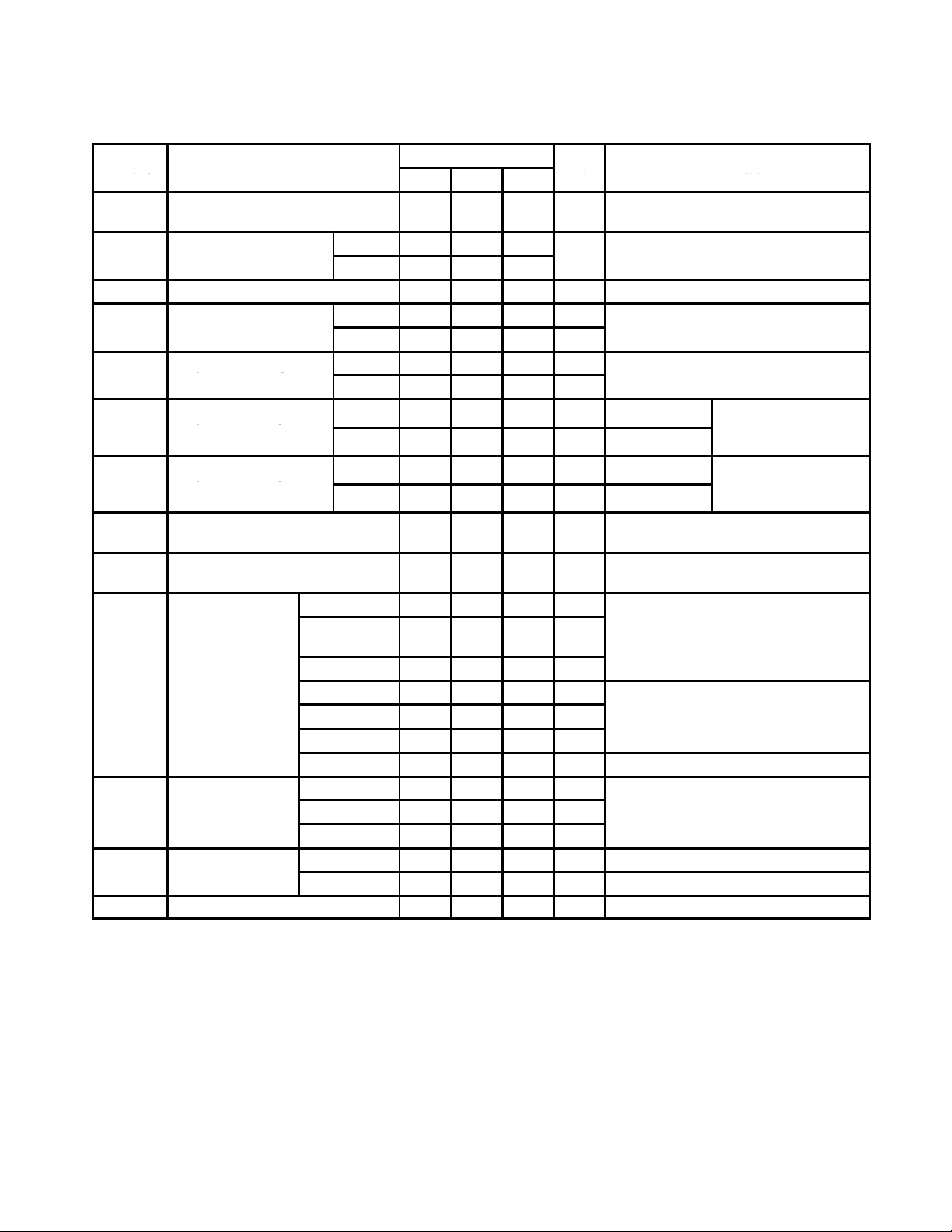
DC CHARACTERISTICS OVER OPERATING TEMPERATURE RANGE (unless otherwise specified)
Limits
Symbol Parameter
V
IH
V
IK
OH
OH
OL
OL
I
OZH
I
OZL
I
IH
I
IL
OS
I
CC
Note 1: Not more than one output should be shorted at a time, nor for more than 1 second.
Input HIGH Voltage 2.0 V
nput
Input Clamp Diode Voltage –0.65 –1.5 V VCC = MIN, IIN = –18 mA
Output HIGH Voltage
QA–Q
H
Output HIGH Voltage
QH′
Output LOW Voltage
QA–Q
H
Output LOW Voltage
QH′
Output Off Current HIGH
QA–Q
H
Output Off Current LOW
QA–Q
H
Input HIGH Current
Input LOW Current
Short Circuit Current
(Note 1)
Power Supply Current 60 mA VCC = MAX
age
Other 20 µA
A–H,
Data Select
Sign Extend 60 µA
Other 0.1 mA
Data Select 0.2 mA
Sign Extend 0.3 mA
A–H 0.1 mA VCC = MAX, VIN = 5.5 V
Other –0.4 mA
Data Select –0.8 mA
Sign Extend –1.2 mA
QH′ –20 –100 mA VCC = MAX
QA–Q
54 0.7
74 0.8
54 2.4 3.2 V
74 2.4 3.2 V
54 2.5 3.4 V
74 2.7 3.4 V
54, 74 0.25 0.4 V IOL = 12 mA
74 0.35 0.5 V IOL = 24 mA
54, 74 0.4 V IOL = 4.0 mA
74 0.5 V IOL = 8.0 mA
H
Min Typ Max
–400 µA VCC = MAX, V
–30 –130 mA VCC = MAX
Unit Test Conditions
Guaranteed Input HIGH Voltage for
All Inputs
Guaranteed Input LOW Voltage for
All Inputs
=
CC
=
CC
40 µA VCC = MAX, V
40 µA
VCC = MAX, VIN = 2.7 V
VCC = MAX, VIN = 7.0 V
VCC = MAX, VIN = 0.4 V
OH
OH
=
=
VCC = VCC MIN,
=
IN
per Truth Table
VCC = VCC MIN,
=
IN
per Truth Table
= 2.7 V
OUT
= 0.4 V
OUT
or
IL
IH
or
IL
IH
FAST AND LS TTL DATA
5-3
Page 4
SN54/74LS322A
V
V
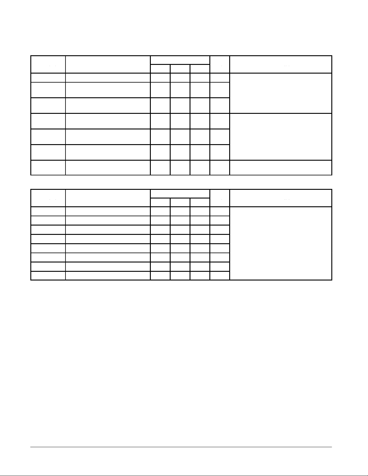
AC CHARACTERISTICS (T
Symbol Parameter
f
MAX
t
PHL
t
PLH
t
PHL
t
PHL
t
PLH
t
PHL
t
PZH
t
PZL
t
PHZ
t
PLZ
Maximum Clock Frequency 25 35 MHz
Propagation Delay, Clock
to QH′
Propagation Delay, Clear
to QH′
Propagation Delay, Clock
to QA–Q
Propagation Delay, Clear
to QA–Q
Output Enable Time
Output Disable Time
= 25°C, VCC = 5.0 V)
A
H
H
AC SETUP REQUIREMENTS (T
Symbol Parameter
t
t
t
t
t
t
t
t
W
W
W
s
s
h
h
rec
Clock Pulse Width HIGH 25 ns
Clock Pulse Width LOW 15 ns
Clear Pulse Width LOW 20 ns
Data Setup Time 20 ns
Select Setup Time 15 ns
Data Hold Time 0 ns
Select Hold Time 10 ns
Recovery Time 20 ns
= 25°C, VCC = 5.0 V)
A
Limits
Min Typ Max
26
22
27 35 ns
22
16
22 35 ns
15
15
15
15
Limits
Min Typ Max
35
33
33
25
35
35
25
25
Unit Test Conditions
ns
ns
ns
ns CL = 5.0 pF
Unit Test Conditions
CL = 15 pF
CL = 45 pF,
RL = 667 Ω
= 5.0
CC
DEFINITIONS OF TERMS
SETUP TIME (ts) — is defined as the minimum time required
for the correct logic level to be present at the logic input prior to
the clock transition from LOW-to-HIGH in order to be recognized and transferred to the outputs.
HOLD TIME (th) — is defined as the minimum time following
the clock transition from LOW-to-HIGH that the logic level
must be maintained at the input in order to ensure continued
FAST AND LS TTL DATA
recognition. A negative HOLD TIME indicates that the correct
logic level may be released prior to the clock transition from
LOW-to-HIGH and still be recognized.
RECOVERY TIME (t
) — is defined as the minimum time
rec
required between the end of the reset pulse and the clock
transition from LOW-to-HIGH in order to recognize and
transfer HIGH Data to the Q outputs.
5-4
 Loading...