

Page 1
DECADE COUNTER;
4-BIT BINARY COUNTER
The SN54/74LS290 and SN54/74LS293 are high-speed 4-bit ripple type
counters partitioned into two sections. Each counter has a divide-by-two section and either a divide-by-five (LS290) or divide-by-eight (LS293) section
which are triggered by a HIGH-to-LOW transition on the clock inputs. Each
section can be used separately or tied together (Q to CP
Bi-quinary , or Modulo-16 counters. Both of the counters have a 2-input gated
Master Reset (Clear), and the LS290 also has a 2-input gated Master Set
(Preset 9).
• Corner Power Pin Versions of the LS90 and LS93
• Low Power Consumption . . . Typically 45 mW
• High Count Rates . . . Typically 42 MHz
• Choice of Counting Modes . . . BCD, Bi-Quinary , Binary
• Input Clamp Diodes Limit High Speed Termination Effects
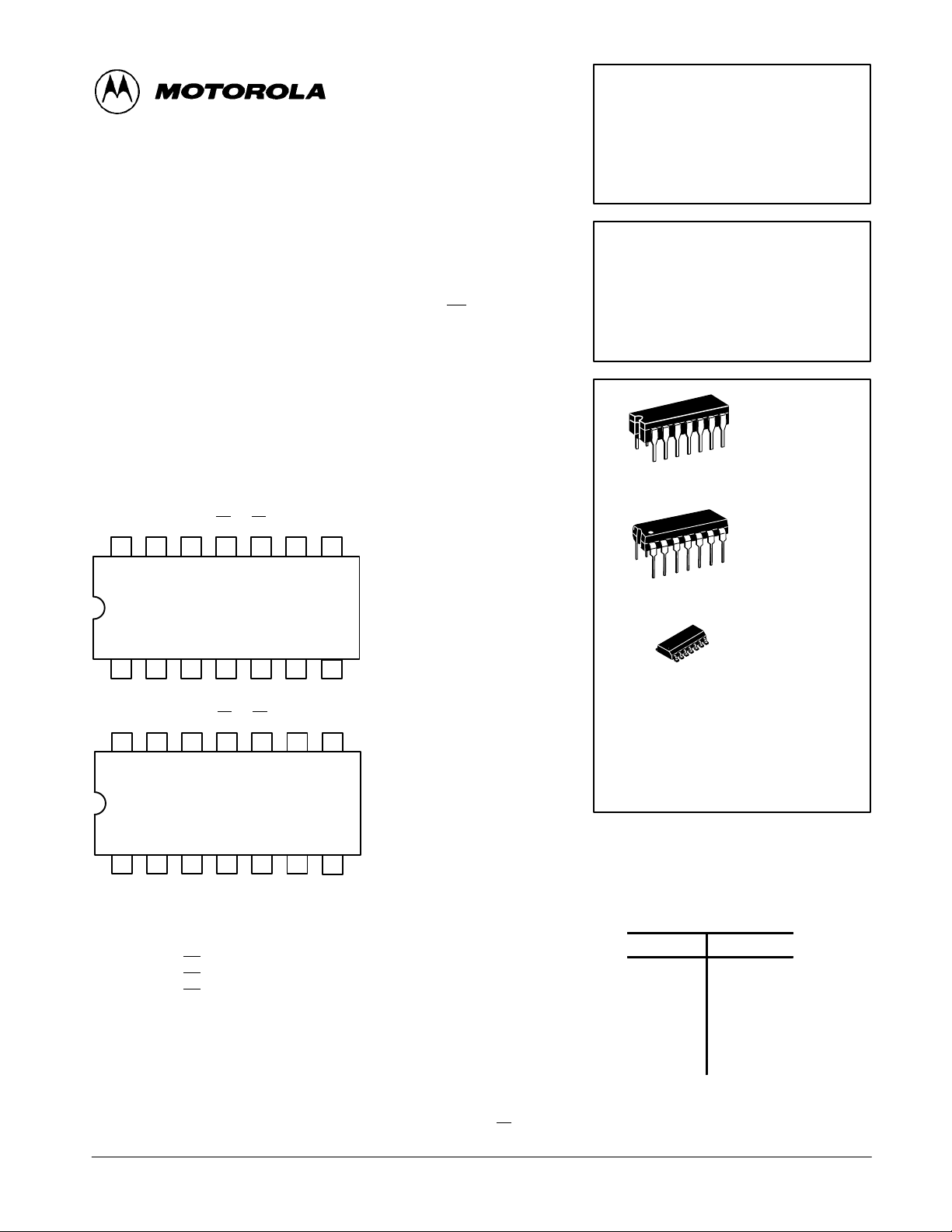
CONNECTION DIAGRAM DIP (TOP VIEW)
VCCMR MR CP
14 13 12 11 10 9
123456
MS NC MS Q2Q1NC GND
1CP0Q0Q3
LS290
8
NOTE:
The Flatpak version
has the same pinouts
(Connection Diagram) as
the Dual In-Line Package.
7
)to form BCD,
SN54/74LS290
SN54/74LS293
DECADE COUNTER;
4-BIT BINARY COUNTER
LOW POWER SCHOTTKY
J SUFFIX
CERAMIC
14
1
14
1
14
1
CASE 632-08
N SUFFIX
PLASTIC
CASE 646-06
D SUFFIX
SOIC
CASE 751A-02
VCCMR MR CP
14 13 12 11 10 9
1CP0Q0Q3
LS293
123456
NC NC NC Q2Q1NC GND
PIN NAMES LOADING (Note a)
CP
0
CP1 Clock (Active LOW going edge) Input to ÷5 Section (LS290). 0.05 U.L. 2.0 U.L.
CP1 Clock (Active LOW going edge) Input to ÷8 Section (LS293). 0.05 U.L. 1.0 U.L.
MR1, MR2 Master Reset (Clear) Inputs 0.5 U.L. 0.25 U.L.
MS1, MS2 Master Set (Preset-9, LS290) Inputs 0.5 U.L. 0.25 U.L.
Q0 Output from ÷2 Section (Notes b & c) 10 U.L. 5 (2.5) U.L.
Q1, Q2, Q3 Outputs from ÷5 & ÷8 Sections (Note b) 10 U.L. 5 (2.5) U.L.
NOTES:
a) 1 TTL Unit Load (U.L.) = 40 µA HIGH/1.6 mA LOW.
b) The Output LOW drive factor is 2.5 U.L. for Military (54) and 5 U.L. for Commercial (74) Temperature Ranges.
c) The Q0 Outputs are guaranteed to drive the full fan-out plus the CP
Clock (Active LOW going edge) Input to ÷2 Section. 0.05 U.L. 1.5 U.L.
8
7
Input of the device.
1
ORDERING INFORMATION
SN54LSXXXJ Ceramic
SN74LSXXXN Plastic
SN74LSXXXD SOIC
HIGH
LOW
FAST AND LS TTL DAT A
5-1
Page 2
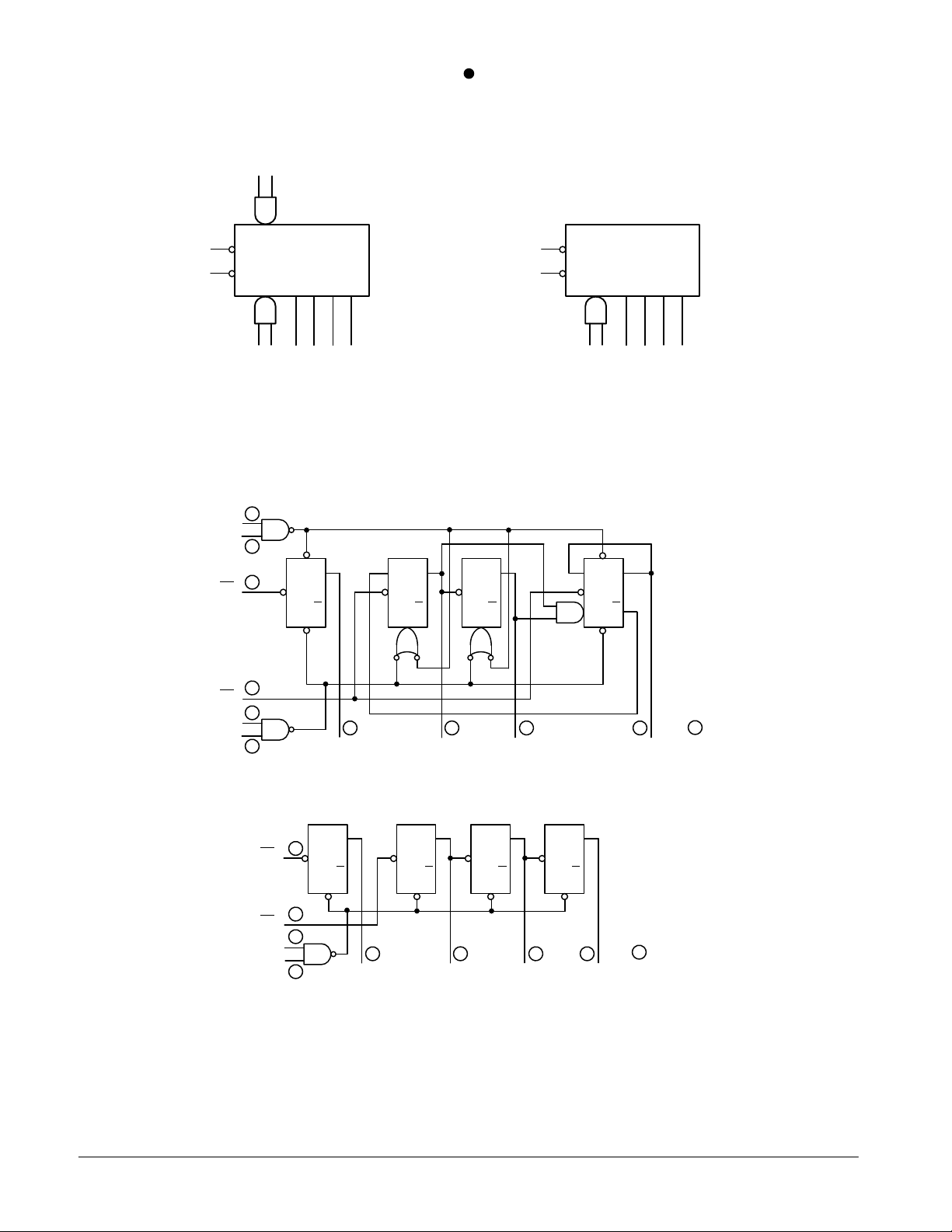
LOGIC SYMBOL
SN54/74LS290 D SN54/74LS293
LS290 LS293
13
12
LOGIC DIAGRAMS
10
11
MS
CP
0
CP
1
MR Q0Q1Q2Q
12
12 13 9 5 4 8
VCC = PIN 14
GND = PIN 7
NC = PINS 2, 6
1
MS
1
MS
2
3
10
CP
0
11
CP
1
12
MR
1
MR
2
13
3
S
D
J
QJ
CP
Q
C
D
Q
0
QJ
CP
Q
K
C
D
Q
CP
10
11
0
CP
1
MR Q0Q1Q2Q
3
12
12 13 9 5 4 8
VCC = PIN 14
GND = PIN 7
NC = PINS 1, 2, 3, 6
LS290
S
CP
D
Q
Q
C
D
VCC = PIN 14
GND = PIN 7
8459
Q
3
= PIN NUMBERS
QR
CP
Q
KS
C
D
1
Q
2
CP
CP
MR
MR
J
Q
10
CP
0
1
Q
K
C
D
11
12
1
2
13
Q
0
LS293
J
CP
K
Q
Q
C
D
J
Q
CP
Q
K
C
D
Q
1
Q
2
FAST AND LS TTL DATA
5-2
J
CP
K
Q
Q
C
D
VCC = PIN 14
GND = PIN 7
8459
Q
3
= PIN NUMBERS
Page 3
SN54/74LS290 D SN54/74LS293
COUNT
COUNT
FUNCTIONAL DESCRIPTION
The LS290 and LS293 are 4-bit ripple type Decade, and
4-Bit Binary counters respectively. Each device consists of
four master/slave flip-flops which are internally connected to
provide a divide-by-two section and a divide-by-five (LS290)
or divide-by-eight (LS293) section. Each section has a
separate clock input which initiates state changes of the
counter on the HIGH-to-LOW clock transition. State changes
of the Q outputs do not occur simultaneously because of
internal ripple delays. Therefore, decoded output signals are
subject to decoding spikes and should not be used for clocks
or strobes. The Q0 output of each device is designed and
specified to drive the rated fan-out plus the CP
device.
A gated AND asynchronous Master Reset (MR1 ⋅ MR2) is
provided on both counters which overrides the clocks and
resets (clears) all the flip-flops. A gated AND asynchronous
Master Set (MS1 ⋅ MS2) is provided on the LS290 which
overrides the clocks and the MR inputs and sets the outputs to
nine (HLLH).
Since the output from the divide-by-two section is not
internally connected to the succeeding stages, the devices
may be operated in various counting modes:
LS290
A. BCD Decade (8421) Counter — the CP
input of the
1
input must be
1
externally connected to the Q0 output. The CP
input
0
receives the incoming count and a BCD count sequence is
produced.
B. Symmetrical Bi-quinary Divide-By-Ten Counter — The Q
output must be externally connected to the CP
input count is then applied to the CP
input. The
0
input and a
1
divide-by-ten square wave is obtained at output Q0.
C. Divide-By-Two and Divide-By-Five Counter — No external
interconnections are required. The first flip-flop is used as a
binary element for the divide-by-two function (CP
input and Q0 as the output). The CP
input is used to obtain
1
as the
0
binary divide-by-five operation at the Q3 output.
LS293
A. 4-Bit Ripple Counter — The output Q0 must be externally
connected to input CP
to input CP
. Simultaneous division of 2, 4, 8, and 16 are
0
. The input count pulses are applied
1
performed at the Q0, Q1, Q2, and Q3 outputs as shown in
the truth table.
B. 3-Bit Ripple Counter — The input count pulses are applied
to input CP
. Simultaneous frequency divisions of 2, 4, and
1
8 are available at the Q1, Q2, and Q3 outputs. Independent
use of the first flip-flop is available if the reset function
coincides with reset of the 3-bit ripple-through counter.
3
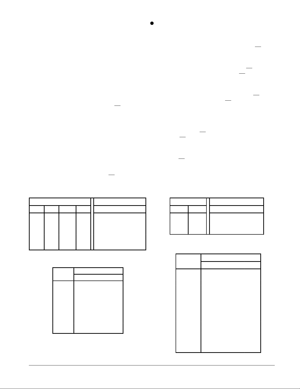
LS290 MODE SELECTION
RESET/SET INPUTS OUTPUTS
MR1MR
H H L X L L L L
H H X L L LL L
X X H H HLLH
L X L X Count
X L X L Count
L X X L Count
X L L X Count
2
MS1MS
2
Q0Q1Q
Q
2
3
LS290
BCD COUNT SEQUENCE
OUTPUT
Q0Q1Q
0 L L L L
1 H LLL
2 LHLL
3 HHLL
4 LLHL
5 HLHL
6 LHH L
7 HHH L
8 LLLH
9 HLLH
NOTE: Output Q0 is connected to Input CP
for BCD count.
H = HIGH Voltage Level
L = LOW Voltage Level
X = Don’t Care
Q
2
3
1
LS293 MODE SELECTION
RESET INPUTS OUTPUTS
MR
H H L L L L
L H Count
H L Count
L L Count
MR
1
Q
Q
2
0
Q
1
2
TRUTH TABLE
OUTPUT
Q0Q
0 L L L L
1 H LL L
2 LHL L
3 HHL L
4 LLH L
5 HLH L
6 LHH L
7 HHH L
8 LLL H
9 HLL H
10 L HL H
11 H HL H
12 L LH H
13 H LH H
14 L HH H
15 H H H H
Note: Output Q0 connected to input CP1.
Q
1
2
Q
3
Q
3
FAST AND LS TTL DATA
5-3
Page 4
SN54/74LS290 • SN54/74LS293
VILI
LOW Volt
V
pg
VOHOutput HIGH Volt
CC
,
OH
,
IN IH
VOLOutput LOW Volt
V
V
V
IIHI
HIGH C
t
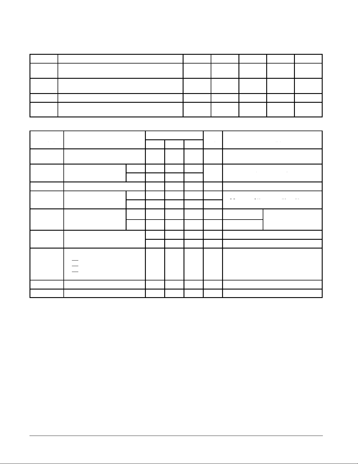
GUARANTEED OPERATING RANGES
Symbol Parameter Min Typ Max Unit
V
CC
T
A
I
OH
I
OL
DC CHARACTERISTICS OVER OPERATING TEMPERATURE RANGE (unless otherwise specified)
Symbol Parameter
V
IH
V
IK
I
IL
I
OS
I
CC
Note 1: Not more than one output should be shorted at a time, nor for more than 1 second.
Supply Voltage 54
Operating Ambient Temperature Range 54
Output Current — High 54, 74 –0.4 mA
Output Current — Low 54
Limits
Min Typ Max
Input HIGH Voltage 2.0 V
nput
Input Clamp Diode Voltage –0.65 –1.5 V VCC = MIN, IIN = –18 mA
nput
Input LOW Current
MS, MR
CP
0
CP
(LS290)
1
CP1 (LS293)
Short Circuit Current (Note 1) –20 –100 mA VCC = MAX
Power Supply Current 15 mA VCC = MAX
age
age
age
urren
54
74
54 2.5 3.5 V
74 2.7 3.5 V
54, 74 0.25 0.4 V IOL = 4.0 mA
74 0.35 0.5 V IOL = 8.0 mA
74
74
74
0.7
0.8
20 µA VCC = MAX, VIN = 2.7 V
0.1 mA VCC = MAX, VIN = 7.0 V
–0.4
–2.4
–3.2
–1.6
4.5
4.75
–55
0
Unit Test Conditions
Guaranteed Input HIGH Voltage for
All Inputs
Guaranteed Input LOW Voltage for
All Inputs
VCC = MIN, IOH = MAX, VIN = V
or VIL per Truth Table
mA VCC = MAX, VIN = 0.4 V
5.0
5.0
25
25
5.5
5.25
125
70
4.0
8.0
VCC = VCC MIN,
=
IN
IL
per Truth Table
or
IH
IH
V
°C
mA
FAST AND LS TTL DATA
5-4
Page 5
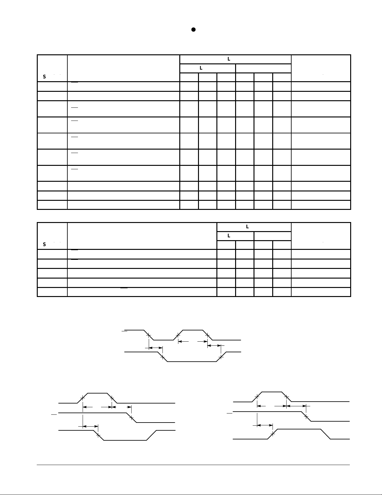
SN54/74LS290 D SN54/74LS293
AC CHARACTERISTICS (T
Symbol Parameter
f
MAX
f
MAX
t
PLH
t
PHL
t
PLH
t
PHL
t
PLH
t
PHL
t
PLH
t
PHL
t
PLH
t
PHL
t
PHL
t
PHL
t
PHL
CP0 Input Clock Frequency 32 32 MHz
CP1 Input Clock Frequency 16 16 MHz
Propagation Delay,
CP
Input to Q0 Output
0
CP0 Input to Q3 Output
CP1 Input to Q1 Output
CP
Input to Q2 Output
1
CP1 Input to Q3 Output
MS Input to Q0 and Q3 Outputs 20 30 ns
MS Input to Q1 and Q2 Outputs 26 40 ns
MR Input to Any Output 26 40 26 40 ns
AC SETUP REQUIREMENTS (T
Symbol Parameter
t
W
t
W
t
W
t
W
t
rec
RECOVERY TIME (t
recognize and transfer HIGH data to the Q outputs.
CP0
Pulse Width
CP1
Pulse Width
MS Pulse Width 15 ns
MR Pulse Width 15 15 ns
Recovery Time MR to CP 25 25 ns
) is defined as the minimum time required between the end of the reset pulse and the clock transition form HIGH-to-LOW in order to
rec
= 25°C, VCC = 5.0 V, CL = 15 pF)
A
= 25°C, VCC = 5.0 V)
A
Limits
LS290 LS293
Min Typ Max Min Typ Max
10
16
12
18
32
48
34
50
10
16
14
21
21
32
23
35
21
32
23
35
LS290 LS293
Min Max Min Max
15 15 ns
30 30 ns
Limits
10
12
46
46
10
14
21
23
34
34
16
18
70
70
16
21
32
35
51
51
Unit
ns
ns
ns
ns
ns
Unit
MR & MS
CP
Q
*CP
1.3 V 1.3 V
t
PHL
Q
*The number of Clock Pulses required between the t
1.3 V 1.3 V
t
PHL
t
W
1.3 V
t
rec
1.3 V
Figure 2 Figure 3
FAST AND LS TTL DATA
AC WAVEFORMS
t
W
Figure 1
PHL
and t
measurements can be determined from the appropriate Truth Tables.
PLH
5-5
t
PLH
1.3 V1.3 V
MS
CP
Q0 ⋅Q
3
(LS290)
t
PLH
1.3 V1.3 V
t
W
1.3 V
t
rec
1.3 V
 Loading...