

Datasheet SN74LS273DWR2, SN74LS273FN, SN74LS273H, SN74LS273M, SN74LS273MEL Datasheet (MOTOROLA)
...Page 1
Semiconductor Components Industries, LLC, 1999
December, 1999 – Rev. 6
1 Publication Order Number:
SN74LS273/D
SN74LS273
Octal D Flip-Flop
with Clear
The SN74LS273 is a high-speed 8-Bit Register. The register
consists of eight D-Type Flip-Flops with a Common Clock and an
asynchronous active LOW Master Reset. This device is supplied in a
20-pin package featuring 0.3 inch lead spacing.
• 8-Bit High Speed Register
• Parallel Register
• Common Clock and Master Reset
• Input Clamp Diodes Limit High-Speed Termination Effects
GUARANTEED OPERATING RANGES
Symbol Parameter Min Typ Max Unit
V
CC
Supply Voltage 4.75 5.0 5.25 V
T
A
Operating Ambient
T emperature Range
0 25 70 °C
I
OH
Output Current – High –0.4 mA
I
OL
Output Current – Low 8.0 mA
LOW
POWER
SCHOTTKY
Device Package Shipping
ORDERING INFORMATION
SN74LS273N 16 Pin DIP 1440 Units/Box
SN74LS273DW 16 Pin
SOIC
DW SUFFIX
CASE 751D
http://onsemi.com
2500/Tape & Reel
PLASTIC
N SUFFIX
CASE 738
20
1
20
1
Page 2
SN74LS273
http://onsemi.com
2
18 17 16 15 14 13
123456
7
20 19
8
V
CC
MR
Q7D7D6Q
6
D
5
Q
5
D
4
Q0D0D1Q1Q2D2D
3
910
Q
3
GND
12 11
Q
4
CP
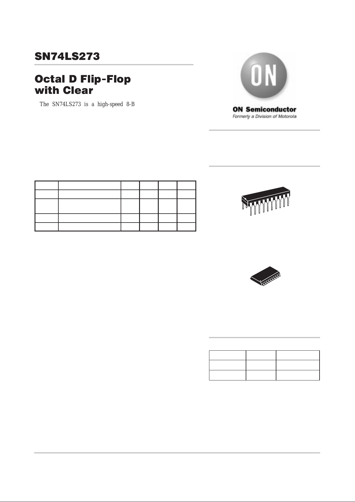
CONNECTION DIAGRAM DIP (TOP VIEW)
Clock (Active HIGH Going Edge) Input
Data Inputs
Master Reset (Active LOW) Input
Register Outputs
CP
D
0
– D
7
MR
Q0 – Q
7
0.5 U.L.
0.5 U.L.
0.5 U.L.
10 U.L.
0.25 U.L.
0.25 U.L.
0.25 U.L.
5 U.L.
NOTES:
a) 1 TTL Unit Load (U.L.) = 40 mA HIGH/1.6 mA LOW.
HIGH LOW
(Note a)LOADING
PIN NAMES
TRUTH TABLE
MR CP DxQ
x
L X X L
H H H
H L L
H = HIGH Logic Level
L = LOW Logic Level
X = Immaterial
LOGIC DIAGRAM
CP
MR
D
0
D
1
D
2
D
3
D
4
D
5
D
6
D
7
Q
0
Q
1
Q
2
Q
3
Q
4
Q
5
Q
6
Q
7
CP D
CD
Q
CP D
CD
Q
CP D
CD
Q
CP D
CD
Q
CP D
CD
Q
CP D
CD
Q
CP D
CD
Q
CP D
CD
Q
14
1
26
73 84
5 9
11
12
13
15
VCC = PIN 20
GND = PIN 10
= PIN NUMBERS
17 18
16 19
Page 3
SN74LS273
http://onsemi.com
3
FUNCTIONAL DESCRIPTION
The SN74LS273 is an 8-Bit Parallel Register with a
common Clock and common Master Reset.
When the MR input is LOW, the Q outputs are LOW,
independent of the other inputs. Information meeting the
setup and hold time requirements of the D inputs is
transferred to the Q outputs on the LOW-to-HIGH transition
of the clock input.
DC CHARACTERISTICS OVER OPERATING TEMPERATURE RANGE (unless otherwise specified)
Limits
Symbol Parameter
Min Typ Max
Unit Test Conditions
V
IH
Input HIGH Voltage 2.0 V
Guaranteed Input HIGH Voltage for
All Inputs
V
IL
Input LOW Voltage
0.8
V
Guaranteed Input LOW Voltage for
All Inputs
V
IK
Input Clamp Diode Voltage –0.65 –1.5 V VCC = MIN, IIN = –18 mA
V
OH
Output HIGH Voltage 2.7 3.5 V
VCC = MIN, IOH = MAX, VIN = V
IH
or VIL per Truth Table
p
0.25 0.4 V IOL = 4.0 mA
VCC = VCC MIN,
VOLOutput LOW Voltage
0.35 0.5 V IOL = 8.0 mA
V
IN
=
V
IL
or
V
IH
per Truth Table
p
20 µA VCC = MAX, VIN = 2.7 V
IIHInput HIGH Current
0.1 mA VCC = MAX, VIN = 7.0 V
I
IL
Input LOW Current –0.4 mA VCC = MAX, VIN = 0.4 V
I
OS
Short Circuit Current (Note 1) –20 –100 mA VCC = MAX
I
CC
Power Supply Current 27 mA VCC = MAX
Note 1: Not more than one output should be shorted at a time, nor for more than 1 second.
AC CHARACTERISTICS (T
A
= 25°C, VCC = 5.0 V)
Limits
Symbol Parameter
Min Typ Max
Unit Test Conditions
f
MAX
Maximum Input Clock Frequency 30 40 MHz Figure 1
t
PHL
Propagation Delay, MR to Q Output 18 27 ns Figure 2
t
PLH
t
PHL
Propagation Delay, Clock to Output
17
18
27
27
ns Figure 1
AC SETUP REQUIREMENTS (T
A
= 25°C, VCC = 5.0 V)
Limits
Symbol Parameter
Min Typ Max
Unit Test Conditions
t
w
Pulse Width, Clock or Clear 20 ns Figure 1
t
s
Data Setup Time 20 ns Figure 1
t
h
Hold Time 5.0 ns Figure 1
t
rec
Recovery Time 25 ns Figure 2
Page 4

SN74LS273
http://onsemi.com
4
1.3 V
*The shaded areas indicate when the input is permitted to
*change for predictable output performance.
1.3 V
1.3 V
1.3 V
1.3 V
1.3 VCP
D
Q
n
ts(H)
t
h
(H)
t
s
(L)
t
h
(L)
1/f max
t
PLH
t
PLH
t
PHL
t
PHL
MR
CP
Q
n
Q
n
1.3 V
1.3 V
1.3 V
1.3 V1.3 V
1.3 V
t
rec
t
PHL
t
PLH
t
W
1.3 V
1.3 V
1.3 V
*
t
W
Figure 1. Clock to Output Delays, Clock Pulse Width,
Frequency, Setup and Hold Times Data to Clock
Figure 2. Master Reset to Output Delay, Master Reset
Pulse Width, and Master Reset Recovery Time
AC WAVEFORMS
DEFINITION OF TERMS
SETUP TIME (ts) — is defined as the minimum time
required for the correct logic level to be present at the logic
input prior to the clock transition from LOW-to-HIGH in
order to be recognized and transferred to the outputs.
HOLD TIME (t
h
) — is defined as the minimum time
following the clock transition from LOW-to-HIGH that the
logic level must be maintained at the input in order to ensure
continued recognition. A negative HOLD TIME indicates
that the correct logic level may be released prior to the clock
transition from LOW-to-HIGH and still be recognized.
RECOVER Y TIME (t
rec
) — is defined as the minimum time
required between the end of the reset pulse and the clock
transition from LOW-to-HIGH in order to recognize and
transfer HIGH data to the Q outputs.
Page 5

SN74LS273
http://onsemi.com
5
P ACKAGE DIMENSIONS
N SUFFIX
PLASTIC PACKAGE
CASE 738–03
ISSUE E
NOTES:
1. DIMENSIONING AND TOLERANCING PER ANSI
Y14.5M, 1982.
2. CONTROLLING DIMENSION: INCH.
3. DIMENSION L TO CENTER OF LEAD WHEN
FORMED PARALLEL.
4. DIMENSION B DOES NOT INCLUDE MOLD
FLASH.
M
L
J
20 PL
M
B
M
0.25 (0.010) T
DIM MIN MAX MIN MAX
MILLIMETERSINCHES
A 25.66 27.171.010 1.070
B 6.10 6.600.240 0.260
C 3.81 4.570.150 0.180
D 0.39 0.550.015 0.022
G 2.54 BSC0.100 BSC
J 0.21 0.380.008 0.015
K 2.80 3.550.110 0.140
L 7.62 BSC0.300 BSC
M 0 15 0 15
N 0.51 1.010.020 0.040
____
E
1.27 1.770.050 0.070
1
11
10
20
–A–
SEATING
PLANE
K
N
FG
D
20 PL
–T–
M
A
M
0.25 (0.010) T
E
B
C
F
1.27 BSC0.050 BSC
Page 6

SN74LS273
http://onsemi.com
6
D SUFFIX
PLASTIC SOIC PACKAGE
CASE 751D–05
ISSUE F
20
1
11
10
B20X
H10X
C
L
18X
A1
A
SEATING
PLANE
q
h X 45
_
E
D
M
0.25
M
B
M
0.25
SAS
B
T
e
T
B
A
DIM MIN MAX
MILLIMETERS
A 2.35 2.65
A1 0.10 0.25
B 0.35 0.49
C 0.23 0.32
D 12.65 12.95
E 7.40 7.60
e 1.27 BSC
H 10.05 10.55
h 0.25 0.75
L 0.50 0.90
q
0 7
NOTES:
1. DIMENSIONS ARE IN MILLIMETERS.
2. INTERPRET DIMENSIONS AND TOLERANCES
PER ASME Y14.5M, 1994.
3. DIMENSIONS D AND E DO NOT INCLUDE MOLD
PROTRUSION.
4. MAXIMUM MOLD PROTRUSION 0.15 PER SIDE.
5. DIMENSION B DOES NOT INCLUDE DAMBAR
PROTRUSION. ALLOWABLE PROTRUSION SHALL
BE 0.13 TOTAL IN EXCESS OF B DIMENSION AT
MAXIMUM MATERIAL CONDITION.
__
Page 7

SN74LS273
http://onsemi.com
7
Notes
Page 8

SN74LS273
http://onsemi.com
8
ON Semiconductor and are trademarks of Semiconductor Components Industries, LLC (SCILLC). SCILLC reserves the right to make changes
without further notice to any products herein. SCILLC makes no warranty , representation or guarantee regarding the suitability of its products for any particular
purpose, nor does SCILLC assume any liability arising out of the application or use of any product or circuit, and specifically disclaims any and all liability ,
including without limitation special, consequential or incidental damages. “Typical” parameters which may be provided in SCILLC data sheets and/or
specifications can and do vary in different applications and actual performance may vary over time. All operating parameters, including “Typicals” must be
validated for each customer application by customer’s technical experts. SCILLC does not convey any license under its patent rights nor the rights of others.
SCILLC products are not designed, intended, or authorized for use as components in systems intended for surgical implant into the body, or other applications
intended to support or sustain life, or for any other application in which the failure of the SCILLC product could create a situation where personal injury or
death may occur. Should Buyer purchase or use SCILLC products for any such unintended or unauthorized application, Buyer shall indemnify and hold
SCILLC and its officers, employees, subsidiaries, affiliates, and distributors harmless against all claims, costs, damages, and expenses, and reasonable
attorney fees arising out of, directly or indirectly , any claim of personal injury or death associated with such unintended or unauthorized use, even if such claim
alleges that SCILLC was negligent regarding the design or manufacture of the part. SCILLC is an Equal Opportunity/Affirmative Action Employer .
PUBLICATION ORDERING INFORMATION
ASIA/PACIFIC: LDC for ON Semiconductor – Asia Support
Phone: 303–675–2121 (Tue–Fri 9:00am to 1:00pm, Hong Kong Time)
T oll Free from Hong Kong 800–4422–3781
Email: ONlit–asia@hibbertco.com
JAPAN: ON Semiconductor, Japan Customer Focus Center
4–32–1 Nishi–Gotanda, Shinagawa–ku, T okyo, Japan 141–8549
Phone: 81–3–5487–8345
Email: r14153@onsemi.com
Fax Response Line: 303–675–2167
800–344–3810 Toll Free USA/Canada
ON Semiconductor Website: http://onsemi.com
For additional information, please contact your local
Sales Representative.
SN74LS273/D
North America Literature Fulfillment:
Literature Distribution Center for ON Semiconductor
P.O. Box 5163, Denver, Colorado 80217 USA
Phone: 303–675–2175 or 800–344–3860 T oll Free USA/Canada
Fax: 303–675–2176 or 800–344–3867 Toll Free USA/Canada
Email: ONlit@hibbertco.com
N. American Technical Support: 800–282–9855 Toll Free USA/Canada
EUROPE: LDC for ON Semiconductor – European Support
German Phone: (+1) 303–308–7140 (M–F 2:30pm to 5:00pm Munich Time)
Email: ONlit–german@hibbertco.com
French Phone: (+1) 303–308–7141 (M–F 2:30pm to 5:00pm Toulouse Time)
Email: ONlit–french@hibbertco.com
English Phone: (+1) 303–308–7142 (M–F 1:30pm to 5:00pm UK Time)
Email: ONlit@hibbertco.com
 Loading...