

Datasheet SN74LS259D, SN74LS259DR2, SN74LS259M, SN74LS259MEL, SN74LS259ML1 Datasheet (MOTOROLA)
...Page 1
Semiconductor Components Industries, LLC, 1999
December, 1999 – Rev. 6
1 Publication Order Number:
SN74LS259/D
SN74LS259
8-Bit Addressable Latch
The SN74LS259 is a high-speed 8-Bit Addressable Latch designed
for general purpose storage applications in digital systems. It is a
multifunctional device capable of storing single line data in eight
addressable latches, and also a 1-of-8 decoder and demultiplexer with
active HIGH outputs. The device also incorporates an active LOW
common Clear for resetting all latches, as well as, an active LOW
Enable.
• Serial-to-Parallel Conversion
• Eight Bits of Storage With Output of Each Bit Available
• Random (Addressable) Data Entry
• Active High Demultiplexing or Decoding Capability
• Easily Expandable
• Common Clear
GUARANTEED OPERATING RANGES
Symbol Parameter Min Typ Max Unit
V
CC
Supply Voltage 4.75 5.0 5.25 V
T
A
Operating Ambient
T emperature Range
0 25 70 °C
I
OH
Output Current – High –0.4 mA
I
OL
Output Current – Low 8.0 mA
LOW
POWER
SCHOTTKY
Device Package Shipping
ORDERING INFORMATION
SN74LS259N 16 Pin DIP 2000 Units/Box
SN74LS259D 16 Pin
SOIC
D SUFFIX
CASE 751B
http://onsemi.com
2500/Tape & Reel
PLASTIC
N SUFFIX
CASE 648
16
1
16
1
Page 2
SN74LS259
http://onsemi.com
2
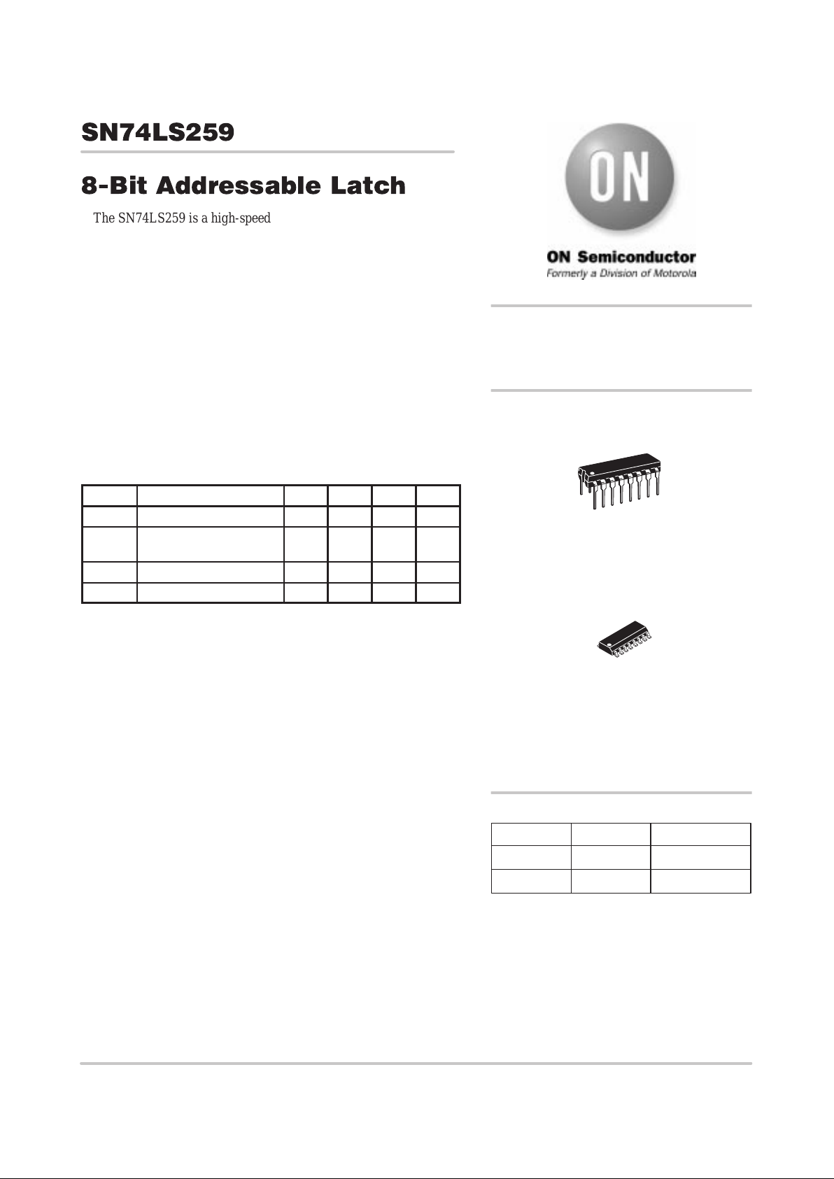
CONNECTION DIAGRAM DIP (TOP VIEW)
Address Inputs
Data Input
Enable (Active LOW) Input
Clear (Active LOW) Input
Parallel Latch Outputs
A
0
, A1, A
2
D
E
C
Q0 – Q
7
0.5 U.L.
0.5 U.L.
1.0 U.L.
0.5 U.L.
10 U.L.
0.25 U.L.
0.25 U.L.
0.5 U.L.
0.25 U.L.
5 U.L.
NOTES:
a) 1 TTL Unit Load (U.L.) = 40 mA HIGH/1.6 mA LOW.
HIGH LOW
(Note a)LOADING
PIN NAMES
14 13 12 11 10 9
123456
7
16 15
8
V
CC
A
o
C E DQ
7
Q
5
Q
6
Q
4
A1A2Q0Q1Q2Q3GND
Page 3
E
C MODE
L
H
L
H
H
H
L
L
Addressable Latch
Memory
Active HIGH Eight-Channel
Demultiplexer
Clear
MODE SELECTION
X = Don’t Care Condition
L = LOW Voltage Level
H = HIGH Voltage Level
Q
N–1
= Previous Output State
SN74LS259
http://onsemi.com
3
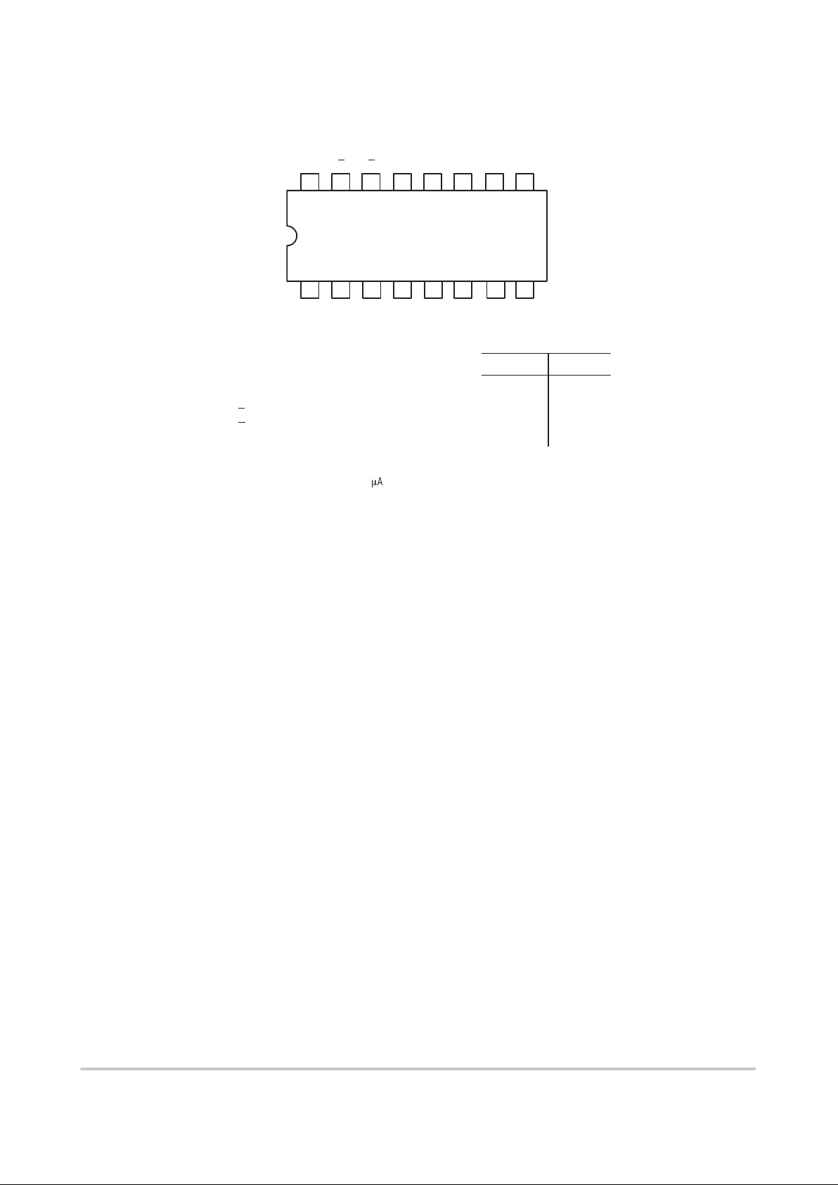
LOGIC DIAGRAM
E DA
0
A1A
2
C
Q
0
Q
1
Q
2
Q
3
Q
4
Q
5
Q
6
Q
7
14 12
67
3
4 5 9 11 1210
13 15
VCC = PIN 16
GND = PIN 8
= PIN NUMBERS
FUNCTIONAL DESCRIPTION
The SN74LS259 has four modes of operation as shown in
the mode selection table. In the addressable latch mode, data
on the Data line (D) is written into the addressed latch.The
addressed latch will follow the data input with all
non-addressed latches remaining in their previous states. In
the memory mode, all latches remain in their previous state
and are unaffected by the Data or Address inputs.
In the one-of-eight decoding or demultiplexing mode, the
addressed output will follow the state of the D input with all
other inputs in the LOW state. In the clear mode all outputs
are LOW and unaffected by the address and data inputs.
When operating the SN74LS259 as an addressable latch,
changing more then one bit of the address could impose a
transient wrong address. Therefore, this should only be done
while in the memory mode.
The truth table below summarizes the operations.
TRUTH TABLE
PRESENT OUTPUT STATES
C E D A0A1A2Q
0
Q
1
Q
2
Q
3
Q4Q
5
Q
6
Q
7
MODE
L H X X X X L L L L L L L L Clear
L LL L L L L L L L L L L L Demultiplex
L LH L L L H LLLLLLL
L LL H L L L LLLLLLL
L LH H L L L HLLLLLL
• •• • •
• •• • •
• •• • •
• •• • •
• •• • •
L LH H H H L LLLLLLH
H H X X X X Q
N–1
Memory
H I I L L L L Q
N–1QN–1QN–1
Addressable
H LH L L L H Q
N–1QN–1
Latch
H LL H L L Q
N–1
LQ
N–1
H LH H L L Q
N–1
HQ
N–1
• •• • •
• •• • •
• •• • •
• •• • •
• •• • •
H LL H H H Q
N–1
Q
N–1
L
H L H H H H Q
N–1
Q
N–1
H
Page 4

SN74LS259
http://onsemi.com
4
DC CHARACTERISTICS OVER OPERATING TEMPERATURE RANGE (unless otherwise specified)
Limits
Symbol Parameter
Min Typ Max
Unit Test Conditions
V
IH
Input HIGH Voltage 2.0 V
Guaranteed Input HIGH Voltage for
All Inputs
V
IL
Input LOW Voltage
0.8
V
Guaranteed Input LOW Voltage for
All Inputs
V
IK
Input Clamp Diode Voltage –0.65 –1.5 V VCC = MIN, IIN = –18 mA
V
OH
Output HIGH Voltage 2.7 3.5 V
VCC = MIN, IOH = MAX, VIN = V
IH
or VIL per Truth Table
p
0.25 0.4 V IOL = 4.0 mA
VCC = VCC MIN,
VOLOutput LOW Voltage
0.35 0.5 V IOL = 8.0 mA
V
IN
=
V
IL
or
V
IH
per Truth Table
p
20 µA VCC = MAX, VIN = 2.7 V
IIHInput HIGH Current
0.1 mA VCC = MAX, VIN = 7.0 V
I
IL
Input LOW Current –0.4 mA VCC = MAX, VIN = 0.4 V
I
OS
Short Circuit Current (Note 1) –20 –100 mA VCC = MAX
I
CC
Power Supply Current 36 mA VCC = MAX
Note 1: Not more than one output should be shorted at a time, nor for more than 1 second.
AC CHARACTERISTICS (T
A
= 25°C, VCC = 5.0 V)
Limits
Symbol Parameter
Min Typ Max
Unit Test Conditions
t
PLH
t
PHL
Turn-Off Delay, Enable to Output
Turn-On Delay, Enable to Output
22
15
35
24
ns
ns
t
PLH
t
PHL
Turn-Off Delay, Data to Output
Turn-On Delay, Data to Output
20
13
32
21
ns
ns
CL = 15 pF
t
PLH
t
PHL
Turn-Off Delay, Address to Output
Turn-On Delay, Address to Output
24
18
38
29
ns
ns
L
t
PHL
Turn-On Delay, Clear to Output 17 27 ns
AC SET-UP REQUIREMENTS (T
A
= 25°C, VCC = 5.0 V)
Limits
Symbol Parameter
Min Typ Max
Unit
t
s
Input Setup Time 20 ns
t
W
Pulse Width, Clear or Enable 15 ns
t
h
Hold Time, Data 5.0 ns
t
h
Hold Time, Address 20 ns
Page 5

SN74LS259
http://onsemi.com
5
t
s
Figure 1. Turn-on and Turn-off Delays, Enable To
Output and Enable Pulse Width
Figure 2. Turn-on and Turn-off Delays,
Data to Output
Figure 3. Turn-on and Turn-off Delays,
Address to Output
NOTES:
1. The Address to Enable Setup Time is the time before the HIGH-to-LOW Enable transition that the Address must be stable so that the correct latch is
addressed and the other latches are not affected.
2. The shaded areas indicate when the inputs are permitted to change for predictable output performance.
OTHER CONDITIONS: C = H, A = STABLE
OTHER CONDITIONS: E
= L, C = H, A = STABLE
OTHER CONDITIONS: E
= L, C = L, D = H
OTHER CONDITIONS: C
= H, A = STABLE
OTHER CONDITIONS: E = H
1.3 V
t
PHL
t
PLH
1.3 V
D
E
Q
1.3 V 1.3 V
1.3 V1.3 V
t
PLH
t
PHL
D
Q
1.3 V
1.3 V
t
PHL
C
Q
1.3 V
1.3 V
1.3 V
1.3 V
1.3 V 1.3 V
A
1
A
1
Q
1
t
PLH
D
E
Q
th(H) th(L)
1.3 V
OTHER CONDITIONS: C
= H
STABLE ADDRESS
A
E
ts(H)
ts(L)
t
PHL
t
w
t
w
Q=D Q=D
AC WAVEFORMS
Figure 4. Setup and Hold Time, Data to Enable
Figure 5. Turn-on Delay, Clear to Output
Figure 6. Setup Time, Address to Enable
(See Notes 1 and 2)
Page 6

SN74LS259
http://onsemi.com
6
P ACKAGE DIMENSIONS
N SUFFIX
PLASTIC PACKAGE
CASE 648–08
ISSUE R
NOTES:
1. DIMENSIONING AND TOLERANCING PER ANSI
Y14.5M, 1982.
2. CONTROLLING DIMENSION: INCH.
3. DIMENSION L TO CENTER OF LEADS WHEN
FORMED PARALLEL.
4. DIMENSION B DOES NOT INCLUDE MOLD FLASH.
5. ROUNDED CORNERS OPTIONAL.
–A–
B
F
C
S
H
G
D
J
L
M
16 PL
SEATING
18
916
K
PLANE
–T–
M
A
M
0.25 (0.010) T
DIM MIN MAX MIN MAX
MILLIMETERSINCHES
A 0.740 0.770 18.80 19.55
B 0.250 0.270 6.35 6.85
C 0.145 0.175 3.69 4.44
D 0.015 0.021 0.39 0.53
F 0.040 0.70 1.02 1.77
G 0.100 BSC 2.54 BSC
H 0.050 BSC 1.27 BSC
J 0.008 0.015 0.21 0.38
K 0.110 0.130 2.80 3.30
L 0.295 0.305 7.50 7.74
M 0 10 0 10
S 0.020 0.040 0.51 1.01
____
Page 7

SN74LS259
http://onsemi.com
7
P ACKAGE DIMENSIONS
D SUFFIX
PLASTIC SOIC PACKAGE
CASE 751B–05
ISSUE J
NOTES:
1. DIMENSIONING AND TOLERANCING PER ANSI
Y14.5M, 1982.
2. CONTROLLING DIMENSION: MILLIMETER.
3. DIMENSIONS A AND B DO NOT INCLUDE
MOLD PROTRUSION.
4. MAXIMUM MOLD PROTRUSION 0.15 (0.006)
PER SIDE.
5. DIMENSION D DOES NOT INCLUDE DAMBAR
PROTRUSION. ALLOWABLE DAMBAR
PROTRUSION SHALL BE 0.127 (0.005) TOTAL
IN EXCESS OF THE D DIMENSION AT
MAXIMUM MATERIAL CONDITION.
18
16 9
SEATING
PLANE
F
J
M
R
X 45
_
G
8 PLP
–B–
–A–
M
0.25 (0.010) B
S
–T–
D
K
C
16 PL
S
B
M
0.25 (0.010) A
S
T
DIM MIN MAX MIN MAX
INCHESMILLIMETERS
A 9.80 10.00 0.386 0.393
B 3.80 4.00 0.150 0.157
C 1.35 1.75 0.054 0.068
D 0.35 0.49 0.014 0.019
F 0.40 1.25 0.016 0.049
G 1.27 BSC 0.050 BSC
J 0.19 0.25 0.008 0.009
K 0.10 0.25 0.004 0.009
M 0 7 0 7
P 5.80 6.20 0.229 0.244
R 0.25 0.50 0.010 0.019
____
Page 8

SN74LS259
http://onsemi.com
8
ON Semiconductor and are trademarks of Semiconductor Components Industries, LLC (SCILLC). SCILLC reserves the right to make changes
without further notice to any products herein. SCILLC makes no warranty , representation or guarantee regarding the suitability of its products for any particular
purpose, nor does SCILLC assume any liability arising out of the application or use of any product or circuit, and specifically disclaims any and all liability ,
including without limitation special, consequential or incidental damages. “Typical” parameters which may be provided in SCILLC data sheets and/or
specifications can and do vary in different applications and actual performance may vary over time. All operating parameters, including “Typicals” must be
validated for each customer application by customer’s technical experts. SCILLC does not convey any license under its patent rights nor the rights of others.
SCILLC products are not designed, intended, or authorized for use as components in systems intended for surgical implant into the body, or other applications
intended to support or sustain life, or for any other application in which the failure of the SCILLC product could create a situation where personal injury or
death may occur. Should Buyer purchase or use SCILLC products for any such unintended or unauthorized application, Buyer shall indemnify and hold
SCILLC and its officers, employees, subsidiaries, affiliates, and distributors harmless against all claims, costs, damages, and expenses, and reasonable
attorney fees arising out of, directly or indirectly , any claim of personal injury or death associated with such unintended or unauthorized use, even if such claim
alleges that SCILLC was negligent regarding the design or manufacture of the part. SCILLC is an Equal Opportunity/Affirmative Action Employer .
PUBLICATION ORDERING INFORMATION
ASIA/PACIFIC: LDC for ON Semiconductor – Asia Support
Phone: 303–675–2121 (Tue–Fri 9:00am to 1:00pm, Hong Kong Time)
T oll Free from Hong Kong 800–4422–3781
Email: ONlit–asia@hibbertco.com
JAPAN: ON Semiconductor, Japan Customer Focus Center
4–32–1 Nishi–Gotanda, Shinagawa–ku, T okyo, Japan 141–8549
Phone: 81–3–5487–8345
Email: r14153@onsemi.com
Fax Response Line: 303–675–2167
800–344–3810 Toll Free USA/Canada
ON Semiconductor Website: http://onsemi.com
For additional information, please contact your local
Sales Representative.
SN74LS259/D
North America Literature Fulfillment:
Literature Distribution Center for ON Semiconductor
P.O. Box 5163, Denver, Colorado 80217 USA
Phone: 303–675–2175 or 800–344–3860 T oll Free USA/Canada
Fax: 303–675–2176 or 800–344–3867 Toll Free USA/Canada
Email: ONlit@hibbertco.com
N. American Technical Support: 800–282–9855 Toll Free USA/Canada
EUROPE: LDC for ON Semiconductor – European Support
German Phone: (+1) 303–308–7140 (M–F 2:30pm to 5:00pm Munich Time)
Email: ONlit–german@hibbertco.com
French Phone: (+1) 303–308–7141 (M–F 2:30pm to 5:00pm Toulouse Time)
Email: ONlit–french@hibbertco.com
English Phone: (+1) 303–308–7142 (M–F 1:30pm to 5:00pm UK Time)
Email: ONlit@hibbertco.com
 Loading...